Durability of the superconducting gap
in Majorana nanowires under orbital effects of a magnetic field
Abstract
We analyze the superconducting gap in semiconductor/superconductor nanowires under orbital effects of a magnetic field in the weak- and strong-hybridization regime using a universal procedure which guarantees the stationarity of the system, i.e., vanishing of the supercurrent induced by a spatially varying vector potential. We perform minimization of the free energy with respect to the vector potential which allows for taking into account the orbital effects even for systems with intrinsically broken spatial symmetry. For the experimentally relevant scenario of a strongly coupled semiconductor/superconductor system, where the wave function of the charge carriers hybridizes between the two materials, we find that the gap closes due to the orbital effects in a sizable magnetic field in correspondence with the recent experiment [S. M. Albrecht, et al., Nature 531, 206 (2016)].
I Introduction
Over the last years Majorana bound states (MBSs), the simplest non-Abelian particles, have attracted the growing interest in the condensed matter physics due to their potential application in fault-tolerant topological quantum computation Kitaev (2003); Alicea (2010). Among theoretical proposals of MBSs creation, including those based on topological insulator-superconductor junctions Fu and Kane (2008), graphene-like systemsBlack-Schaffer (2012); San-Jose et al. (2015); Klinovaja et al. (2012); Zhou et al. (2016) or a chain of magnetic atomsNadj-Perge et al. (2013); Pientka et al. (2013); Pöyhönen et al. (2014); Klinovaja et al. (2013), the most promising one is related to semiconductor nanowires in which topological superconductivity can be induced by the proximity effect in the presence of both the spin-orbit interactionWójcik et al. (2018) and the Zeeman effectOreg et al. (2010); Sau et al. (2010); Lutchyn et al. (2010).
Although the existence of MBSs localized at the ends of a nanowire has been confirmed in experiments Mourik et al. (2012); Deng et al. (2012); Finck et al. (2013); Churchill et al. (2013); Chen et al. (2017); Albrecht et al. (2016); Zhang et al. (2018), a typical experimental setup with a single wire proximitized to a superconductor is insufficient for topological quantum computation. Even an elementary braiding operation requires at least a three terminal junction. Only recently, the extensive progress in synthesis of semiconductor nanowires with a thin Aluminum shell Krogstrup et al. (2015); Gazibegovic et al. (2017) have directed experimental studies towards multiterminal devices Plissard et al. (2013); Fadaly et al. (2017); Gazibegovic et al. (2017) which can be used as prototypes for topological quantum gates Alicea et al. (2011); Heck et al. (2012); Hyart et al. (2013). The pristine interface between semiconductor and superconductor in these heterostructuresKjaergaard et al. (2017), on the one hand guarantees the hard superconducting gap in the nanowireChang et al. (2015), and on the other enables arbitrary alignment of the magnetic field without destroying superconductivityAlbrecht et al. (2016). In practice, the perpendicular orientation of the magnetic field is the most desirable for multiterminal structures as only this alignment allows for inducing the topological phase in all the nanowire branches simultaneously. In this case, the orbital effects of the magnetic field become of high importance since, as shown in Ref. Dmytruk and Klinovaja, 2018, even for the magnetic field aligned with the nanowire axis, they lead to the substantial modification of the topological phase diagram.
The standard way of theoretical treatment of the orbital effects is carried out by the incorporation of the canonical momentum with the appropriate vector potential into the Hamiltonian. However, recent years showed that the numerical adaptation of this method to the Hamiltonian with the particle-hole symmetry, even via the Peierls phase – which makes it robust against discretization errors – leads to ambiguous conclusions differing between subsequent studies.
In the first theoretical analysis of the robustness of MBSs with respect to the magnetic field Lim et al. (2012) the authors stated that even a few degrees of magnetic field titling with respect to the nanowire axis destroys the zero energy modes due to the orbital effects. However, the following paper Osca and Serra (2015) indicated that correct discretization of the Bogoliubov-de Gennes Hamiltonian with the use of the covariant derivative prevents the numerical artifacts which wrongly suggest that MBSs are easily destroyed by the orbital effects. As a result the topological phase can survive sizable vertical field tilting in favor of creation of the zero energy modes. The theoretical treatment of the orbital effects becomes cumbersome in more realistic models of heterostructures that aim at an accurate description of both the semiconducting nanowire and the metallic superconducting shell. Particularly, as argued by Nijholt and Akhmerov in Ref. Nijholt and Akhmerov, 2016, the orbital effects of a magnetic field in the heterostructures with a thin Al shell in the long-junction regime, break spatial and chiral symmetries of the Hamiltonian which leads to the tilting of the band structure and closing of the superconducting gap even for weak magnetic fields.
In the light of the ongoing debate, within this paper we provide careful analysis of the orbital effects on the closing of the superconducting gap. Our study settles the aforementioned ambiguity both for the systems in the weak-coupling regime and in the strong-coupling limit applicable to the recently studied nanowires Krogstrup et al. (2015); Albrecht et al. (2016); Gazibegovic et al. (2017); Reeg et al. (2017). We point out the importance of finding the stationary state of the considered hybrid system – a configuration where the supercurrent induced by the vector potential is zero. Our method is based on the minimization of the free energy with respect to the vector potential which avoids the necessity of a prior choice of the vector potential origin. As we show, such an approach is crucial, since the wrong adaptation of the vector potential into the Hamiltonian, can lead not only to different phase diagrams but also to erroneous conclusions that the topological gap closes in the range of parameters where it is still open. First, the proposed method is demonstrated for the homogeneous nanowires with an uniform energy gap that corresponds to the hybrid structures in the weak-coupling limit. Then, it is used to study the orbital effects in the realistic experimental setup with a thin Al shell where we take into account the strong variance of the material parameters in the heterostructure, providing good agreement with the recent observations Albrecht et al. (2016).
II Model
We consider a two-dimensional (2D) semiconductor nanowire with the Rashba spin-orbit interaction and the superconducting pairing induced by the proximity to a thin superconducting layer. Assuming translational invariance in the -direction, the Hamiltonian of the system in the basis is given by
| (1) | |||||
with,
| (2) |
and where is the spatially dependent effective mass, is the g-factor, is the superconducting gap, is the chemical potential, is the external magnetic field oriented in the -direction, perpendicular to the nanowire plane, and , with are the Pauli matrices acting on spin- and particle-hole degrees of freedom, respectively. In Eq. (1), is the Hamiltonian of the spin-obit interaction
| (3) |
taken in the form that ensures hermiticity for the spatially varying strength of the coupling , where and denotes the anticommutator.
The orbital effects of the magnetic field are included through the canonical momentum, with the vector potential in the Lorentz gauge , where is the offset. Determination of will be discussed in the further part of this article.
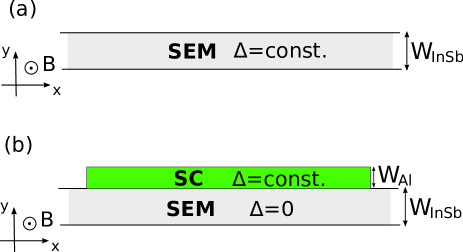
In the following, we first consider a homogeneous nanowire with a uniform superconducting gap inside the wire as presented in Fig. 1(a). It corresponds to the weak-coupling regimeSticlet et al. (2017) with a non-transparent semiconductor/superconductor interface, where the superconductor can be considered as a perturbation providing solely the electron-hole coupling () in the normal region. Then, we proceed to a more realistic model of the Majorana nanowire with a superconducting thin Al shell [see Fig. 1(b)]. In this case all the -dependent quantities in the Hamiltonian (1) have a form of step-like functions with values different for the two materials. For InSb nanowire we assume , , , meVnm while the Al shell is characterized by , , meV, .
Numerical diagonalization of the Hamiltonian (1) for the heterostructure from Fig. 1(b) requires sophisticated discretization, due to the large difference in the effective masses and Fermi energies between semiconductor and superconductor. In order to minimize the numerical errors, the discretization is carried out on a non-uniform grid with two different lattice constants and corresponding to the semiconducting and superconducting components, respectively. Then, the finite differences of the first and second derivatives along the -axis are given by
| (4) | |||
| (5) |
where denotes the average value of the effective mass between the grid points and , respectively.
The numerical calculations are carried out on the rectangular grid with the following parameters: nm, nm, nm and nm unless stated otherwise. The vector potential is introduced into the numerical model through the Peierls substitution . The numerical calculations for the homogeneous system were performed using the Kwant package Groth et al. (2014).
III Results and discussion
III.1 Translation symmetry on a square lattice with a magnetic field
The discrete form of Hamiltonian (1) on the square lattice is given by
| (6) | |||||
where and are the creation and annihilation operators on site , , with being the lattice constant and is the Peierls phase along the -axis in the magnetic field .
Note that the Hamiltonian (6) is no longer invariant under the translation by one unit lattice vector because the corresponding vector potential is not invariant under this discrete translation even though the magnetic field itself might be. It can be easily verified that the translation operators
| (7) | |||||
| (8) |
do not commute with the Hamiltonian (6), . To recover the translational invariance, the new magnetic translational operatorsBernevig and Hughes (2013) have to be constructed with the general form given by
| (9) | |||||
| (10) |
The phases are determined by the requirement which leads to
| (11) |
with
| (12) |
being the magnetic flux per unit cell. For the considered Lorentz gauge the magnetic translational operators are
| (13) | |||||
| (14) |
where .
The operators , commute with the Hamiltonian (6) by construction.
Physically, they correspond to the transformation of the Hamiltonian (wave function) due to the translation by one unit lattice vector along the
and -axis, respectively.
The zero-field form of indicates that the translation along the -axis by an arbitrary vector does not change the Hamiltonian (6). However the translation along the -axis by the vector being integer multiple of the lattice vector with [see Eq. (14)] leads to the acquisition of the phase , opposite for electron and holes, which depends on the position of site on the lattice. In this case, to ensure the gauge-invariance, the Hamiltonian (6) has to be transformed by the unitary operator
| (15) |
The transformation modifies the superconducting pair potential to the form , which guarantees that the supercurrent does not change. Specifically, if this transformation preserves the stationarity of the system. As we will show in the next sections, the requirement of stationarity is indispensable and has to be incorporated in the simulations of the Majorana nanowires that include the orbital effects through the vector potential.
III.2 Homogeneous nanowire
We start from the simple homogeneous nanowire with the uniform energy gap as presented in Fig. 1(a). The induced energy gap is taken to be meV.
III.2.1 Symmetric system
Let us first consider the nanowire localized symmetrically with respect to the -axis and put the offset of the vector potential [see the top-left inset of Fig. 2(a)].
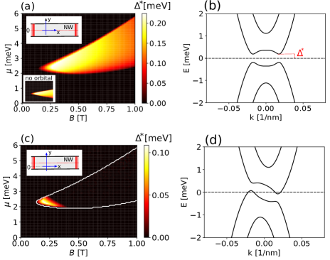
The main quantity under consideration is the topological gap determined from the gapped Dirac cones at in the topological phase as presented in Fig. 2(b). In Fig. 2(a) we plot the map of calculated with the inclusion of the orbital effects as a function of the magnetic field and the chemical potential. The shape of the topological phase contour strongly deviates from the one obtained with sole Zeeman interaction [see the bottom-left inset to Fig. 2(a)] which results from the renormalization of the effective mass, spin-orbit coupling and chemical potential due to the orbital effectsNowak and Wójcik (2018). Dispersion relation for an exemplary set of parameters ensuring the topological phase is presented in Fig. 2(b).
Now, let us transpose the nanowire by the vector with nm keeping the vector potential offset [see the inset in Fig. 2(c)]. Equivalently, we can leave the position of the nanowire unchanged and transform the vector potential changing the offset . In this case, if we do not take care of the appropriate transformation of the Hamiltonian, the particle and hole components acquire opposite phases from the magnetic field as described in III.1. This leads to tilting of the band structure [see Fig. 2(d)] which corresponds to generation of a suppercurrent Chirolli and Guinea (2018a, b), to a significant reduction of the parameter space where the topological gap is nonzero [c.f. Fig. 2(c) with Fig. 2(a)] and the striking conclusion that the magnetic field closes the superconducting gap which makes the creation of Majoranas impossible.
Note that the correct treatment of the Bogoliubov-de Gennes Hamiltonian under the gauge transformation requires an appropriate transformation of the wave function and the superconducting gap . As we checked, in the case of nanowire displacement by the vector when , the numerical results do not depend on the choice of giving the topological phase diagram as presented in Fig. 2(a) even when the system is located as in the inset to Fig. 2 (c). Seemingly, the assurance of the gauge invariance by the aforementioned transformation solves the problem of artificial gap closing. However, in practice the gauge invariance only ensures that the results stay unchanged under the transformation but does not determine the primordial alignment of the system with respect to the vector potential. In other words, we could as well assume that the results from Fig. 2(c)(d) present the physical solution that remains unchanged upon the gauge transformation.
As we present in Sec. III.1, the incorporation of the magnetic field should rather be associated with an additional condition for the vector potential which guarantees stationarity of the system. Physically, it can be achieved by zeroing of the supercurrent due to appropriate choice of the vector potential. Determination of for the considered system comes down to and requires calculation of the eigenvectors. As the presence of the supercurrent corresponds rather to the excited than the ground state, the condition can be alternatively found in a simpler way by minimizing the free energy which for superconducting nanostructures takes the formKosztin et al. (1998)
| (16) | |||||
where are eigenvalues of the Hamiltonian (1), is the Fermi distribution function and is a temperature. is a positive magnetic field exclusion energy due to the screening supercurrent induced by the magnetic field
| (17) |
In practice, to avoid divergence in the expression (16), we calculate it with the respect to the free energy of the corresponding normal state, . Note, that for , reduces to the formula for the condensation energy
| (18) |
where are the eigenvalues of the Hamiltonian (1) in the normal state while can be treated as the energy reference level independent on .
Minimization of with respect to the vector potential is the key point for the inclusion of the orbital effects, which guarantees the stationarity. It can be done by appropriate choice of the vector potential offset 111As presented in sec. III.1 only the translation along the -axis induces the spatially dependent phase and generates the supercurrent. Due to the reflection symmetry with respect to the -axis, for the considered homogeneous nanowire with the chosen Lorentz gauge, the condition requires the vector potential offset being always positioned in the middle of the nanowire. This requirement is not met for the system presented in the inset of Fig. 2(c) and the gap closing in this case is a result of the non-stationarity with . In Fig. 3 we present the condensation energy as a function of the offset calculated for the nanowire shifted by the vector [inset in Fig. 2(c)]. Nanowire boundaries are depicted by the dashed lines.
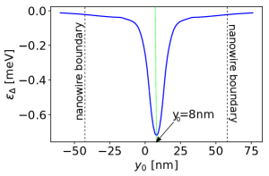
The distinct minimum of the condensation energy, which ensures stationarity of the system (), is localized exactly in the middle of the nanowire as we previously inferred from the symmetry analysis. We also checked, that for the considered homogeneous nanowire, the position of this minimum does not change regardless of the magnetic field and the chemical potential values. The map of the topological gap determined by this method is exactly the same as presented in Fig. 2(a), in which the stationarity is preserved by construction, and does not dependent on the translation vector .
III.2.2 Broken symmetry
For a symmetric system discussed above, even without employing the minimization procedure it was possible to guess the alignment of the vector potential that minimizes the supercurrent. This is however not possible when the spatial symmetry is intrinsically broken by, e.g., potentials in Eq. (1) such the charge distribution in the wire is not know a priori. To demonstrate that let us assume that the system is localized symmetrically about the -axis with the vector potential offset and the symmetry is broken by the applied electric field oriented along the -axis.
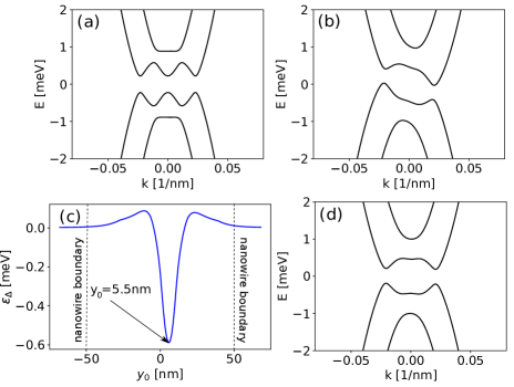
In this case, the sole presence of the transversal electric field without the magnetic orbital effects does not tilt the band structures – are fully symmetric with respect to as presented in Fig. 4(a). The inclusion of the orbital effects breaks the chiral symmetry with leading to the band tilting as presented in Fig. 4(b). Again, not taking care of the stationarity leads to the wrong conclusion that the gap closes already for low magnetic fields [see Fig. 4(b)]. In fact, Fig. 4(b) corresponds rather to the excited state with . The full minimization of the condensation energy [see Fig. 4(c)] clearly indicates that there is a vector potential offset nm that corresponds to the ground state and gives the band structure presented in Fig. 4(d). In contrary to Fig. 4(b) it does not display the gap closing.
III.3 Semiconductor/supercondcutor heterostructure
Finally, we turn our attention to the more realistic model presented in Fig. 1(b), which explicitly treats the thin superconducting Al shell. Before discussing the orbital effects, we start from the brief overview of an appropriate semiconductor/superconductor interface parametrization which ensures the induced gap values as observed in recent experiments on nanowires with an epitaxial Al shell. Very recently the hybridization at the semiconductor/superconductor interface in Majorana devices has been studied by the self-consistent Schrödinger-Poisson approach Mikkelsen et al. (2018); Antipov et al. (2018). It has been pointed out that the quantitative description of the interface requires consideration of the band offset which results from the difference between the electron affinity of the semiconductor and the work function of the metal. As reported in the recent ARPES studiesAntipov et al. (2018), is negative for the epitaxially grown InAs/Al heterostructure supporting the scenario of the band bending which localizes the charge near the semiconductor/superconductor interface. This effect combined with the back-gate electric field substantially strengthens the hybridization between the states at the interface which otherwise is unfavorable due to the large difference between the effective masses and the chemical potentials in both materials.
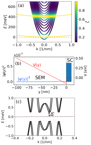
However, even the accumulation of the charge near the semiconductor/superconductor interface does not guarantee the superconducting gap in the semiconductor. In fact, it is possible only if a strongly hybridized band crosses the Fermi level. This can be obtained by an appropriate adjustment of Al electronic states so that the energy of one of them crosses the Fermi level at the vector near the crossing point for the InSb lowest subband. This makes the induced gap sensitive to the Al layer thickness and the value of Mikkelsen et al. (2018). In order to study the orbital effects in an experimentally observed gap regime we assume that the whole heterostructure is attached to the gate from the side of semiconductor, as in the experiment. For simplicity, we do not consider the Hartee potential - the full self-consistent calculations Mikkelsen et al. (2018); Antipov et al. (2018) are time consuming and do not change the main conclusions of our study. Under these assumptions the negative gate voltage generates the triangular-shaped potential [see Fig. 5(b), red dashed line] which together with negative band offset mimics the charge accumulation layer near the interface. In our calculations we take V, eV, and .
In Fig. 5(a) we present the electron band structure of the InSb/Al nanowire obtained by the numerical solution of the Schrödinger equation with the spatially dependent effective mass, chemical potential, spin-orbit constant and -factor. The color of the curves determines how strongly different bands are coupled to the superconductor which is quantified by the amount of the wave function localized in superconductor
| (19) |
The electronic state configuration which ensures strong hybridization at the Fermi level is obtained by the slight modification of the chemical potential to eV from the bulk Al value eVAshcroft and Mermin (1976). This leads to the situation where the substantial part of the wave function is localized in the superconductor - see Fig. 5(b), blue line. Then, as presented in Fig. 5(c), the induced gap meV is close to that assumed for the Al shell.
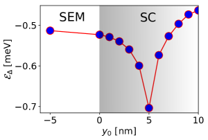
The correct parametrization of the semiconductor/superconductor heterostructure which ensures the strong-coupling regime is crucial for understanding the impact of the orbital effects on the topological gap, compatible with the recent experimental observation. To show that we start from calculations of the condensation energy as a function of the vector potential offset - see Fig. 6. The dependence exhibits the distinct minimum exactly at the middle of superconductor ( nm) Its position is independent on the magnitude of the magnetic field.
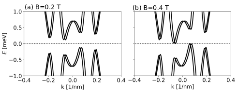
Distinct hybridization of states in the considered strong-coupling regime localizes the wave function in the superconductor near the zero of the vector potential making the induced superconducting gap robust against the orbital effects. The band structures calculated with the inclusion of the orbital effects for different magnetic field magnitudes (see Fig. 7) show that the gap closes for T close to the value reported in the experiment – compare with Fig. 3(d) from Ref. [Albrecht et al., 2016]. Note that, for the case of sole Zeeman interaction the physical restriction for the presence of the induced gap is the critical field of the Al shell above which superconductivity in Al is destroyed. Assuming that the superconducting properties of 10 nm thick Al shell do not strongly deviate from those for the bulk, we can estimate the Pauli paramagnetic limit based on the Clogston-Chandrasekhar formula , where is the Bohr magneton. For the assumed meV, the estimated value T is significantly higher than the one observed experimentally.
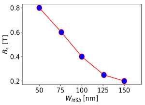
Finally, in Fig. 8 we present the critical field as a function of the nanowire thickness . As expected, the critical field increases for narrower wires. Nevertheless, even for small is much less than the paramagnetic limit indicating the significance of the inclusion of the orbital effects in reliable modeling of topological properties of hybrid nanowires.
IV Summary
We have analyzed the impact of the magnetic orbital effects on the superconducting gap closing in hybrid Majorana nanowires. We have demonstrated that the vanishing of the supercurrent – stationarity – is the necessary condition for a proper description of the semiconductor/superconductor hybrid under the magnetic field. We have proposed that the stationarity can be acquired by minimizing the free energy of the structure with respect to the vector potential. Following that procedure we have studied the superconducting gap in semiconductor/superconductor heterostructures in weak- and strong-coupling regimes. The proposed scheme avoids the need of an a priori choose of the location of the vector potential origin that might lead to erroneous conclusions or even can be simply impossible to determine for systems with intrinsically broken symmetry. Finally, for the realistic heterostructure with a thin Al shell with the account taken to the strong variance of the material parameters, we have found that the critical field is comparable to that reported in the recent measurement for gated nanowiresAlbrecht et al. (2016).
Acknowledgements.
The authors acknowledge helpful discussions with Michał Zegrodnik. P.W. was supported by National Science Centre, Poland (NCN) according to decision 2017/26/D/ST3/00109. M.P.N. was supported by National Science Centre, Poland (NCN) according to decision DEC-2016/23/D/ST3/00394. The calculations were performed on PL-Grid Infrastructure.References
- Kitaev (2003) A. Y. Kitaev, Annals of Physics 303, 2 (2003).
- Alicea (2010) J. Alicea, Phys. Rev. B 81, 125318 (2010).
- Fu and Kane (2008) L. Fu and C. L. Kane, Phys. Rev. Lett. 100, 096407 (2008).
- Black-Schaffer (2012) A. M. Black-Schaffer, Phys. Rev. Lett. 109, 197001 (2012).
- San-Jose et al. (2015) P. San-Jose, J. L. Lado, R. Aguado, F. Guinea, and J. Fernández-Rossier, Phys. Rev. X 5, 041042 (2015).
- Klinovaja et al. (2012) J. Klinovaja, S. Gangadharaiah, and D. Loss, Phys. Rev. Lett. 108, 196804 (2012).
- Zhou et al. (2016) B. T. Zhou, N. F. Q. Yuan, H.-L. Jiang, and K. T. Law, Phys. Rev. B 93, 180501 (2016).
- Nadj-Perge et al. (2013) S. Nadj-Perge, I. K. Drozdov, B. A. Bernevig, and A. Yazdani, Phys. Rev. B 88, 020407 (2013).
- Pientka et al. (2013) F. Pientka, L. I. Glazman, and F. von Oppen, Phys. Rev. B 88, 155420 (2013).
- Pöyhönen et al. (2014) K. Pöyhönen, A. Westström, J. Röntynen, and T. Ojanen, Phys. Rev. B 89, 115109 (2014).
- Klinovaja et al. (2013) J. Klinovaja, P. Stano, A. Yazdani, and D. Loss, Phys. Rev. Lett. 111, 186805 (2013).
- Wójcik et al. (2018) P. Wójcik, A. Bertoni, and G. Goldoni, Phys. Rev. B 97, 165401 (2018).
- Oreg et al. (2010) Y. Oreg, G. Refael, and F. von Oppen, Phys. Rev. Lett. 105, 177002 (2010).
- Sau et al. (2010) J. D. Sau, R. M. Lutchyn, S. Tewari, and S. Das Sarma, Phys. Rev. Lett. 104, 040502 (2010).
- Lutchyn et al. (2010) R. M. Lutchyn, J. D. Sau, and S. Das Sarma, Phys. Rev. Lett. 105, 077001 (2010).
- Mourik et al. (2012) V. Mourik, K. Zuo, S. M. Frolov, S. R. Plissard, E. P. a. M. Bakkers, and L. P. Kouwenhoven, Science 336, 1003 (2012).
- Deng et al. (2012) M. T. Deng, C. L. Yu, G. Y. Huang, M. Larsson, P. Caroff, and H. Q. Xu, Nano Lett. 12, 6414 (2012).
- Finck et al. (2013) A. D. K. Finck, D. J. Van Harlingen, P. K. Mohseni, K. Jung, and X. Li, Phys. Rev. Lett. 110, 126406 (2013).
- Churchill et al. (2013) H. O. H. Churchill, V. Fatemi, K. Grove-Rasmussen, M. T. Deng, P. Caroff, H. Q. Xu, and C. M. Marcus, Phys. Rev. B 87, 241401 (2013).
- Chen et al. (2017) J. Chen, P. Yu, J. Stenger, M. Hocevar, D. Car, S. R. Plissard, E. P. A. M. Bakkers, T. D. Stanescu, and S. M. Frolov, Sci. Adv. 3, e1701476 (2017).
- Albrecht et al. (2016) S. M. Albrecht, A. P. Higginbotham, M. Madsen, F. Kuemmeth, T. S. Jespersen, J. Nygård, P. Krogstrup, and C. M. Marcus, Nature 531, 206 (2016).
- Zhang et al. (2018) H. Zhang, C.-X. Liu, S. Gazibegovic, D. Xu, J. A. Logan, G. Wang, N. van Loo, J. D. S. Bommer, M. W. A. de Moor, D. Car, R. L. M. O. h. Veld, P. J. van Veldhoven, S. Koelling, M. A. Verheijen, M. Pendharkar, D. J. Pennachio, B. Shojaei, J. S. Lee, C. J. Palmstrom, E. P. A. M. Bakkers, S. D. Sarma, and L. P. Kouwenhoven, Nature 556, 74 (2018).
- Krogstrup et al. (2015) P. Krogstrup, N. L. B. Ziino, W. Chang, S. M. Albrecht, M. H. Madsen, E. Johnson, J. Nygård, C. M. Marcus, and T. S. Jespersen, Nat. Mater. 14, 400 (2015).
- Gazibegovic et al. (2017) S. Gazibegovic, D. Car, H. Zhang, S. C. Balk, J. A. Logan, M. W. A. de Moor, M. C. Cassidy, R. Schmits, D. Xu, G. Wang, P. Krogstrup, R. L. M. Op het Veld, K. Zuo, Y. Vos, J. Shen, D. Bouman, B. Shojaei, D. Pennachio, J. S. Lee, P. J. van Veldhoven, S. Koelling, M. A. Verheijen, L. P. Kouwenhoven, C. J. Palmstrøm, and E. P. A. M. Bakkers, Nature 548, 434 (2017).
- Plissard et al. (2013) S. R. Plissard, I. van Weperen, D. Car, M. A. Verheijen, G. W. G. Immink, J. Kammhuber, L. J. Cornelissen, D. B. Szombati, A. Geresdi, S. M. Frolov, L. P. Kouwenhoven, and E. P. A. M. Bakkers, Nat. Nano. 8, 859 (2013).
- Fadaly et al. (2017) E. M. T. Fadaly, H. Zhang, S. Conesa-Boj, D. Car, Ö. Gül, S. R. Plissard, R. L. M. Op het Veld, S. Kölling, L. P. Kouwenhoven, and E. P. A. M. Bakkers, Nano Lett. 17, 6511 (2017).
- Alicea et al. (2011) J. Alicea, Y. Oreg, G. Refael, F. v. Oppen, and M. P. A. Fisher, Nat. Phys. 7, 412 (2011).
- Heck et al. (2012) B. v. Heck, A. R. Akhmerov, F. Hassler, M. Burrello, and C. W. J. Beenakker, New J. Phys. 14, 035019 (2012).
- Hyart et al. (2013) T. Hyart, B. van Heck, I. C. Fulga, M. Burrello, A. R. Akhmerov, and C. W. J. Beenakker, Phys. Rev. B 88, 035121 (2013).
- Kjaergaard et al. (2017) M. Kjaergaard, H. J. Suominen, M. P. Nowak, A. R. Akhmerov, J. Shabani, C. J. Palmstrøm, F. Nichele, and C. M. Marcus, Phys. Rev. Applied 7, 034029 (2017).
- Chang et al. (2015) W. Chang, S. M. Albrecht, T. S. Jespersen, F. Kuemmeth, P. Krogstrup, J. Nygård, and C. M. Marcus, Nat. Nano. 10, 232 (2015).
- Dmytruk and Klinovaja (2018) O. Dmytruk and J. Klinovaja, Phys. Rev. B 97, 155409 (2018).
- Lim et al. (2012) J. S. Lim, L. Serra, R. López, and R. Aguado, Phys. Rev. B 86, 121103 (2012).
- Osca and Serra (2015) J. Osca and L. Serra, Phys. Rev. B 91, 235417 (2015).
- Nijholt and Akhmerov (2016) B. Nijholt and A. R. Akhmerov, Phys. Rev. B 93, 235434 (2016).
- Reeg et al. (2017) C. Reeg, D. Loss, and J. Klinovaja, Phys. Rev. B 96, 125426 (2017).
- Sticlet et al. (2017) D. Sticlet, B. Nijholt, and A. Akhmerov, Phys. Rev. B 95, 115421 (2017).
- Groth et al. (2014) C. W. Groth, M. Wimmer, A. R. Akhmerov, and X. Waintal, New J. Phys. 16, 063065 (2014).
- Bernevig and Hughes (2013) B. A. Bernevig and T. L. Hughes, Topological Insulators and Topological Superconductors (Princeton University Press, Princeton, 2013).
- Nowak and Wójcik (2018) M. P. Nowak and P. Wójcik, Phys. Rev. B 97, 045419 (2018).
- Chirolli and Guinea (2018a) L. Chirolli and F. Guinea, (2018a), arXiv:1806.05969 .
- Chirolli and Guinea (2018b) L. Chirolli and F. Guinea, (2018b), arXiv:1802.09204 .
- Kosztin et al. (1998) I. Kosztin, i. c. v. Kos, M. Stone, and A. J. Leggett, Phys. Rev. B 58, 9365 (1998).
- Note (1) As presented in sec. III.1 only the translation along the -axis induces the spatially dependent phase and generates the supercurrent.
- Mikkelsen et al. (2018) A. E. G. Mikkelsen, P. Kotetes, P. Krogstrup, and K. Flensberg, (2018), arXiv:1801.03439 .
- Antipov et al. (2018) A. E. Antipov, A. Bargerbos, G. W. Winkler, B. Bauer, E. Rossi, and R. M. Lutchyn, (2018), arXiv:1801.02616 .
- Ashcroft and Mermin (1976) N. Ashcroft and N. Mermin, Solid State Physics (Saunders College, Philadephia, 1976).