Aggregation and Electronically-Induced Migration of Oxygen Vacancies in TiO2 Anatase
Abstract
The influence of the electric field and electric current on the behavior of oxygen vacancies (VOs) in TiO2 anatase was investigated with Scanning Tunneling Microscopy (STM). At the anatase (101) surface VOs are not stable; they migrate into the bulk at temperatures above 200 K. Scanning a clean anatase (101) surface at a sample bias greater than +4.3 V results in surface VOs in the scanned area, suggesting that subsurface VOs migrate back to the surface. To test this hypothesis, surface VOs were first created through bombardment with energetic electrons. The sample was then mildly annealed, which caused the VOs to move to the subsurface region, where they formed vacancy clusters. These VO clusters have various, distinct shapes. Scanning VO clusters with a high STM bias reproducibly converts them back into groupings of surface VO, with a configuration that is characteristic for each type of cluster. The dependence of the subsurface-to-surface VO migration on the applied STM bias voltage, tunneling current, and sample temperature was investigated systematically. The results point towards a key role of energetic, ’hot’ electrons in this process. The findings are closely related to the memristive behavior of oxides and oxygen diffusion in solid-oxide membranes.
I Introduction
The influence of electric fields on the behavior of oxygen vacancies (VOs) in metal oxides is of key importance for several applications of these materials. For example, the memristive switching in oxides is a promising approach for data storing.Strukov et al. (2008); Yang et al. (2013); Szot et al. (2014, 2011) While it is clear that field-induced redox reactions and field-induced material migration play a key role,Szot et al. (2011) very little is known about the detailed physical mechanisms and processes occurring at atomic scale.Zheng et al. (2012, 2013) Similar phenomena are also essential in solid-oxide fuel cells, Minh (1993); Steele and Heinzel (2001) where oxygen is transported from the cathode to the anode through the lattice of the oxide electrolyte (typically ZrO2 or CeO2) via migration of oxygen vacancies.
Anatase is a metastable form of the prototypical metal oxide TiO2,Diebold (2003) a material that has been central in oxide research for decades. TiO2 anatase is used in catalysis,Dohnálek et al. (2010) photocatalysis,Linsebigler et al. (1995); Henderson (2011) and dye-sensitized solar cells.Grätzel (2001) Owing to its promising electronical properties, it is also frequently investigated as a memristive materialSzot et al. (2011, 2014) and as a Transparent Conductive Oxide (TCO).Furubayashi et al. (2005)
Recently it was found that the anatase (101) surface does not contain any surface VOs when prepared under ultrahigh vacuum (UHV) conditions by a standard sputter-annealing procedure.He et al. (2009) Surface VOs could be produced non-thermally by bombarding the sample with energetic electrons. These VOs proved unstable and diffused to the subsurface region at temperatures as low as 200 K.Scheiber et al. (2012) In our previous workSetvin et al. (2013) we have created the same atomic-size features by scanning a clean anatase (101) surface at a high sample bias of +5 V. We concluded that these were VOs that most likely originated from electronically induced migration of oxygen vacancies from the subsurface region to the surface.
In this work we investigate this phenomena in detail. The paper is divided into three main parts. In part A we confirm that scanning a clean anatase (101) surface at high positive sample biases creates surface VOs. In part B we verify that the VOs appearing on the surface indeed stem from the subsurface region. To this end we performed the following experiment: First surface VOs were created by electron bombardment of a defect-free surface. Then the sample was annealed above room temperature. This resulted in the migration of VOs to the subsurface region, where they formed VO clusters. Scanning at high bias voltage reproducibly converted these clusters back into a collection of single surface VOs. This is a strong indication that the surface VOs form due to migration of material between the subsurface region and the surface and are not newly created by the STM tip. We also discuss the ramifications of the subsurface VO clustering for surface reactivity. In part C we systematically investigate how the rate of VO creation depends on various parameters (bias voltage US, tunneling current , temperature, and number of scans), and determine the role of the electric field . Based on a quantitative analysis of the experimental results, we conclude that the VO migration occurs close to the field-emission regime in STM, and it depends on only weakly under the experimental conditions used in this work. In part D we discuss the possible physical mechanisms underlying the STM-induced VO migration. We identify the mechanism as one-electron process involving hot electrons. The implications of our results for memristor research are discussed.
II Experimental details
The experiments were performed in a UHV chamber at a base pressure below Pa, equipped with a commercial Omicron LT-STM head. STM measurements were performed at K or K. Electrochemically etched W STM tips were cleaned by Ar+ sputtering and treated on a Au (110) surface to obtain a reproducible, metallic tip condition. An anatase mineral sample was cleavedDulub and Diebold (2010) and cleaned in situ by cycles of Ar+ sputtering and annealing.Setvin et al. (2014a) In a trace analysisSetvin et al. (2013), the highest level of impurity in the sample was determined as 1.1 at. % Nb.
Sample annealing was performed in a manipulator located in an adjacent preparation chamber (base pressure Pa). The temperature was measured with a K-type thermocouple at the heating/annealing stage. We estimate that the quoted temperatures are accurate within K. To create surface VOs, the sample was cooled to 105 K and irradiated with electrons from a thoroughly outgassed, rastered electron gun (500 eV, current density 8 A cm-2).
III Results and Discussion
III.1 STM-induced surface O vacancies
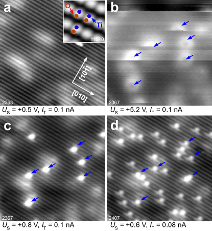
Figure 1 shows the effect of scanning a clean anatase (101) surface with STM at a high positive sample bias. Single VOs appear within the scanned area (and, depending on the tip shape, the surrounding few nm, see ref. Setvin et al., 2013). Figure 1a displays the as-prepared, clean anatase (101) surface; the STM image was taken with standard (low-bias) conditions. Brighter regions correspond to positions of subsurface donors,Ebert (1999) likely extrinsic dopants. Fig. 1b shows the same area, but this time it is scanned at a high sample bias V and a tunneling current nA. Horizontal streaks indicate structural changes that occurred during the high-voltage scan (marked by arrows). The same area is imaged again in Fig. 1c with normal imaging conditions (after two high-bias scans such as the one in (b)). Several new features have appeared in the area; some are marked by arrows. By comparison with -beam induced defectsSetvin et al. (2013); Scheiber et al. (2012) (see also Fig. 2 below) these are identified as surface VOs. When the same area is scanned multiple times at the elevated bias, more oxygen vacancies are created. This is illustrated in Fig. 1d, which shows the same area after 32 high-bias scans at the tunneling parameters of Fig. 1b. For better orientation, the positions of the vacancies created in (b) are marked. It is rare that the VOs move laterally by one position during a high-bias scan. We were not able to remove the VOs with the STM tip, for example by applying a negative .
III.2 Formation and Dissociation of VO clusters
III.2.1 Subsurface vacancy clusters formed by aggregation
The surface VOs shown in the previous section could, in principle, be generated in two different ways: either by desorbing two-coordinated surface O2c atoms (e.g., via electron or field-induced desorption), or by ’pulling’ subsurface VOs to the surface. (More precisely, by pushing surface oxygen atoms deeper into the lattice.) Several previous observations point towards the second possibility. First, the threshold for electron-induced desorption is in the range of tens of eV,Dulub et al. (2007) much higher than what can be achieved in STM. Second, the tip is at a negative potential with respect to the sample, thus it should repel rather than attract the O anions. Third, on TiO2 rutile (110) it was shown that the STM tip can move VOs laterally,Cui et al. (2008) so a vertical motion of VOs is not inconceivable. Nevertheless we designed an experiment to test whether it is indeed the exchange of O between subsurface and surface that gives rise to the effect shown in Fig. 1. We generated surface VOs (now by bombarding with electrons from a conventional electron source) and then annealed the surface. It is known that this results in the migration of the surface vacancies to the subsurface region.Scheiber et al. (2012) We then located the subsurface VOs with STM, and pulled them back to the surface by applying a high sample bias.
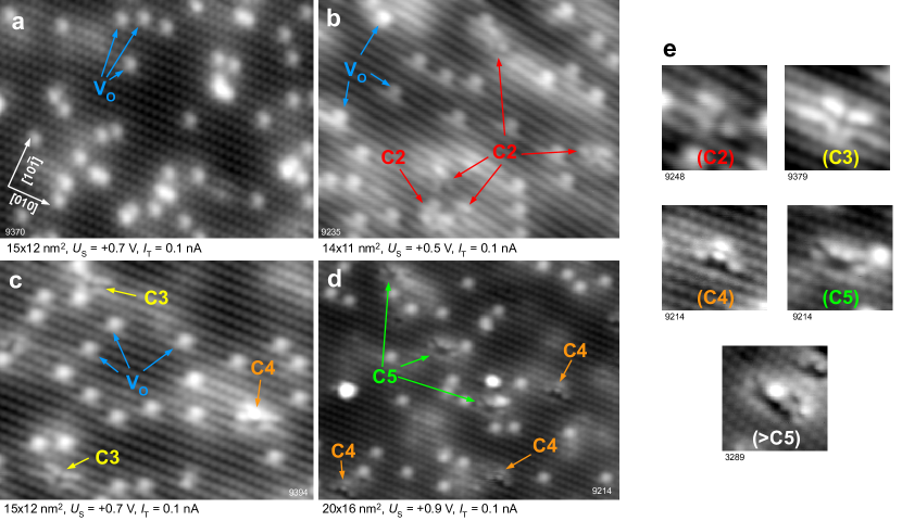
Figure 2a shows the anatase surface after exposing it to the electron beam. Surface VOs are marked. The VO concentration decreases after annealing above 200 K, with no discernible trace in STM images.Scheiber et al. (2012) However, when the annealing temperature exceeds room temperature, new features are observed. Several types formed, with a characteristic and reproducible appearance in STM images. These are marked as C2-C5 in Figs. 2b-e. After annealing to temperatures slightly above 300 K, we observe mostly the features we call C2 (see Fig. 2c) and C3 (Fig. 2b). These two are imaged as distortions of the anatase (101) lattice. They appear as protrusions, slightly shifted in the direction from the maxima of the bright rows. After annealing the surface to higher temperatures (380 to 500 K), larger features appear, see C4 and C5 in Figs. 2b,d and also in ref. Scheiber et al., 2012. An example of one feature larger than C5 is shown at the bottom of Fig. 2e.
The features C2-C5 (as well as larger ones, which are not discussed here) are directly related to the oxygen deficiency in the near-surface region, as judged by the disappearance of surface VOs. We assume that they originate from clustering of the oxygen vacancies that were originally located on the surface, as discussed below. In the nomenclature C2-C5 the number denotes the order in which the clusters form, i.e., C2 forms at the lowest temperatures (320 K) and so forth. The numbers 2-5 are tentatively related to the number of oxygen vacancies in the cluster. The experiments shown below indicate that C2 contains two vacancies, C3 three. It is possible that these ’clusters’ are nucleation centers of more reduced phases of titania, like Ti2O3 or TiO.
We note that the activation energy for hopping of a single surface VO to the first subsurface layer is 0.75 eV according to DFT calculations.Scheiber et al. (2012); Cheng and Selloni (2009a, b) A vacancy can possibly migrate deeper with lower activation barriers (as low as 0.17 eV). The energetically most favorable position for a single vacancy is likely in the first few subsurface layers rather than deep in the bulk; the switching between surface and subsurface sites that we observed for sample temperatures 200–300 K in our previous workScheiber et al. (2012) supports the preferred residence of VOs in near-surface regions. In order to migrate in the direction parallel to the surface, the vacancy has to perform at least one hop with a calculated activation barrier of 1.1 eV.Cheng and Selloni (2009b) The difference in activation energies for vertical vs. lateral diffusion is consistent with our observation that the single surface VOs start to migrate subsurface at temperatures as low as 200 K, but the clusters start to appear above room temperature.
III.2.2 Converting subsurface vacancy clusters into surface vacancies with the STM tip
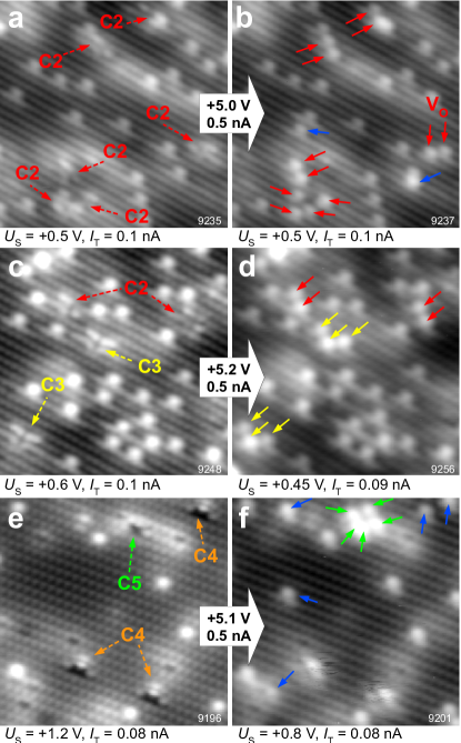
The VO clusters C2-C5 were scanned with a high STM bias. At a positive sample bias voltage of eV the clusters are converted into groupings of single VOs, with each one characteristic for one type of cluster. This is shown in Fig. 3. The panels (a), (c), and (e) on the left show surfaces with various types of VO clusters. These surfaces were prepared as described above, i.e., by bombarding a clean anatase (101) surface with electrons and subsequent annealing to 320, 320, and 380 K, respectively. The STM images in panels (b), (d), and (f) at the right were taken after each area was scanned at the bias voltages and high tunneling currents indicated in the large arrows in Fig. 3.
The high-bias scans cause the disappearance of the surface distortions that are indicative of the VO clusters. The original surface is obtained and surface VOs appear, with a number that is characteristic for each cluster. The cluster C3 is always converted into three VOs that are usually arranged in the triangular pattern shown in Fig. 3d. Cluster C2 is converted into a pair of oxygen vacancies. Larger clusters (C4 and higher) can rarely be converted into single oxygen vacancies (see Fig. 3e, f), even if higher electric fields are applied. Usually the cluster undergoes certain changes and some surface VOs appear, but the original (11) surface could not be restored. Probably the crystal lattice is too distorted for the larger clusters; in addition, interstitial Ti atomsWendt et al. (2008) may already be involved.
The high-bias scans above the clusters were performed both in the constant current and the constant height modes, providing the same result. (We performed this test to ensure that the tip-sample distance is the same above the cluster and the clean surface.) Compared to the sample bias needed to obtain a comparable number of VOs on a clean surface (the experiment in Fig. 1), the bias for converting subsurface VO clusters to surface VOs is only V lower. The similar values indicate that the physical mechanism is the same in both cases: The surface VOs are not generated by desorbing oxygen atoms from the surface, but by transport of material within the sample.
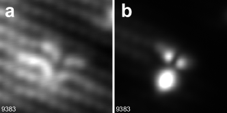
We have investigated the electronic structure of the VO clusters. All the clusters show localized states below the Fermi level, an indication of trapped electrons.Setvin et al. (2014b) As an example, we show empty and filled-states STM images of a C3 cluster in Figs. 4a,b, respectively. The filled-state image of the C3 cluster shows one large and two small spots. The surrounding anatase lattice shows negligible LDOS below , as expected.Setvin et al. (2014b) Scanning tunneling spectroscopy measurements of the C3 cluster (data not shown here) show states at (larger spot) and eV (two smaller spots) below the Fermi level. These states appear shallower than the state for a single surface VO, which is typically eV below EF.Setvin et al. (2014c, b)
III.2.3 Impact of the VO clustering on the materials properties
Our results clearly show that VOs tend to form clusters in the subsurface region. In TiO2 rutile, the extended defects form already at VO concentrations as low as 0.001.Bursill and Smith (1984); Bursill and Blanchin (1984) No such reports exist for anatase so far, but existence of the VO clusters in reduced anatase also seems consistent with photoelectron spectroscopy data, where a considerable Ti2+ signal was detected in a synchrotron-beam-damaged materialJackman et al. (2015) (compared to usual Ti4+ and Ti3+ in rutile).Diebold (2003) The VO clustering must be due to a lower energy as compared to single VOs. As charged vacancies will repel each other, this indicates that VO clusters are neutral or carry only a single negative charge per cluster. We note that the vacancy charge state can be possibly influenced by other defects nearby, thus the clustering may be affected by impurities in the material for example.
The presence of the VO clusters needs to be considered in the various applications of this materials. For example, single subsurface VOs are frequently considered in calculations of chemical reactions. In previous studies it was proposed that subsurface VOs can migrate back to the surface upon adsorption of certain species, and directly participate in chemical reactions.Setvin et al. (2013); Li and Gao (2014) It was predicted theoretically that adsorption of an O2 molecule above a subsurface VO should result in the migration of the VO towards the surface and in a bridging interstitial dimer (O2)O.Setvin et al. (2013) However, in the same work it was shown experimentally that this reaction occurs rarely. The number of (O2)O features obtained in this way was only on the order of 0.1 to 1% ML. A similar reaction was theoretically predicted for H2O adsorption. Reaction of a H2O molecule with a subsurface VO should result in two bridging hydroxyl groups.Li and Gao (2014) This reaction has never been observed experimentally, however. Instead it is known that water adsorbs molecularly on the anatase (101) surface.Aschauer et al. (2010) The VO clustering observed here may explain why it is rare that the vacancies enter the chemical reactions. Theoretical works so far only investigated the configuration of a single subsurface oxygen vacancy. Our results indicate that more favorable configurations exist, where several VOs are bunched together in a cluster. Breaking such cluster is therefore energetically more costly than moving a single VO from the subsurface region to the surface. The single subsurface VOs are probably a rare species on the anatase (101) surface compared to oxygen vacancies on the rutile (110) surface.
The observed behavior of the VO clusters is also closely related to the memristor research. We have shown that annealing of a reduced anatase surface leads to the clustering of the VOs. On the other hand, the clusters can be disassembled back into single VOs under influence of applied electric field and tunneling current. It is known that the formation of extended defects and reduced Magneli phasesBursill and Smith (1984); Bursill and Blanchin (1984) and their transformation back into the stoichiometric oxide is a key process in the memristive switching. We have observed the initial step of the VO aggregation and decomposition. In the following section, we perform a statistical analysis of the experimental data and characterize physical mechanisms responsible for the VO migration.
III.3 Physical mechanisms of STM-induced VO migration
III.3.1 Dependence of VO formation on STM parameters
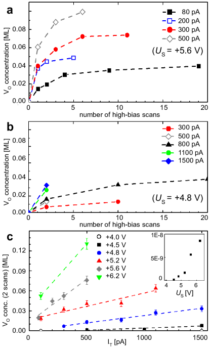
For simplicity, we focus on single vacancies, i.e., we start each experiment with a clean surface and conduct experiments as the one laid out in Figure 1. We investigate how the sample bias, tunneling current, and number of scans affect the concentration of VOs that form during such high-bias scans. Our main findings are summarized in Fig. 5. In Fig. 5a, we chose a fixed V for the high-bias scans and investigated the concentration of VOs in dependence of the number of the scans. This procedure was repeated for different tunneling currents. A new surface area was used for each value of . During all experiments shown in Fig. 5 the size of the scan area and the total scan time were kept constant at nm2 and s, respectively. A similar data set with a lower V is shown in Fig. 5b.
The results in Fig. 5a show that the VO density approaches a saturation value that depends on the tunneling parameters. We then investigated the rate of VO generation in the zero VO concentration limit, the initial slope of the curves in Fig. 5a. This is depicted in Fig. 5c for different combinations of and . Plotted is the VO concentration obtained after the first two high-bias scans. Within the range of currents investigated here (80 to 1500 pA) this initial rate is roughly proportional to the tunneling current, a clear indication for a single-electron process. The proportionality is less precise in the data sets measured at higher , as the curves approach the saturation value faster and the assumption of the zero VO concentration is not perfectly fulfilled.
To estimate the dependence on the sample bias, the curves in Fig. 5c were fitted by a linear function . The slope is plotted in the inset of Fig. 5c. Here the -axis is given in units of cross section , using the known value of the scanned area and scan time per frame . No vacancies are generated below a threshold bias of V. From the available data we judge that the dependence follows a polynomial behavior above the threshold, likely quadratic or cubic.
The data shown in Fig. 5 have been measured at temperature of 78 K. A similar experiment was performed at K, with a comparable result. This suggests that the VO migration is not activated thermally.
III.3.2 Electric field
The results in Fig. 5 clearly show that a threshold (or perhaps a threshold electric field ) is necessary so that subsurface VOs move to the surface (or, conversely, surface O are pushed into the lattice) during STM scans. The initial rate of surface/subsurface O exchange is rougly proportional to , suggesting that a one-electron process is involved. The rate shows a polynomial dependence on above the threshold of +4.3 V. The tip-induced vacancy migration is self-limiting, and the final VO concentration after many scans also depends on and (Fig. 5c).
In tip-induced processes, the tunneling current , bias voltage , and electrical field inside the sampleSelcuk and Selloni (2014) can all play a role. It is not trivial to disentangle how depends on the tunneling parameters. The tip-sample distance depends on and , and only part of the field penetrates into the semiconductor due to screening. This ’tip-induced band-bending (TIBB)’, in turn, can depend on the presence of surface VOs.
To determine the electric field at the conditions where VOs appear, we performed local spectroscopy measurements. To avoid high tunneling currents, spectroscopy with a closed feedback loop was used. The measurement time for the curves was set as low as possible (100 ms/curve), in order to avoid additional creation of vacancies during the measurements. The data shown are averages of 10 curves measured at different positions. Figure 6a shows the result in terms of the absolute tip-sample separation . We calibrated by ’touching the surface’ (see refs. Jelinek et al., 2008; Setvin et al., 2014b). For V and nA, we estimate that nm, all other values can be derived by measuring and spectra.
In Fig. 6b we converted the measured curves into the external electric field acting between the tip and the surface. The electric field is approximately . A more precise expression
| (1) |
takes into account the local contact potential difference between the tip and the sample, . We use a value of +0.6 V, assuming work functions of 5.1 and 4.5 eV for the anatase surface and the tip, respectively.Xiang et al. (2007); Scanlon et al. (2013); Loth (2008) The factor 0.94 in eqn. (1) is a correction for the TIBB – we estimate that of the applied bias penetrates into the sample. This value was obtained with Feenstra’s Poisson equation solver,Feenstra et al. (2005) for various combinations of relevant input parameters. This relatively low level of TIBB results from the high dielectric constant of anatase (),Selcuk and Selloni (2014); Gonzalez et al. (1997) and high sample doping. (Our sample is Nb dopedSetvin et al. (2013) with to cm-3.)
In order to know whether the surface VOs influence the electric fields acting in the system, we performed measurements in a region where such VOs had been created with the STM tip, see dashed lines in Fig. 6. The spectra were taken at least two lattice constants away from VOs (concentration of 7%). There is a small, but reproducible difference in measurements and estimates between clean and defective areas.
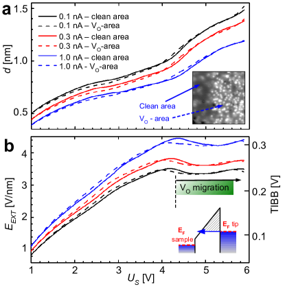
The curves in Fig. 6b show a plateau above V. This is explained by the tunneling scheme in the inset of Fig. 6b. When the applied approaches the sample work function, the tunneling barrier (hatched area) only depends on the electric field between the tip and the sample. The field emission regime is almost reached. Interestingly, the onset of this plateau coincides with the threshold for tip-induced vacancy creation, V. The electric field is roughly constant in the whole regime of tip-induced vacancy migration ( V; inset in Fig. 6b). On the other hand, the rate of VO migration increases dramatically with in this range. This clearly shows that the voltage dependence is not related to the field. The values of the electric field in the regime of vacancy migration, 3.3–4.5 V/nm (depending on , see Fig. 6b) correspond to a TIBB of 0.25–0.30 V inside the sample.
This allows direct comparison of our experimental conditions to the density functional theory calculations performed by Selcuk et. al.Selcuk and Selloni (2014) The calculations show that an electric field inside the anatase sample affects the energetics of surface subsurface VOs. The surface VO should become 0.2 eV more favorable at electric fields comparable to our experimental conditions. On the other hand, the field does not reduce the energy barrier for VO migration from the subsurface to surface, which remains 0.5 to 0.9 eV. In the following we will argue that hot electrons that are injected from the STM tip into the sample help overcoming this activation barrier.
III.3.3 Quantitative analysis
We have measured data sets similar to the one in Fig. 5a for five different values of . All data shown below were obtained with a single STM tip. Here we analyze these results to determine how the VO concentration scales with the physical quantities , , , and the time .
The data are plotted in Fig. 7. The points measured for each single value of collapse to a single line if we scale the axes in a suitable way. Our initial data analysis has shown that the VO migration is initiated by a single-electron process. Thus an appropriate scale for the -axis is the time multiplied by the current density . This product is the electron dose per unit area applied during a scan or a sequence of scans; it does not depend on how the tunneling current is distributed under the tip. The -axis shows the VO concentration , divided by the electric field . We found that this scaling is necessary to collapse the values for different on one line. The value of for each data point was determined from Fig. 6b. The scaling used in Fig. 7a efficiently separates the effects of and , as all the data sets obtained for single values of follow lines on a linear-log scale. The parameter was varied to maximize the R-factors of linear fits in all data, resulting in V/nm. We note that scaling the -axis by is a simple approximation of any -dependence, as the range of used in our experiments is very small (Fig. 6b). Scaling by or provides a very similar result.
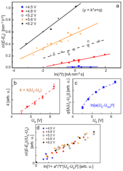
The data points in Fig. 7a are fitted by linear curves
| (2) |
where and now only depend on . By fitting and by suitable functions (shown in Fig. 7b,c) and inserting these functions into Eq. 2, we arrive at an analytical expression
| (3) |
Here V and and are constants. (For details of the fitting, including the meaning of parameters displayed in Fig. 7c and the origin of the ”+1” in Eq. 3, see the Appendix.) Using Eq. 3 we can scale all experimental data points into a single linear dependence, see Fig. 7d. We note that Eq. 3 is the solution of equation
| (4) |
where is the vacancy flow towards the surface. In the following we analyse Eq.4 to gain insight into the physics of the STM-induced vacancy migration.
III.4 Discussion of possible physical mechanisms
The equation has a form of d/d. Here is a rate, which is exponentially ”damped” by VOs already present at the surface. is proportional to the current density . The term has the largest influence on the cross-section of the process. The STM bias voltage is the maximum energy of the electrons injected into the sample. A minimum energy () is needed, and the rate strongly increases with the electron energy above this threshold. In other words, ”hot electrons” are needed. One possibility is that the electrons must be injected into a specific electron state in the conduction band to initiate the VO migration. The importance of injecting the electrons into -orbitals has previously been proposed for tip-induced migration of hydrogen atoms absorbed in bulk palladium.Blanco-Rey et al. (2012); Sykes et al. (2005); Mitsui et al. (2007) While such a process must remain speculative at this point, we note that the experimental value of V matches the region where the -character of the conduction band changes to -like according to theoretical calculations of the anatase band structure.Landmann et al. (2012); Setvin et al. (2014b)
The damping term indicates that the efficiency of the electronic excitations decreases with growing surface VO concentration. The influence of the VOs already present on the surface can be suppressed by applying a higher electric field and a higher . The first term could be due to surface VOs screening the field penetrating into the sample. This decreases the TIBB, which is a necessary component of the VO migration process. The dependence on may be related to scattering the hot electrons at the surface VOs. Each VO provides two localized electrons with a state 1 eV deep in the band gap. The electrons injected from the tip can possibly excite the VO-electrons to the conduction band, resulting in a significant energy loss of the primary electron. The term in the exponential would be then related to the cross-section of this electron-electron scattering process.
A brief summary of the role of and is following: determines the energy of electrons injected into the material. This in turn determines to which particular energy band in the conduction band they are injected and the energy available for single-electron processes. The tunneling current influences the process in two ways. First, it determines the rate of electronic excitations (rate is a linear function of ). Second, is linked to the electric field acting in the system (see Fig. 6). We note that for constant-current conditions, the electric field does not change significantly with in the regime used for inducing the VO migration.
Our finding that hot electrons play a role in the VO migration is in agreement with memristor research. In ref. Szot et al., 2014 it is argued that simple Joule heating may not be the only mechanism involved in defect migration within the crystal. Hot electrons may be directly scattered at defects in the oxide lattice, providing energy for material transport. Our experiments also show that the electric field layout inside the sample plays a certain role. The field helps to revert the energy balance in the material, providing a direction for the vacancy flow. The value of the electric field varies only slightly under our experimental conditions, therefore the field-dependence could not be exactly characterized and was only approximated by a linear function in the equations.
IV Conclusions
We have shown that scanning the anatase (101) surface at high positive sample bias results in the appearance of surface VOs in the scanned area. We attribute this effect to a migration of VOs from the subsurface region to the surface. The process is self-limiting: presence of VOs on the surface prevents further subsurface-to-surface VO migration. Analysis of the experimental data indicates that the electric field penetrating into the sample is an important factor for reverting the energy balance between the surface and subsurface VOs. The hot electrons injected from the tip provide the activation energy necessary for the VO migration through the lattice.
It was further shown that VOs can easily form subsurface clusters upon annealing. We identified VO clusters that contain two to five vacancies. Likely this is the initial step in the formation of extended defects and reduced TiO2-x phases. Subsurface aggregates of VOs can be converted back into single surface VOs by applying a suitable electric field. This process closely resembles memristive switching: Two distinct states exist, one that is reached upon thermal annealing and another one by applying a high electric field. The memristive behavior of oxides have been investigated for more than 50 years, yet there is essentially no knowledge about processes occurring at atomic scale. Our results could provide a significant step forward to identifying the underlying physical mechanisms.
Acknowledgements.
This work was supported by the ERC Advanced Research Grant ‘OxideSurfaces’, and by the Austrian Science Fund (FWF) under project number F45.References
- Strukov et al. (2008) D. B. Strukov, G. S. Snider, D. R. Stewart, and R. S. Williams, Nature 453, 8 (2008).
- Yang et al. (2013) J. J. Yang, D. B. Strukov, and D. R. Stewart, Nat. Nanotechnology 8, 13 (2013).
- Szot et al. (2014) K. Szot, G. Bihlmayer, and W. Speier, Solid State Physics 65, 353 (2014).
- Szot et al. (2011) K. Szot, M. Rogala, W. Speier, Z. Klusek, A. Beshmen, and R. Waser, Nanotechnology 22, 254001 (2011).
- Zheng et al. (2012) H. Zheng, J. Kröger, and R. Berndt, Phys. Rev. Lett. 108, 076801 (2012).
- Zheng et al. (2013) H. Zheng, A. Weismann, and R. Berndt, Phys. Rev. Lett. 110, 226101 (2013).
- Minh (1993) N. Q. Minh, J. Am. Chem. Soc. 76, 563 (1993).
- Steele and Heinzel (2001) B. C. H. Steele and A. Heinzel, Nature 414, 345 (2001).
- Diebold (2003) U. Diebold, Surf. Sci. Rep. 48, 53 (2003).
- Dohnálek et al. (2010) Z. Dohnálek, I. Liubinetsky, and R. Rousseau, Prog. Surf. Sci. 85, 161 (2010).
- Linsebigler et al. (1995) A. Linsebigler, G. Lu, and J. Yates, Chem. Rev. 95, 735 (1995).
- Henderson (2011) M. A. Henderson, Surf. Sci. Rep. 66, 185 (2011).
- Grätzel (2001) M. Grätzel, Nature 414, 338 (2001).
- Furubayashi et al. (2005) Y. Furubayashi, T. Hitosugi, Y. Yamamoto, K. Inaba, G. Inoda, Y. Hirose, T. Shimada, and T. Hasegawa, Appl. Phys. Lett. 86, 252101 (2005).
- He et al. (2009) Y. He, O. Dulub, H. Z. Cheng, A. Selloni, and U. Diebold, Phys. Rev. Lett. 102, 106105 (2009).
- Scheiber et al. (2012) P. Scheiber, M. Fidler, O. Dulub, M. Schmid, U. Diebold, W. Hou, U. Aschauer, and A. Selloni, Phys. Rev. Lett. 109, 136103 (2012).
- Setvin et al. (2013) M. Setvin, U. Aschauer, P. Scheiber, Y.-F. Li, et al., Science 341, 988 (2013).
- Dulub and Diebold (2010) O. Dulub and U. Diebold, J. Phys. Cond. Matt. 22, 084014 (2010).
- Setvin et al. (2014a) M. Setvin, B. Daniel, V. Mansfeldova, L. Kavan, P. Scheiber, M. Fidler, M. Schmid, and U. Diebold, Surf. Sci. 626, 61 (2014a).
- Ebert (1999) P. Ebert, Surf. Sci. Rep. 33, 121 (1999).
- Dulub et al. (2007) O. Dulub, M. Batzil, S. Solovev, E. Loginova, A. Alchagirov, T. E. Madey, and U. Diebold, Science 317, 1052 (2007).
- Cui et al. (2008) X. Cui, B. Wang, Z. Wang, T. Huang, Y. Zhao, J. Yang, and J. G. Hou, J. Chem. Phys. 129, 044703 (2008).
- Cheng and Selloni (2009a) H. Cheng and A. Selloni, Phys. Rev. B 79, 092101 (2009a).
- Cheng and Selloni (2009b) H. Cheng and A. Selloni, J. Chem. Phys. 131, 054703 (2009b).
- Wendt et al. (2008) S. Wendt, P. T. Sprunger, E. Lira, et al., Science 320, 1755 (2008).
- Setvin et al. (2014b) M. Setvin, C. Franchini, X. Hao, M. Schmid, A. Janotti, M. Kaltak, C. V. de Walle, G. Kresse, and U. Diebold, Phys. Rev. Lett. 113, 086402 (2014b).
- Setvin et al. (2014c) M. Setvin, X. Hao, B. Daniel, J. Pavelec, Z. Novotny, G. S. Parkinson, M. Schmid, G. Kresse, C. Franchini, and U. Diebold, Angew. Chem. Intl. Ed. 53, 4714 (2014c).
- Bursill and Smith (1984) L. A. Bursill and D. J. Smith, Nature 309, 319 (1984).
- Bursill and Blanchin (1984) L. A. Bursill and M. G. Blanchin, J. Sol. Stat. Chem. 51, 321 (1984).
- Jackman et al. (2015) M. Jackman, A. G. Thomas, P. Deak, K. L. Syres, et al., arXiv:1406.3385 (2015).
- Li and Gao (2014) Y. Li and Y. Gao, Phys. Rev. Lett. 112, 206101 (2014).
- Aschauer et al. (2010) U. Aschauer, Y. He, H. Cheng, S.-C. Li, U. Diebold, and A. Selloni, J. Phys. Chem. C 114, 1278 (2010).
- Selcuk and Selloni (2014) S. Selcuk and A. Selloni, J. Chem. Phys. 141, 084705 (2014).
- Jelinek et al. (2008) P. Jelinek, M. Svec, P. Pou, R. Perez, and V. Chab, Phys. Rev. Lett. 101, 176101 (2008).
- Xiang et al. (2007) G. Xiang, R. Shao, T. C. Droubay, A. G. Joly, K. M. Beck, S. A. Chambers, and W. P. Hess, Adv. Func. Mater. 17, 2133 (2007).
- Scanlon et al. (2013) D. O. Scanlon, C. W. Dunnil, J. Buckeridge, S. A. Shevlin, et al., Nat. Materials 12, 798 (2013).
- Loth (2008) S. Loth, Atomic Scale Images of Acceptors in III-V Semiconductors, PhD. thesis (Universität Göttingen, 2008).
- Feenstra et al. (2005) R. M. Feenstra, S. Gaan, G. Meyer, and K. H. Rieder, Phys. Rev. B 71, 125316 (2005).
- Gonzalez et al. (1997) R. J. Gonzalez, R. Zallen, and H. Berger, Phys. Rev. B 55, 7014 (1997).
- Blanco-Rey et al. (2012) M. Blanco-Rey, M. Alducin, J. I. Juaristi, and P. L. de Andres, Phys. Rev. Lett. 108, 115902 (2012).
- Sykes et al. (2005) E. C. H. Sykes, L. C. Fernandez-Torres, S. U. Nanayakkara, B. A. Mantooth, R. M. Nevin, and P. S. Weiss, Proc. Natl. Acad. Sci. USA 102, 17907 (2005).
- Mitsui et al. (2007) T. Mitsui, E. Fomin, D. F. Ogletree, M. Salmeron, A. U. Nilekar, and M. Mavrikakis, Angew. Chem. Int. Ed. 46, 5757 (2007).
- Landmann et al. (2012) M. Landmann, E. Rauls, and W. G. Schmidt, J. Phys. Cond. Matt. 24, 195503 (2012).
*
Appendix A Fitting details
Fitting the data points in Fig. 7a by provides dependencies and displayed in Figs. 7b,c, respectively. The appears linear, , with V and V-2nm-1. One can rewrite Eq. 2 as
| (5) |
We can fit the quantity as a function of (see Fig. 7c). A suitable function is logarithmic, we use an ansatz of . Based on the initial analysis in Fig. 5 we guess an close to 2, and similar to . Fitting the plot in Fig. 7c indeed provides , V, and A-1s-1V-α. We will further consider and . The relation for can be expressed as
| (6) |
The disadvantage of this equation is its divergence at . By taking the derivative of Eq. 6, we obtain the differential equation Eq. 4. By solving this equation, we obtain an integration constant: ”+1” in the logarithm, see Eq. 3. This ensures the initial condition at . With the integration constant known, we repeated all the fitting in Fig. 7a. It turns out that the impact on all values obtained from the fitting is very small, as the ”+1” term in the logarithm is negligible for most data points. The only fitting constant that is affected significantly is . The new value of A-1s-1V-α was used in Fig. 7d.
We note that the fitting presented in this paper leads to the final equation 4 in the form d/d. We have tried other ways of fitting the data, especially those leading to the Langmuir-type behavior d/d. The experimental data do not fit such a behavior well.