Machine Learning Peeling and Loss Modelling of Time-Domain Reflectometry
Abstract
A fundamental pursuit of microwave metrology is the determination of the characteristic impedance profile of microwave systems. Among other methods, this can be practically achieved by means of time-domain reflectometry (TDR) that measures the reflections from a device due to an applied stimulus. Conventional TDR allows for the measurement of systems comprising a single impedance. However, real systems typically feature impedance variations that obscure the determination of all impedances subsequent to the first one. This problem has been studied previously and is generally known as scattering inversion or, in the context of microwave metrology, time-domain “peeling”. In this article, we demonstrate the implementation of a space-time efficient peeling algorithm that corrects for the effect of prior impedance mismatch in a nonuniform lossless transmission line, regardless of the nature of the stimulus. We generalize TDR measurement analysis by introducing two tools: A stochastic machine learning clustering tool and an arbitrary lossy transmission line modeling tool. The former mitigates many of the imperfections typically plaguing TDR measurements (except for dispersion) and allows for an efficient processing of large datasets; the latter allows for a complete transmission line characterization including both conductor and dielectric loss. 222This work has been submitted to the IEEE for possible publication. Copyright may be transferred without notice, after which this version may no longer be accessible.
Index Terms:
Time-domain reflectometry, scattering, peeling, iterative procedure, data post-processing, machine learning, K-means, lossy transmission lineI Introduction
Time-domain reflectometry (TDR) is a microwave measurement technique based on the response of a device under test (DUT) to a step stimulus incident upon it [1, 2, 3]. This response is used to determine the characteristic impedance of the DUT along its electrical length. Theoretically, the incident stimulus is assumed to have zero rise time. In reality, however, this is impossible due to the finite bandwidth of all practical systems. As a consequence, the response exhibits a nonzero rise time that, if not accounted for, limits the measurement resolution. Another typical analysis assumption is that the DUT contains only a single reflection plane, whereas, in reality, many reflection planes exist. Independent of the nature of the stimulus, multiple reflection planes induce multiple re-reflections due to the stimulus interacting with previously encountered reflection planes. In addition, another often neglected phenomenon of real structures is dissipation. This results in the deterioration of the response due to signal loss. The degree to which information regarding a lossy DUT can be recovered is of active interest in the field of microwave metrology.
A variety of solutions have been proposed to ameliorate some of the TDR imperfections in the lossless case. For example, in the study of [4], the process of inverse scattering, known as “peeling”, has been introduced to microwave time-domain measurements; similarly, the works of [5] and [6] have proposed a peeling algorithm in the frequency domain. An extension of the time-domain peeling algorithm has been attempted in the study of [7], where a partial solution to the problem of loss is provided. Finally, TDR utilizing arbitrary stimuli has been investigated in the work of [8].
In this article, we study the conditions of applicability of the lossless time-domain peeling algorithm in [4] and revisit the algorithm in the context of a machine learning technique known as K-means clustering or, for brevity, K-means [9]. We show that K-means can be used to post-process a TDR response through data clustering, thus simplifying the data structure and expediting peeling. The use of K-means in TDR has special utility when considering detailed measurements that comprise a large number of data points. Such a level of detail requires more memory to store the data and more time to post-process it. K-means effectively equates comparable measured samples at the benefit of reduced memory consumption and peeling computation time. Additionally, K-means allows us to study systems with finite rise time response as well as to efficiently account for fluctuations due to imperfections in the stimulus, DUT, or measurement device.
Furthermore, we address lossy systems by extending the time-domain fitting technique in [7], which accounts for series resistance only. We introduce a generalized frequency-domain fitting technique, which, instead, accounts for both series resistance and shunt conductance. Provided an appropriate model for the relevant circuit parameters of interest, our fitting technique makes it possible to determine both resistive and reactive circuit components as arbitrary functions of frequency.
The article is organized as follows: In Section II, we outline in detail many of the common issues plaguing conventional TDR measurements and data post-processing; in Section III, we propose a set of solutions and assess their efficacy by analyzing an actual measurement; finally, in Section IV, we discuss a possible combination of the tools introduced here and outline future developments. Additionally, the article features an appendix, Appendix A, where we review the basic theory of TDR peeling and loss fitting.
A complete library including the codes used to implement our K-means TDR peeling algorithm and circuit parameter fitting is available as an open-source software package in [10]; the codes are written in the Julia language [11]. The basic principles of the peeling part of the K-means TDR peeling algorithm are in Appendix A.
II Commonly-Encountered Issues
A metrologist must consider the operations that are applied by the measurement device to the acquired data. In fact, the typical quantity reported by TDR instruments when measuring a DUT is an improper reflection coefficient-like quantity [12]
| (1) |
where “” indicates referring the impedance back to the source impedance (with ), is the th sample of the reflected voltage [13], and is the amplitude of the step stimulus. For a DUT containing only a single reflection plane encountered at section , (1) corresponds to the reflection coefficient for (denoted as ). However, in the presence of multiple reflection planes, (1) has no physical meaning and the reflection coefficients of the DUT can only be obtained by using a peeling algorithm.
When considering a DUT characterized by small variations of its reflection coefficients, a peeling algorithm may not offer a significant improvement over (1). In fact, in the limit of a DUT with a constant reflection coefficient such an algorithm is not even required. Therefore, it is reasonable to question the degree of variation requiring the use of a peeling algorithm in order to appreciably improve measurement results. An answer to this question can be found by analyzing the reflected voltage as a function of repeated reflections.
Consider, for example, the reflected voltage measured at time . Assuming a lossless devices, the reflected voltage can be determined as
| (2) | |||||
where is the th sample of the incident voltage; each () is the reflection (transmission) coefficient between the th and th medium, with (lossless assumption). The naïve approach taken to calculate from the measured data is to use (1), resulting in the improper coefficient
| (3) |
This result is only reasonable if all transmission coefficients are very close to one. Equation (2) can be rewritten in terms of only reflection coefficients (since the device is lossless) as
| (4) | |||||
By further assuming that (the case for a step stimulus), we obtain
| (5) | |||||
A general expression for the improper does not exist due to the lack of a closed form solution for all paths (see Appendix A for a definition of path) that contribute to the reflected voltage at discrete time . However, the general expression for the proper , i.e., the reflection coefficient relating the source characteristic impedance to the th characteristic impedance section of the DUT, can be determined according to (13) in Appendix A as
| (6) |
where
| (7) |
and
| (8) |
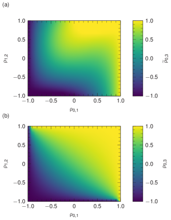
with . A comparison between (5) and (6) for is shown in Fig. 1 (a) and (b).
Other common issues are due to nonidealities present in the stimulus, DUT, or measurement device that obscure information regarding the impedance profile of the DUT. Such nonidealities include unstable stimuli, environmental sensitivity and fabrication imprecisions of the DUT, or noisy measurement devices. For example, the exact nature of a stimulus can affect the efficacy of peeling algorithms significantly. In fact, the nonzero rise time of all real stimuli, if not accounted for, may result in measurements that can be misread as having had resulted from a lossy DUT. Additionally, the application of peeling to a response from such a stimulus can artificially underreport the reflection coefficients of the DUT.
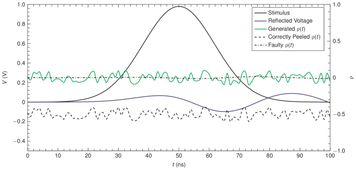
Fig. 2 shows a simulated TDR measurement of a DUT with known reflection coefficients using a Gaussian stimulus. If the peeling algorithm is applied assuming an ideal step stimulus instead of the Gaussian stimulus, the resulting calculated reflection coefficients are drastically different than the known ones. This simulation is performed using the inverse of this work’s peeling algorithm implementation.
Another consideration that must be made when post-processing the reflected voltage are the small voltage variations that appear in measurements of all constant impedance transmission lines. These variations can be the end result of many phenomena: Source noise; dispersion; manufacturing or setup imperfections (e.g., trace-width variation, cable deformation, etc.); measurement noise. It is often desired by the metrologist to ignore electrically brief small variations in the reflected voltage in order to intentionally neglect artifacts irrelevant to the study of the DUT. We address some of the issues outlined here in Subsection III-A.
Finally, one last issue is the characterization of devices comprising homogeneous segments of transmission line whose circuit parameters are arbitrarily complicated functions of frequency. One simple case is that of a DUT characterized by dielectric loss. In fact, almost all practical microwave interconnects (microstrip, coplanar waveguide, etc.) exhibit conductance between the signal and ground lines, resulting in dielectric loss. The study of this loss is performed, for example, when characterizing a new substrate. As another example, the development of superconducting microwave devices often requires consideration of electric properties such as kinetic inductance, which is a nonlinear function of frequency [14]. In this case, a more general solution than the one described in Subsection A-B is required (see Subsection III-B).
III Results
In this section, we introduce a K-means TDR peeling technique (see Subsection III-A) and an extended loss fitting technique (see Subsection III-B).
III-A K-Means Peeling
The rapidly increasing sampling rates of microwave instruments, such as TDR systems, will result in ever-increasing numbers of measured samples. The state-of-the-art analog-to-digital converters achieve sampling rates of approximately using either conventional electronics [15] or superconducting electronics [16]. These sampling rates are at least ten times larger than those used at present in standard microwave electronics and would correspond to more than a ten-fold increase in the spatial resolution of a DUT when employed, e.g., in TDR systems. Moreover, using frequency-domain measurements to perform TDR indirectly, e.g., with a vector network analyzer, it is possible to obtain an almost arbitrarily large number of samples. The measurement of a DUT using these systems will thus require compression for feasible post-processing of the data. Notably, compression provides further advantage when applying state-of-the-art peeling algorithms with runtime .
An immediate application of compression is found when considering small time-domain fluctuations present in TDR measurements. In fact, it can be difficult to determine whether these fluctuations are due to the stimulus, changes in characteristic impedance, or noise in the measurement device. For a reflected voltage containing many such fluctuations it can be desirable to approximate them with a particular value, resulting in a compression of the measured data. This is a remarkable example where removing unnecessary data points using a heuristic (e.g., machine learning) approach leads to more useful data, which are not “contaminated” by unwanted or unknown phenomena.
Another potential application of TDR data compression is to neglect nonzero rise time present in the reflected voltage. Performing this operation in the context of a nearly lossless DUT or a non-step stimulus serves to reject nonidealities without losing important measurement information.
Compressing TDR measurements in such a way as to address the aforementioned problems can be accomplished efficiently using a machine learning tool called K-means [9]. In the field of machine learning, it is often needed to associate a set of vectors () with a set of vectors about which the vectors are clustered. Such clustering algorithms are applied heavily in the subfield of unsupervised machine learning.
In this work, we apply the K-means peeling algorithm to the TDR measurement of a DUT in order to improve data post-processing. First, the reflected voltage data is fed to a K-means implementation that clusters the measured voltages into sections of any one of values. Determining a value for is a heuristic process that requires some attention from the metrologist. We recommend selecting a value of determining segment lengths that are the smallest the metrologist would consider. Then, the peeling algorithm is applied to the clustered voltage samples, realizing a K-means TDR peeling algorithm. This algorithm is best applied to any DUT that comprises distinct homogeneous segments of potentially unequal length. The application of K-means to the data disregards any nonzero rise time associated with the stimulus, or response, or both and also any small variations that may exist in the measured reflected voltage due to noise anywhere in the measurement system.
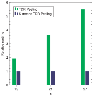
Fig. 3 demonstrates the speed advantage gained by using the K-means TDR peeling algorithm compared to simple TDR peeling. Compared in the figure is the runtime of K-means TDR peeling given three simulated measurements, with , , and points, respectively. The runtime of K-means TDR peeling is significantly lower than that of only TDR peeling. This is due to the downsampling of the response. The speed-up only depends on the difference between the number of sections before and after clustering. Although K-means clustering algorithms typically have a time complexity of , it has been recently shown that this threshold can be lowered to [17]. Therefore, in K-means TDR peeling the complexity of the peeling part of the algorithm dominates that of K-means clustering.

To gauge the efficacy of the K-means TDR peeling algorithm in a practical context, a microstrip stepped impedance DUT is designed and fabricated on a printed circuit board (PCB). A scaled layout of the DUT (as well as its material properties) is supplied in Fig. 4. The design of this PCB is based on two criteria:
-
1.
Include many consecutive large changes in impedance;
-
2.
ensure the round-trip delay of the smallest segment is much greater than the sampling rate of the measurement device.
The first criterion, in particular, is important to ensure that multiple re-reflections significantly impact the measured voltage. In fact, small impedance variations would result in re-reflections that are too small to be detected with the TDR system used in our experiments, which is from Teledyne LeCroy, model WaveExpert 100H. 333The TDR oscilloscope features an electrical sampling module with bandwidth and a TDR step generator, model ST-20. The generated signal is a voltage square wave characterized by a nominal pulse rise time of , amplitude of , pulse width of , and pulse repetition rate of . The input and output impedance of this TDR system, the impedance of Port 1 and Port 2 in Fig. 4, is . 444A single measurement comprising a single terminating impedance (in this case, the load of Port 2) is sufficient to characterize the DUT. Given the nature of peeling, measurements using other load impedances would not affect the determination of the impedance profile of the DUT. Thus, the PCB impedance values are chosen such as to vary significantly relative to . Given the ease of manufacturing microstrip impedances between and on a standard copper-clad FR-4 substrate, the design shown in Fig. 4 is chosen. 555The microstrip PCB is fabricated using a circuit board plotter from LPKF Laser & Electronics AG, model LPKF ProtoMat S.
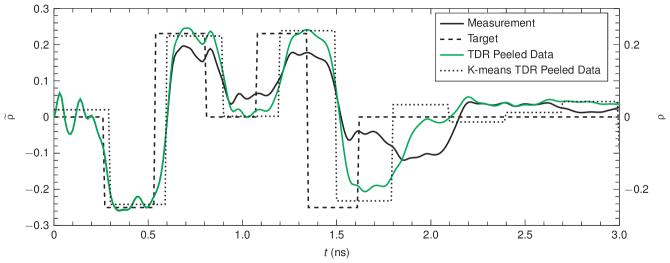
Our PCB design has the advantage of being symmetric, so that TDR measurements can be performed from both ports of the DUT for comparison. Additionally, the impedance varies significantly between different impedance steps exacerbating the effect of multiple re-reflections interfering at the source. The time-domain measurement of the microwave PCB and the result of clustering the data for a number of different cluster sizes are shown in Fig. 5.
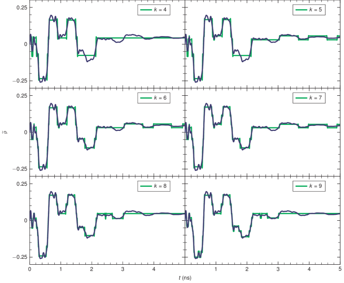
Using the measurement values as reported by the TDR system, we can immediately identify the pitfalls of using the improper reflection coefficient of (1). The reflection coefficient (occurring at ) is reported to be , as designed. The second value, however, is reported to be less than , which is significantly smaller than the designed reflection coefficient of . It is in such situations that K-means TDR peeling harbors most potential. The efficaciousness of K-means clustering combined with peeling is shown in Fig. 6, which demonstrates that the determination of all reflection planes is improved compared to the improper (naïve) case. Note that the disagreement between the theoretical result (target) and the K-means peeled measurement can be attributed to the dispersion and loss of the DUT, which are not accounted for.
While K-means peeling seemingly involves ad hoc manipulation of measured data, this can serve to the benefit of the metrologist. Measured data unavoidably contains artifacts unrelated to the properties of the DUT, which originate from both the source and measurement instruments. The effect of these artifacts on the measured data is usually assumed to be negligibly small. However, due to the nonlinear nature of the peeling algorithm, a reflected voltage signal containing small artifacts can radically affect the peeled measurement. Applying K-means clustering prior to peeling has the potential to average the effect of zero-mean noise introduced by both the source and meter. This potentially improves the data used as input to a peeling algorithm. Comparing the results of peeling both with and without the application of K-means clustering provides a mechanism for determining the degree of error introduced in the measurement as a result of a nonideal source and meter.
III-B Extended Loss Fitting
Dissipation in electrical systems typically arises from radiative, conductor, and dielectric loss, with radiative loss being a negligible effect in many practical scenarios. All these effects depend on frequency, as in the case of conductor losses due to the skin effect [13]. The reactive components of a DUT, i.e., inductance and capacitance, also depend on frequency, as in the case of the kinetic inductance in superconductors [14]. Given appropriate theoretical frequency-domain models of each circuit parameter, it is possible to determine their contribution to the response. We find these parameters by extending the fitting technique described in [7]. While in that study the fitting method has been performed in the time domain and accommodates only a subset of all circuit parameters (see Section II), our method is performed in the frequency domain and accommodates all circuit parameters which, additionally, can be arbitrary functions of frequency.
The characteristic impedance of a transmission line is given by (16) in Appendix A. Thus, the knowledge of , , , and makes it possible to determine the time-domain response of the DUT. However, even if a detailed knowledge of the geometrical and material properties of the DUT is provided, it is impractical to construct a complete circuit-parameter model. Typical approximations to all circuit parameters are given by (14) and (15) in Appendix A, as well as
| (9) |
where is the per-unit-length capacitance and the imaginary part of the relative electric permittivity of the DUT substrate. These assumptions result in the five parameter frequency-domain model of the characteristic impedance
| (10) |
that applies to a wide variety of lossy transmission lines.
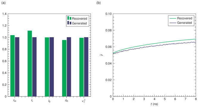
Determining the parameters in (10) requires fitting them to a sequence of measured data points in the frequency domain. In order to assess the efficacy of this fitting scheme we:
-
1.
Simulate the time-domain response of a DUT to a step stimulus using the inverse of our peeling algorithm;
-
2.
introduce noise associated with both the stimulus and measurement device using a pseudorandom number generator;
-
3.
perform a discrete Fourier transform of the time-domain response to determine the frequency-domain response of the DUT;
-
4.
fit the frequency-domain response obtained in 3) using a nonlinear least-squares fitting routine based on the Levenberg-Marquardt algorithm.
This procedure serves to recover all five parameters in (10). The time-domain response of the recovered DUT and the recovered parameters are shown in Fig. 7.
As another example of the broad applicability of this fitting scheme, we consider the case of a superconductor at a temperature below its critical temperature , . Using the surface impedance of a superconductor in lieu of (14) and (15), we can write the characteristic impedance model of a homogeneous section of superconducting transmission line segment as [14]
| (11) |
where is the magnetic constant, the London penetration depth of the superconductor, the conductivity of the normal state conductor, and the length of the superconducting transmission line segment. A similar fitting scheme as the one enumerated above can be used to find all five frequency-dependent circuit parameters in (11).
IV Conclusion
In this article, we introduce a TDR peeling algorithm based on the K-means clustering method that provides a significant improvement over known alternatives such as in [4, 5, 6]. We show examples where traditional peeling algorithms fail and present a practical case study to benchmark the K-means TDR peeling and demonstrate its superiority over traditional peeling. While we apply this machine learning method to the case of TDR measurements, other related techniques can be used in a wider variety of measurement post-processing tasks. This is particularly important in the era of big data, where large datasets allow for more precise and accurate measurements of devices at the cost of increased memory requirements and post-processing runtime.
In addition, we present a method to perform an extended characterization of devices using a fitting scheme that makes it possible to account for a DUT described by a parametrized frequency-domain model. This fitting scheme can be used in conjunction with the K-means TDR peeling algorithm in order to assess devices comprising multiple homogeneous segments, as proposed in [7]. We show frequency-domain models for both normal conductors and superconductors.
It is worth noting that, in some instances, it may be necessary to account for dispersion when applying the K-means TDR peeling algorithm. An example of this can be seen in Fig. 6, where the algorithm is applied to a microstrip transmission line. We will address this issue in future work since it affects a variety of microwave systems. Additionally, a TDR peeling algorithm involving measurements with aperiodic samples would provide large benefit when combined with K-means clustering and should be the focus of further investigations. Finally, a generalized peeling technique accommodating lossy devices that does not require nonlinear fitting is desired and merits further attention.
Acknowledgment
This research was undertaken thanks in part to funding from the Canada First Research Excellence Fund (CFREF), as well as the Discovery and Research Tools and Instruments Grant Programs of the Natural Sciences and Engineering Research Council of Canada (NSERC) and the Ministry of Research and Innovation (MRI) of Ontario. We acknowledge our fruitful discussions with Eric Bogatin, Thomas G. McConkey, and A. Hamed Majedi; JRR acknowledges his fruitful discussions with Behrooz Semnani.
Appendix A A Primer on Peeling and Loss Fitting
In this section, we review the state-of-the-art on TDR peeling algorithms (see Subsection A-A) and loss fitting techniques (see Subsection A-B).
A-A Peeling
A TDR measurement of a DUT with multiple reflection planes requires post-processing in order to accurately characterize the DUT. The stimulus used in these measurements is a travelling voltage wave, which is scattered within the DUT due to the presence of reflection planes. Each scattered component arrives at the measurement plane at delayed times, in accordance with its scattering history, and there interferes with other scattered components. Thus, there exists a one-to-one correspondence between a path through the DUT and a reflected voltage component. The path weight, which is the reflected voltage amplitude for a path, is determined by the stimulus as well as the value of each encountered reflection coefficient. All of these components combine to form the total measured voltage response, which is the signal used to assess the DUT. This process can be inverted using peeling algorithms, which are designed to determine the reflection coefficients of the DUT from the measured reflected voltage [4, 5, 6].
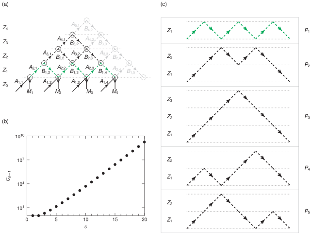
Fig. 8 (a) shows a schematic representation of a DUT characterized by multiple reflection planes, where the scattered voltage can take different paths through the DUT. Each path carries information regarding the reflection planes that it encounters when travelling from the source to the measurement device. These paths are characterized by forward- and backward-oriented segments labeled as and , respectively, with .
In general, time-domain reflectometers attempt to sample the reflected voltage at a periodic time interval , which determines an implicit discretization of the DUT into a set of sections whose electrical properties can be determined by the measured voltage (see [3] for detailed TDR measurement information). Each measured sample must, a priori, be assumed to be associated with one reflection plane, even if it is of zero value. Suppose there are voltage samples of an -section DUT whose length is such that (). In this case, it can be shown that the number of paths associated with the planes is the Catalan number for [18],
| (12) |
Fig. 8 (b) illustrates the strong functional dependence of (12) on the number of planes. Note that for , is greater than the estimated number of particles in the universe. Storing the information regarding all of the paths is impractical considering the scaling behavior of (12). Notably, this is unnecessary since the paths can be constructed using only information from reflection planes. For example, Fig. 8 (c) indicates that paths each of segments can be computed with only reflection coefficients. Thus, the solution is not to solve for all the weights of all paths, but to recursively compute the values of the reflection coefficients by computing the values of each segment once. This is the essence of state-of-the-art time-domain peeling algorithms.
In order to determine the reflected voltage contribution from each path it is necessary to consider the weight of each segment used to construct it. These weights are determined by the nature of the impedance profile. Each impedance variation introduces a possible reflection or transmission event, or both, forming a node in Fig. 8 (a). A numerical implementation of the recursive time-domain peeling algorithm in the lossless case is in [10]. This algorithm generates an array corresponding to and operates in runtime , with the number of measured reflected voltage samples.
An efficient approach to peeling utilizes two facts:
-
1.
The th acquired sample is the first sample with information regarding the th reflection plane;
-
2.
only one path involves the th reflection plane at the th time step.
Having had determined the proper reflection coefficients of the DUT by peeling, the impedance profile of the DUT can be determined by
| (13) |
A-B Loss Fitting
The most general microwave model of a DUT involves four per-unit-length quantities that are each a function of frequency (in units of hertz) [13]: The series resistance ; the series inductance ; the shunt capacitance ; the shunt conductance . Prior work has established a time-domain fitting method to determine these quantities, with the exception, however, of [7]. This partial fitting is performed under the assumptions:
-
1.
(14) where is the dc series resistance per unit length, a skin effect-related resistance per unit length and per root hertz, , and “sgn” the signum function (cf. [19]);
-
2.
(15) where and are a constant inductance and capacitance per unit length, respectively;
-
3.
.
The characteristic impedance of any section of a DUT can be expressed as
| (16) |
Considering a DUT satisfying the three aforementioned assumptions, (16) can be simplified to
| (17) |
Assuming to be small relative to , this expression can be expanded in a Maclaurin series to first order yielding
| (18) |
Multiplying (18) by the Fourier transform of a step function and then performing an inverse Fourier transform results in a time-domain function that can be fitted using a suitable optimization routine. This procedure makes it possible to obtain the four constant parameters , and . In order to implement the fitting procedure, it is necessary to measure a sequence of time-domain reflected voltage values obtained from a DUT with constant circuit parameters over its electrical length, i.e., a DUT that is spatially homogeneous with respect to these parameters. When combining this procedure with the peeling algorithm, it is possible to characterize a nonhomogeneous DUT that contains a set of homogeneous sections.
References
- [1] J. Strickland, Time-domain Reflectometry Measurements, ser. Measurement concepts. Tektronix, 1970. [Online]. Available: https://books.google.ca/books?id=CBNQPQAACAAJ
- [2] G. Bryant, Principles of Microwave Measurements (IEEE Electrical Measurement). The Institution of Engineering and Technology, 1993.
- [3] Agilent Technologies, Inc., Time Domain Reflectometry Theory, ser. Application Note 1304-2, May 2013.
- [4] J. M. Jong and V. K. Tripathi, “Time-domain characterization of interconnect discontinuities in high-speed circuits,” IEEE Transactions on Components, Hybrids, and Manufacturing Technology, vol. 15, no. 4, pp. 497–504, Aug 1992.
- [5] J. Izydorczyk, “Microwave time domain reflectometry,” Electronics Letters, vol. 41, no. 15, pp. 848–849, 2005.
- [6] ——, “Comments on ”time-domain reflectometry using arbitrary incident waveforms”,” IEEE Transactions on Microwave Theory and Techniques, vol. 51, no. 4, pp. 1296–1298, April 2003.
- [7] P. Liu, J. Zhang, and J. Fang, “Accurate characterization of lossy interconnects from tdr waveforms,” in 2013 IEEE 22nd Conference on Electrical Performance of Electronic Packaging and Systems, Oct 2013, pp. 187–190.
- [8] T.-W. Pan, C.-W. Hsue, and J.-F. Huang, “Time-domain reflectometry using arbitrary incident waveforms,” IEEE Transactions on Microwave Theory and Techniques, vol. 50, no. 11, pp. 2558–2563, Nov 2002.
- [9] J. Wu, Advances in K-means Clustering: A Data Mining Thinking (Springer Theses: Recognizing Outstanding Ph.D. Research). Springer, 2012.
- [10] J. Rinehart, “TimeDomainReflectometryPeeling.jl: Functioning Version,” May 2017. [Online]. Available: https://zenodo.org/record/1040412
- [11] J. Bezanson, S. Karpinski, V. B. Shah, and A. Edelman, “Julia: A fast dynamic language for technical computing,” 2012.
- [12] LeCroy, Wave Expert 100H Equivalent Time Sampling Oscilloscope System: Operator’s Manual.
- [13] R. E. Collin, Foundations for Microwave Engineering - 2nd edition. Wiley-IEEE Press, 2001.
- [14] [Online]. Available: https://www.wmi.badw.de/teaching/Lecturenotes/AS/AS_Chapter8.pdf
- [15] H. Huang, J. Heilmeyer, M. Grozing, and M. Berroth, “An 8-bit 100-GS/s distributed DAC in 28-nm CMOS,” in 2014 IEEE Radio Frequency Integrated Circuits Symposium. IEEE, jun 2014. [Online]. Available: https://doi.org/10.1109%2Frfic.2014.6851659
- [16] A. Inamdar, S. Rylov, A. Talalaevskii, A. Sahu, S. Sarwana, D. E. Kirichenko, I. V. Vernik, T. V. Filippov, and D. Gupta, “Progress in design of improved high dynamic range analog-to-digital converters,” IEEE Transactions on Applied Superconductivity, vol. 19, no. 3, pp. 670–675, June 2009.
- [17] M. K. Pakhira, “A linear time-complexity k-means algorithm using cluster shifting,” in 2014 International Conference on Computational Intelligence and Communication Networks, Nov 2014, pp. 1047–1051.
- [18] T. Kim and D. S. Kim, “A new approach to catalan numbers using differential equations,” 2016.
- [19] H. Johnson and M. Graham, High Speed Digital Design: A Handbook of Black Magic. Prentice Hall, 1993.
![[Uncaptioned image]](/html/1804.04756/assets/jr_rinehart_tdr.jpg) |
John R. Rinehart received the Bachelor of Science degree in electrical engineering summa cum laude in from Gonzaga University, Spokane, USA. From to , he was with LHC2 Inc., where he helped develop antenna receiver architectures. In the summer of , he worked alongside researchers from the Martinis Group at the University of California, Santa Barbara, USA, on the implementation of a packaging technique for superconducting quantum bits (qubits). Since , he is enrolled in the quantum information graduate program at the Institute for Quantum Computing (IQC) at the University of Waterloo (UW), Waterloo, Canada, as a PhD candidate in physics. In Waterloo, Rinehart is part of a team developing both classical and quantum technologies for quantum computing with superconducting devices. John R. Rinehart co-authored peer-reviewed articles and is a student member of the IEEE. |
![[Uncaptioned image]](/html/1804.04756/assets/jh_bejanin_tdr.jpg) |
Jérémy H. Béjanin received the Bachelor of Science degree in physics in from McGill University, Montreal, Canada. Since then, he is enrolled in the quantum information graduate program at the IQC at UW, Waterloo, Canada, as a PhD candidate in physics. In Waterloo, he is part of a team developing both classical and quantum technologies for quantum computing with superconducting devices. His current research focuses are on superconducting qubits and resonators, optimal control theory, as well as quantum many-body physical models. Béjanin co-authored peer-reviewed articles. |
![[Uncaptioned image]](/html/1804.04756/assets/tc_fraser_tdr.jpg) |
Thomas C. Fraser received the Bachelor of Science degree in Honours Co-operative Mathematical Physics (Astrophysics Specialization) in from the UW, Canada. In , he was awarded the UW Mike Lazaridis Scholarship in Theoretical Physics at the Perimeter Institute (PI) for Theoretical Physics, Canada. In , he received the Governor General’s Academic Medal (Silver Medal) for academic excellence. Since , he has been pursuing a master’s degree as a student of the Perimeter Scholars International (PSI) program at PI with interest in quantum information. In particular, Fraser’s current research is concerned with systematically identifying the resources provided by entangled quantum states through the perspective of causal inference. |
![[Uncaptioned image]](/html/1804.04756/assets/m_mariantoni_tdr.jpg) |
Matteo Mariantoni (MScEng’04) received a doctorate degree in physics (Dr. Rer. Nat.) summa cum laude in from the Technical University of Munich, Germany. In Munich, he performed experiments on propagating quantum microwave fields and worked on scalable quantum computing architectures. In , he was awarded the Elings Prize Fellowship in Science of the California NanoSystems Institute at the University of California, Santa Barbara, USA. During his postdoctoral research in Santa Barbara, Mariantoni’s implementation of a quantum memory and processor on a single chip using a “quantum von Neumann architecture” was ranked as one of the top breakthroughs for by Physics World. In December , he moved to the IQC at the UW, Waterloo, Canada, as an Assistant Professor in the Department of Physics and Astronomy, where he leads a team developing both classical and quantum technologies for quantum computing with superconducting devices. He was awarded an Alfred P. Sloan Research Fellowship in as well as the Ontario Early Researcher Award and the Kavli Fellowship from the National Academy of Sciences in . Mariantoni co-authored peer-reviewed articles totaling more than citations and authored one book. |