Synthesizing Coulombic superconductivity in van der Waals bilayers
Abstract
Synthesizing a polarizable environment surrounding a low-dimensional metal to generate superconductivity is a simple theoretical idea that still awaits a convincing experimental realization. The challenging requirements are satisfied in a metallic bilayer when the ratio between the Fermi velocities is small and both metals have a similar, low carrier density. In this case, the slower electron gas acts as a retarded polarizable medium (a “dielectric” environment) for the faster metal. Here we show that this concept is naturally optimized for the case of an atomically thin bilayer consisting of a Dirac semimetal (e.g. graphene) placed in atomic-scale proximity to a doped semiconducting transition metal dichalcogenide (e.g. WSe2). The superconducting transition temperature that arises from the dynamically screened Coulomb repulsion is computed using the linearized Eliashberg equation. In the case of graphene on WSe2, we find that can exceed 100 mK, and it increases further when the Dirac valley degeneracy is reduced. Thus, we argue that suspended van der Waals bilayers are in a unique position to realize experimentally this long anticipated theoretical concept.
I Introduction
In 1964 Little Little (1964) argued that superconductivity can be synthesized in low-dimensional conductors by placing them in proximity to a highly polarizable medium which converts the Coulomb repulsion into an effective attraction. The idea attracted much attention due to the prediction of exceptionally high transition temperatures and was developed in many directions Ginzburg (1964); Allender et al. (1973); Bardeen (1978); Merlin (1990); Gutfreund and Little (1996); Malozovsky and Fan (1996); Cotleţ et al. (2016); Kavokin and Lagoudakis (2016); Hamo et al. (2016). Nonetheless, there are no convincing experimental realizations of this elegant theoretical idea; superconductivity has not been synthesized using a polar medium thus far.
Naively, attractive Coulomb interactions are a promising route to high-temperature superconductivity. However, converting the full strength of Coulomb repulsion into attraction poses major challenges, even theoretically. The first is that high density metals screen the Coulomb interaction quite effectively, thus suppressing the coupling strength. Moreover, to be effective, the separation between the metal and the polarizable medium must be smaller than the interparticle distance. Thus, the most promising approach for the conductor is to use semimetals or doped semiconductors in which particle densities are low enough such that the interparticle distance can be greater than a few interionic distances. The second challenge is that a stable dielectric medium has a positive static permittivity. Therefore, instantaneous attraction can only be obtained due to the quantum effects of “over-screening”, as demonstrated by Ref. Hamo et al. (2016). In the absence of such effects, the attraction must be generated dynamically, á la Anderson and Morel Morel and Anderson (1962), which also reduces its bare strength.
These two challenges are anti-cooperative. On the one hand, low-density metals entail a small Fermi energy, reducing the upper limit to the superconducting gap. On the other hand, dynamical generation of attraction is efficient only when the Fermi energy is much greater than the characteristic frequencies in the dielectric medium, which are comparable in practice. For example, the Fermi energy scale in semimetals or semiconductors is typically 10s to 100s of meV – the same scale as longitudinal optical phonons in most dielectric materials.
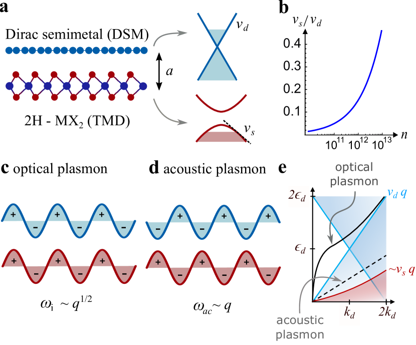
In this Letter, we propose a new route based on van der Waals (vdW) heterostructures Geim and Grigorieva (2013) in which a “sluggish” conductor with slow carriers serves as the polarizable medium to mediate attraction. Specifically, we propose a two-dimensional bilayer system consisting of a fast Dirac semimetal (DSM) layer, such as graphene, and a lightly doped semiconductor, such as Mo or W-based transition metal dichalcogenides (TMDs), to serve as the sluggish conductor, as schematically presented in Fig 1(a). Using a numerical solution of the Eliashberg equation, we perform a careful study of the transition temperature for realistic devices. From this analysis we conclude that Coulombic superconductivity is optimized by several parameters, for all of which our proposed vdW bilayers hold crucial advantages compared to traditional semiconductor double wells Vakili et al. (2004); Thakur et al. (1998):
(i) The ratio of the Fermi velocities of the two electronic systems must be very small, which is made possible in the vdW bilayer by the profound difference in electronic dispersion relations in the two layers [see Fig 1 (b)]. In this limit the resultant retarded attractive interaction satisfies the conditions for BCS theory.
(ii) The dielectric constant must be minimized in order to maximize the Coulomb interaction – a surrounding dielectric strongly suppresses . vdW layers are unique in their ability to be suspended Bolotin et al. (2008); Du et al. (2008); Weitz et al. (2010) and thus optimize the coupling strength, leading to experimentally relevant values (see Appendix C for details).
(iii) The distance between the electronic layers must be as small as possible in order to maximize their coupling. Also here, vdW heterostructures have a unique advantage by allowing for atomic-scale layer separations. We explore this in detail in Appendix D.
(iv) The strength of attraction is inversely proportional to the number of valleys in the fast layer. We analyze the transition temperature both for double-valley DSMs, such as graphene, as well as single valley DSMs. The latter obtains higher .
II Pairing from interlayer acoustic plasmons
To gain intuition for how the slow metallic layer serves to induce a retarded attractive interaction, we first discuss a limiting case in which we obtain analytic results. More rigorous numerical calculations estimating are presented in Section III. For all calculations, we consider the situation of a two-dimensional DSM placed on top of a lightly doped semiconducting TMD. Hereafter, we label the two layers by , corresponding to “DSM” and “semiconductor”, respectively.
II.1 Main concept
To understand better how such a device can convert Coulomb repulsion into attraction let us consider the dynamical picture of electronic screening. In the bilayer configuration, the long ranged Coulomb interaction gives rise to two collective plasma modes - resonances of the screened electron-electron interactions. As in BCS theory each such mode can in principle mediate an effective attractive interaction Takada (1980) if it is retarded with respect to the Fermi energy.
The first mode is the standard optical plasmon, which is the “in-phase” collective excitation of charge on the two layers [see Fig. 1 (c)]. Unless a strong dielectric medium surrounds the device, this mode is higher than the Fermi energy except for very small momentum transfer. In addition to this mode there is an acoustic plasma mode, which describes collective “out-of-phase” charge excitations of the two layers [see Fig. 1 (d)]. Because the charge modulation on one layer is canceled by a negative charge on the other, this mode is neutral and thus acoustic [the dispersion of the two modes and the particle-hole continuum are schematically presented in Fig. 1 (e)]. Thus, by adding the TMD layer, we effectively engineer an additional acoustic mode to the DSM, additive to the phonon modes. The coupling of this mode to the electrons in the DSM is, however, of different origin and may therefore be larger.
The long-wavelength velocity of the acoustic plasma mode is set by the geometric mean of the Fermi velocities of the two layers, and it is only weakly damped by its coexistence with the particle-hole continuum of the DSM. Specifically, for the limiting case of no separation between the layers () and equal densities, this mode disperses as , where , and
| (1) |
where is the ratio of band degeneracies, where and are the spin and valley degeneracies in layer , respectively (see Appendix A for details). For a DSM dispersing at m/s (equivalent to graphene) and a TMD with effective mass one can easily reach the limit where there are orders of magnitude between the Fermi velocity of the DSM and that of the TMD by tuning to the low density limit [see Fig. 1.(b)]. Thus, the BCS limit, in which the characteristic frequency of the acoustic mode is orders of magnitude smaller than the Fermi energy, is in reach. Moreover, unlike previous proposals based on parabolic bands Pashitskii (1969); Fröhlich (1968); Radhakrishnan (1965); Takada (1980); Entin-Wohlman and Gutfreund (1984); Garland (1963); Canright and Vignale (1989); Thakur et al. (1998), here the velocity ratio can be tuned over orders of magnitude by tuning the density. We also note that this mode was considered in early discussions of superconductivity in highly doped graphene Uchoa and Neto (2007). In Appendix F we discuss possible methods to observe the acoustic plasma mode in the normal state.
As explained, a key aspect in our proposal is the great difference in Fermi velocities. This implies that the mode disperses inside the particle hole continuum of the DSM and is therefore damped, leading to a finite in Eq. (1). It should be mentioned that the acoustic plasma mode is also often discussed in the context of double layers with similar velocities Santoro and Giuliani (1988); Hwang and Das Sarma (2009); Profumo et al. (2012a). In that case it disperses outside of the particle-hole continuum and is undamped, which makes it much more visible much less effective for superconductivity.
Finally, we note that the acoustic mode velocity in Eq. (1) does not depend on the Coulomb interaction. This is only an artifact of the limit, where the only restoring force is the quantum compressibility of the gases. For any finite layer separation the velocity will also depend on the parameters of the Coulomb interaction (see Appendix D).
II.2 The acoustic plasmon approximation
For concreteness, let us consider the limit of equal density in the two layers , where () is the Fermi momentum in the DSM (semiconductor) layer. The acoustic plasma mode described above separates two distinct regimes describing the Coulomb interaction within the DSM: at frequencies the TMD is too slow to respond and does not participate in screening of the Coulomb interaction, whereas for , the TMD adds to the total screening and suppresses the interaction by a significant amount. By taking an approximation in the vicinity of the acoustic plasma mode (see Appendix A.3 for details), we see that this manifests directly within the form of the Coulomb interaction at these two limits of high and low frequency:
| (2) | |||
| (3) |
where is the Thomas-Fermi wavevector of layer , is the dielectric constant and is the density of states per species. Indeed, one can see that the low-frequency interaction Eq. (3) has added screening by the TMD accounted for by its Thomas-Fermi wave-vector, as compared with the high-frequency case Eq. (2) where it is absent. The difference between these two limits, , is the attraction strength generated by the TMD layer at a given (for an equivalent scenario using polar optical phonons see Ref. Gurevich et al. (1962)). Note that both terms are positive (e.g. the Coulomb interaction is still repulsive at all frequencies), so this attraction strength is a relative measure. To obtain effective attraction at low energy the high frequency repulsion must be screened in the standard manner Morel and Anderson (1962) (see next subsection).
The above limiting forms for the interaction can be connected by inspecting the Coulomb interaction in the vicinity of the acoustic mode, where it takes the form
| (4) |
Here interpolates between the asymptotic behavior at high and low frequency [Equations (2) and (3)]. Eq. (4), as an approximation of the full interaction, neglects the dynamics of the polarization of the DSM (including the optical plasmon); henceforth, this approximation will be referred to as the acoustic plasmon approximation. Eq. (4) has been studied extensively in the context of multiband metals in which two bands with very different velocities are simultaneously occupied (see for example Refs. Pines (1956); Bennacer and Cottey (1989); Bennacer et al. (1989); Chudzinski and Giamarchi (2011)). It also has the same form as the well known phonon mediated interaction in the classic theory of superconductivity De Gennes (2018a). As a result, the acoustic plasmon has been proposed as a candidate mechanism for superconductivity by many authors in different contexts Pashitskii (1969); Fröhlich (1968); Radhakrishnan (1965); Takada (1980); Entin-Wohlman and Gutfreund (1984); Garland (1963); Canright and Vignale (1989); Thakur et al. (1998); Ruhman and Lee (2017).
Inspecting Eqs. (2-4), we find that the attraction strength, given by , becomes stronger as the ratio between the Thomas-Fermi momenta grows and the velocity ratio decreases. In this limit the velocity of the mode (1) also becomes highly retarded. The unique feature of the DSM-semiconductor bilayer, which makes it advantageous over previous proposals, is that the velocity ratio can be tuned and becomes infinite in the zero-density limit. Thus, the conditions for superconductivity are naturally optimized at low density.
II.3 Analytic calculation of within the acoustic plasmon approximation
Within BCS theory the resulting from (4) is determined by three parameters – the strength of the Coulomb pseudo-potential , the attraction strength , and the bandwidth of the acoustic mode (in phonon superconductivity this is the Debye frequency) – in the familiar form . To estimate and , let us assume pairing in the s-wave channel. When the Bloch bands are trivial these parameters are given by averaging the interaction over the Fermi surface Margine and Giustino (2013). In a DSM there is an additional coherence factor Ruhman and Lee (2017), where and are the incoming and outgoing momenta. Taking this factor into account, the bare Coulomb repulsion is given by
| (5) |
and the zero frequency attraction is
| (6) |
where . Finally, the bandwidth of the acoustic mode is estimated by .
The ratio quantifies the retardation and therefore controls the logarithmic screening of the instantaneous Coulomb repulsion (5) De Gennes (2018b)
| (7) |
Performing the integrals (5) and (6) we find that
| (8) |
After rewriting the bandwidth as , we come to our estimate for the transition temperature within the acoustic plasmon approximation:
| (9) |
The strength of the bare Coulomb repulsion (5) also sets the scale for the attraction (8) because they are both of the same origin.
In Fig. 2 we plot Eq. (9) as a function of the density () for different values of the DSM degeneracy: for the topological insulator (TI) surface state, for a spin-degenerate single-valley DSM, and for graphene. This quantity sets the strength of the bare Coulomb repulsion . We also set realistic estimates for the mass in a TMD monolayer, Fallahazad et al. (2016); Gustafsson et al. (2017), its degeneracy (corresponding to hole doping), and the velocity in existing DSMs .
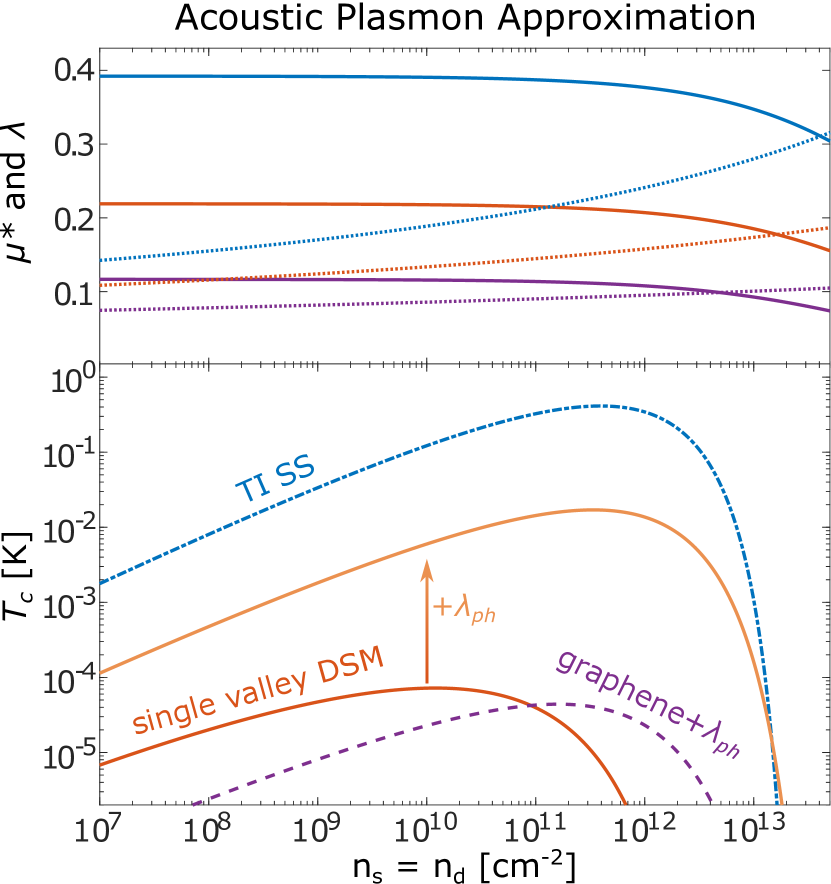
We expect the actual to be higher than estimated here due to three main factors:
(i) So far we have neglected the dynamical part of the DSM polarization. Once it is taken into account there is also a positive contribution from the optical plasmon that increases into a measurable range (see Section III).
(ii) Phonons in the DSM contribute to pairing in addition to the plasmonic modes. For example, in graphene the overall attraction due to phonons was estimated to be using first principles calculations Sun et al. (2014), which is a value typically insufficient to generate superconductivity. The phononic and plasmonic contributions are cooperative, and the total attraction can be as much as the sum of the two contributions if . To illustrate that this cooperation can have a substantial impact, we also plot the for the single- and double-valley DSMs with an added phonon contribution in Fig. 2, which increases by several orders of magnitude. A recent manuscript has explored this interplay for single-layer materials Roesner et al. (2018).
III Estimation of
III.1 Accounting for the full interaction
In the previous section we estimated transition temperatures (9) using the acoustic plasmon approximation. In this section, we estimate by more carefully accounting for the full dynamical and spatial form of both polarization functions. We use the linearized Eliashberg equation Takada (1992)
| (10) |
to compute numerically, where the vertex function is given by the angular average of the full interaction (again we assume s-wave pairing):
| (11) |
Here , is the angle between and , and is the full RPA interaction in the DSM layer (see Eq. 17). Note that in these equations we have switched to Matsubara frequencies, as the numerical solution is much simpler on the imaginary axis.
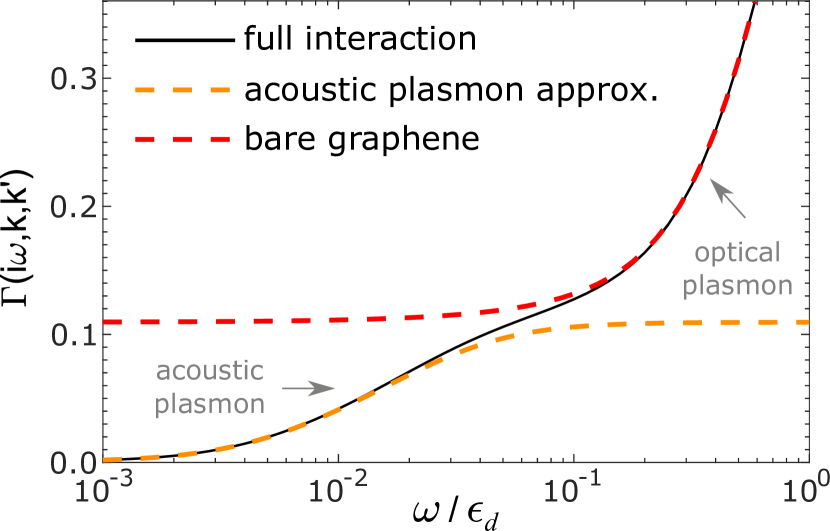
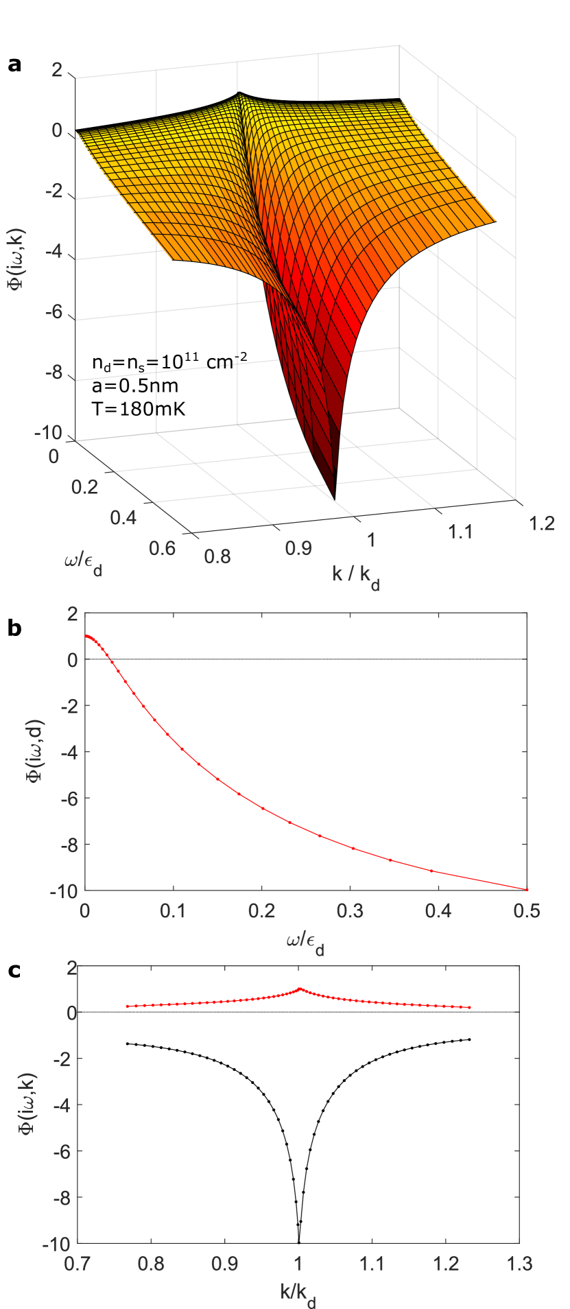
The vertex function (11) dictates . Therefore, it will be instructive to understand its properties before we discuss the results for the calculation of . In Fig. 3 we plot Eq. (11) as a function of frequency (solid black) for , , , , , , and 111The value of corresponds to suspended graphene.. monotonically decreases in two steps, occurring at the acoustic and optical mode frequencies (in real frequency these steps are resonances). Each such step represents an attractive contribution to the interaction. These contributions add up in Eq. (10). However, since the overall interaction is repulsive at all frequencies it is crucial that the high frequency repulsion gets renormalized. The upper cutoff of the frequency summation is thus a crucial phenomenological parameter affecting the transition temperature. We note that in our calculations the cutoff is never larger than the Fermi energy , and therefore the vertex function is plotted only up to that energy (see Appendix B for details).
It is important to contrast the full interaction (11) with two limiting cases. The first is the case of a bare DSM where there is no semiconducting layer, corresponding to the red dashed line in Fig. 3. In this case the drop at lower frequency is absent, and the overall value of the repulsive interaction in the limit is higher, which results in a weaker attraction at low energy. The second limit is the acoustic plasmon approximation (4) obtained by taking the polarization of the DSM to be a constant , represented by the dashed orange line in Fig. 3. In the range the interaction goes to a constant. Evidently, in this regime there are substantial deviations between this approximation (Eq. (4)) and the full interaction. These deviations contribute to elevate compared to Eq. (9) and are the effect of the optical plasmon.
III.2 Results for
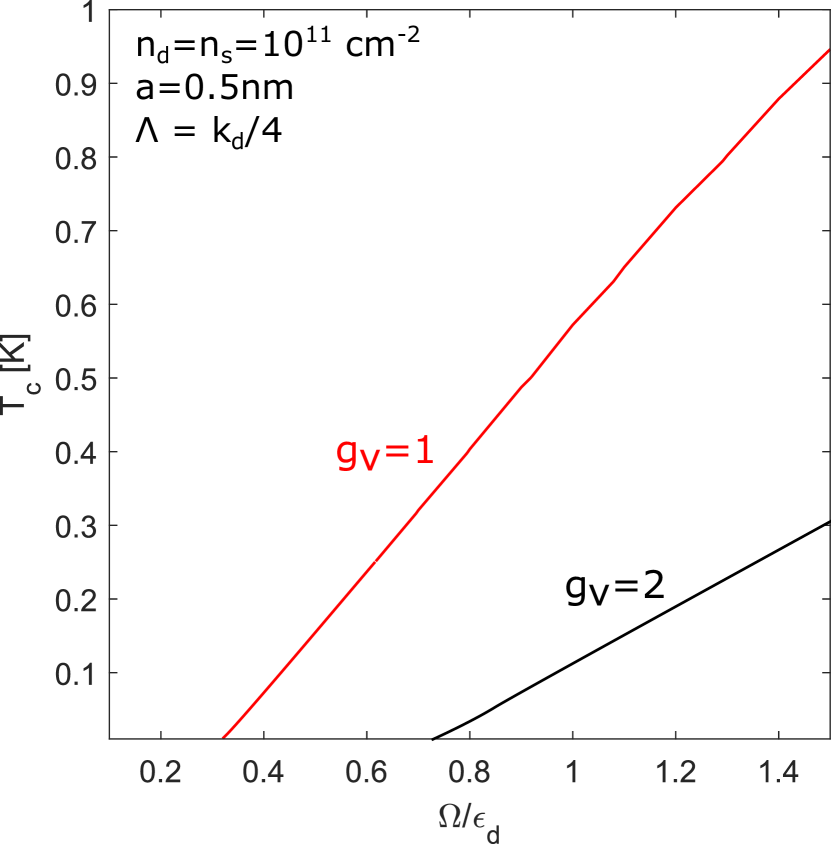
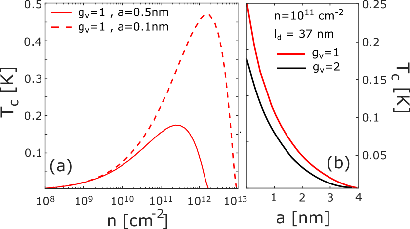
Let us now turn to the solution of obtained from solving Eq. (10). We account for a realistic separation between the center of the electronic wavefunctions in the vertical direction Ma et al. (2011), and we use as an estimate for the Thomas-Fermi wavevector of the DSM suspended in vacuum. The technical details of the numerical solution can be found in Refs. Takada (1992); Ruhman and Lee (2017) and in Appendix B. In Fig. 4 the transition temperature as a function of the density in the semiconducting layer, , is plotted for different values of the density in the DSM, , and for the case of one and two valleys (i.e. 1 and 2), corresponding to solid and dashed lines, respectively.
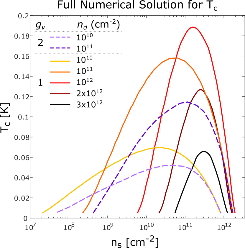
The transition temperature exhibits a dome shape, peaking at a non-universal value of the semiconductor density . It is interesting to note that the domes are wide on a logarithmic scale, such that the two layers may have significantly different densities without strongly affecting . The factors that dictate the suppression of for high and low are the following: in the limit , diminishes because the semiconductor is unable to screen at wavevectors of order . On the other hand, for the velocity ratio grows, thus harming the retardation condition. The peak is obtained by optimizing against these two parameters.
Before proceeding we would like to make a few comments. Here we have assumed the dielectric screening by the environment is negligible, i.e. we took . is very sensitive to this parameter and estimates of its effect are discussed in Appendix C. Second, the layer separation distance also has a strong effect on . Surprisingly, as we show in Appendix D, it becomes influential even when the interparticle distance is two orders of magnitude greater than the layer separation.
Finally, we comment that we have also used our calculation method to estimate the transition temperature in GaAs double quantum wells, where there is a large mass ratio between holes and electrons , which also quantifies the Fermi velocity ratio for equivalent layer density. This system was previously estimated to have a transition temperature of mK Thakur et al. (1998), but superconductivity was never observed. Indeed, we found that is immeasurably low, in agreement with prior calculations using the RPA Canright and Vignale (1989). This is due to the large dielectric screening and large layer separation as well as the inability to tune the effective mass ratio, an important advantage of our proposed DSM-semiconductor bilayer. For more details see Appendix E.
IV Conclusions
We have investigated the possibility that interlayer plasmons lead to superconductivity in vdW double layers. In particular we considered the scenario of a Dirac semimetal on top of a semiconducting transition metal dichalcogenide. Such a device has key advantages compared to previous proposals.
(i) First, the different nature of the dispersions in these systems allows for arbitrary tuning of the velocity ratio. The velocity ratio plays an important role, both in the strength of the coupling and in the scale of retardation.
(ii) Second, vdW devices can be suspended, placing them in an environment with the minimum possible dielectric constant and maximizing the Coulomb interaction strength.
(iii) Finally, vdW heterostructures allow for atomic-scale interlayer separations. As we discuss in Appendix D, drops with layer separation at a rate which is increased with coupling strength. Therefore, the ability to have atomic-scale interlayer separation is crucial in the limit of coupling strengths that lead to a measurable .
All of these parameters affect the pairing strength dramatically. We calculated numerically using the linearized Eliashberg equation. We found that in suspended devices of graphene on monolayer WSe2 a maximal transition temperature exceeding 100 mK can be achieved within a realistic density range. Moreover, we showed that can be substantially enhanced by pre-existing electron-phonon interactions Sun et al. (2014), and we argued that accounting for corrections to the compressibility of the electronic liquid at short distances would enhance the overall coupling Savary et al. (2017). can be further enhanced if the number of valleys is reduced, but realistic material candidates for these cases have yet to be verified.
V Acknowledgments
We are grateful to Avishai Benyamini, Justin Song, Patrick Lee, Marco Polini, and Hadar Steinberg for helpful discussions. JR acknowledges a fellowship from the Gordon and Betty Moore Foundation under the EPiQS initiative (grant no. GBMF4303).
Appendix A Model for the Bilayer System
A.1 Model Basics
We start from the dispersion Hamiltonian of the two layers, which is given by
| (12) | |||
| (13) |
where is a 4-component Dirac spinor in the basis of the Dirac matrices and and are the Dirac velocity and Fermi energy of the DSM. Equivalently, , , , and are the field operators, mass, Fermi energy, and Fermi velocity of the semiconducting layer. and are the corresponding Fermi momenta. For all calculations we use the exact .
A.2 Electronic Polarizations and Coulomb Interactions
The interactions between the layers generally have the form
| (14) |
where and are the density operators of the two layers. Within the random-phase-approximation (RPA) the matrix assumes the form Profumo et al. (2012b)
| (15) |
where is the separation between the two layers [see Fig. 1 (a)] and the factor in the denominator is given by
The bare Coulomb interaction is given by , where is a uniform dielectric constant. The polarization functions of the two layers are given by , where take into account any possible valley or spin degeneracies, is the density of states per species and the functions are well known Barlas et al. (2007)
where and . Note that here, for the polarization of the DSM, we have taken both the interband and intraband contributions to the polarization.
Overall the interlayer interaction within the DSM, which we use in the Eliashberg equation (11), is given by
| (17) |
In the limit of we obtain Eq. (18), and in the limit of we restore the single layer result. Notice, however, that the exponential factor controlling the crossover between these two limits is . Thus, the appropriate length scale one must consider when comparing with the interparticle distance is not rather than .
A.3 Details of the Acoustic Plasmon Approximation
For simplicity, let us assume the density per flavor in each layer is equal, i.e. . Furthermore, let us assume for a moment that the distance between the layers is much smaller than the interparticle distance, i.e. . In this case we may assume that for all relevant momenta and thus the interaction (17) assumes the simple form
| (18) |
where is the Thomas-Fermi wavelength of layer .
The ratio between the Fermi velocities is given by , and thus approaches zero in the low density limit [see Fig. 1(b) for realistic values]. Consequently, the frequency window becomes parametrically large in the low density limit, which allows for the following approximations to the polarization functions:
| (19) |
From these approximations to the polarization functions, we can find the pole that gives the acoustic plasma mode given by Eq. (1) and reduce the full interaction to the acoustic plasmon approximation given in Eq. (4).
Appendix B Details of the numerical solution of the linearized Eliashberg equation
The technique we have used here to solve for was first introduced by Takada Takada (1992) and is detailed in Ref. Ruhman and Lee (2017). Eq. (10) is obtained from neglecting mass renormalization and dispersion corrections, and then linearizing the Eliashberg equation Eliashberg (1960); Margine and Giustino (2013) for the order parameter. Then the sum over frequencies and momenta is truncated at the cutoffs and , respectively. Here we always limit the frequency cutoff by the Fermi energy, i.e. .
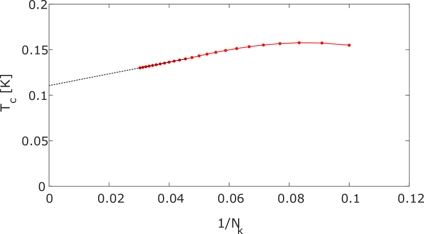
In the next step only a subset of Matsubara frequencies and momenta points are chosen. The number of such points is labeled by and . We set . Finally, the distribution of points is taken to be denser near the first Matsubara frequency and the Fermi surface . We choose an algebraically diverging density of points and . For all simulations we take and .
is then obtained by seeking the value of , to which the kernel on the r.h.s. of Eq. (10) has a unity eigenvalue. Note that this must be the largest (positive) eigenvalue. The corresponding eigenvector at mK, , and nm is plotted in Fig. 5(a). Note that this represents the gap at such that the overall scale of the gap is arbitrary [we chose to normalize by ].
The dependence on frequency is plotted in Fig. 5(b) for . As in the standard theory of superconductivity we find that the gap function changes sign at the frequency of the acoustic plasmon mode (in this case ). In Fig. 5(c) the momentum dependance of the gap function is plotted for two frequencies: (red) and (black). The sharp feature near is captured by the appropriate density of points controlled by .
The dependence of on the frequency cutoff is presented in Fig. 6. is found to be mostly linear in the cutoff in the range of interest. We point out that this is not inconsistent with the standard formula for in the weak coupling limit (e.g. Eq. 9) where the cutoff tunes the parameter Morel and Anderson (1962); Margine and Giustino (2013). As such, the cutoff must be considered as a phenomenological parameter. Since Eliashberg theory, which is based on the sum over Gor’kov ladder diagrams, is justified only at low energy compared to we insist that the cutoff must not be larger than . In doing so, we differ from previous studies (e.g. Refs. Takada (1980); Canright and Vignale (1989)) by taking this more conservative approach.
The dependence of the transition temperature with the number of points in momentum space is plotted in Fig. 7. As can be seen the transition temperature decreases slowly towards the thermodynamic limit but clearly converges to a finite value.
We also note that at sufficiently low temperatures the Eliashberg equation predicts a small but finite even in the case of a single two-dimensional metallic layer due to the optical plasmon, as pointed out by Takada long ago Takada (1978). In the whole parameter range we have studied here this temperature is lower than 5 mK, which is the minimal temperature in our numerical simulation.
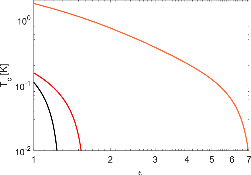
Appendix C Effect of dielectric screening
In the main text we have assumed a vacuum dielectric constant of . In this section we compute the effects of finite dielectric screening. In Fig. 8 we plot vs. the dielectric constant for , and the case of a 3D topological insulator (TI) surface state (). is much larger in the last case: K for and becomes immeasurably small at around . This plot shows that superconductivity is extremely sensitive to the dielectric environment surrounding the device. It is however, important to note that in the case where only a half plane is polarizable this value corresponds to half of the bulk value of . Finally, we note that the large in the TI surface states naively makes them the most promising candidates to realize plasmonic superconductivity. However, all known realizations of the 3D TIs also have a huge dielectric constant.
Appendix D Effect of layer separation
In the main text we have assumed the minimum possible layer separation nm. In this section we compute the effects of modifying the layer separation. In Fig. 9(a) we plot for single valley DSMs as a function of density (solid curves) for the case of , where all other parameters are as in Fig. (4). As before we find that exhibits a dome as a function of total density. At extremely low density the two curves coincide signaling that the effects of modifying the layer separation from nm to nm vanishes when the interparticle distance is big enough. In this limit drops because the overall scale for the acoustic plasmon decreases. On the other hand, the main factor that suppresses in the high density limit is the finite separation between the layers, . This can be seen by comparing the nm (solid) curve to the (dashed). The latter has a finite up to much higher density values.
To further clarify this point we plot as a function of the layer separation, , for in Fig. 9(b). Interestingly, is strongly affected by layer separation on the scale despite the very large interparticle separation ( nm). Thus, to avoid significant suppression of the transition temperature the layer separation must be smaller than the interparticle distance by almost two orders of magnitude.
We can understand the high sensitivity to layer separation by inspecting the coupling constant for the interaction (17), finding that it is reduced linearly in : . Note that, for suspended graphene, . Thus, the more stringent requirement is apparent, indicating the interplay of these length-scales with the Coulomb interaction. This also implies that as the coupling becomes stronger the sensitivity to layer separation becomes greater.
It was also mentioned in the main text that the velocity of the acoustic mode can acquire additional stiffness due to Coulomb interactions at finite layer separation . This can be quantified by solving for the pole of the acoustic plasma mode for small . In this limit, we find
| (20) |
So again the layer separation plays an important role, although less so than in the coupling constant.
Appendix E The case of GaAs double wells
Superconductivity from interlayer plasmons has been proposed in the past in the context of electron-hole double layer quantum wells in GaAs Vakili et al. (2004). A transition temperature of 100 mK was estimated Thakur et al. (1998), but superconductivity was never observed experimentally. To make a comparison with these previous predictions, we checked the prediction of Eq. (10) with the same parameters as in Ref. Thakur et al. (1998); however, we did not find a superconducting instability for mK.
For this calculation, we took two single valley parabolic bands with equal and opposite density of , the masses are taken to be and , and nm. Otherwise, we used the same numerical parameters that were used to generate Fig. 4, except for the cutoff , which in this case we took to be higher, namely equal to the Fermi energy of the electron band (with the higher Fermi energy of the two).
is suppressed in the GaAs double wells mainly because the mass ratio, is not large enough, the dielectric environment strongly screens the interaction, and the quantum wells are relatively far apart. This highlights the several advantages of DSM-semiconductor double layers based on van der Waals materials: there is no theoretical bound on the effective mass ratio (or more accurately on the velocity ratio); the electronic system can be subjected to a more variable dielectric environment; and the interlayer separation can be taken to be much smaller.
Appendix F Non-superconducting indicators of the acoustic plasma mode
In the main text we investigated the possibility that the acoustic plasma mode in DSM-semiconductor bilayers leads to a superconducting instability. We would like to emphasize, however, that the experimental observation of this mode, even without superconductivity, is of fundamental interest. To the best of our knowledge such a mode was never observed in the limit of such a large velocity ratio, wherein the mode lies in the particle-hole continuum. Similar physics was found for surface plasmons on 3d metals Diaconescu et al. (2007); Lundeberg et al. (2017) as well as for photoexcited 3d semiconductors Padmanabhan et al. (2014). Moreover, it will be important to verify that the acoustic plasma mode exists in DSM-semiconductor bilayers in addition to the search for the superconductivity.
Transport – The existence of a low energy acoustic mode was predicted to lead to phonon like scattering Chudzinski and Giamarchi (2011) and thus contribute to resistivity. In the case of two-dimensions this scattering mechanism should lead to a contribution , where the energy scale is proportional to and is therefore density dependent. It is important to note that such a contribution can only appear if the momentum decay rate of the acoustic plasma mode to impurities is much greater than to electrons. Another transport indicator of the acoustic plasmon is expected in the interlayer Coulomb drag signal. Here a distinctive non-monotonic temperature dependance has been predicted Flensberg and Hu (1994).
Tunneling – We also expect that the acoustic plasmon can be measured using inelastic tunneling between the layers de Vega and García de Abajo (2017). Plasmonic spectroscopic signatures have been measured in GaAs quantum wells Jang et al. (2017) and high quality tunneling data can be achieved by using van der Waals layers as a tunnel barrier Dvir et al. (2018). It would also be interesting if the scanning near field probes could find a method to couple to this mode Fei et al. (2012); Alonso-González et al. (2016). However, it is important to note that because of the small layer separation , the dipole moment of the mode is expected to be extremely small.
Optics – The acoustic plasmon is essentially a longitudinal mode involving the relative charge oscillations on the two layers. As such it can be measured using Raman spectroscopy, as demonstrated in GaAs quantum wells Bhatti et al. (1996); Kainth et al. (1998, 1999).
Plasmon - phonon interaction – Finally, the acoustic plasmon is allowed to couple to other longitudinal waves, such as acoustic and optical phonons. At points where the dispersion branches cross, strong phonon-plasmon coupling is expected. However, it is important to note that even in the extremely dilute limit the velocity of the acoustic plasmon is expected to be larger than the acoustic phonon velocity in graphene.
References
- Little (1964) W. A. Little, Physical Review 134 (1964), 10.1103/PhysRev.134.A1416.
- Ginzburg (1964) V. L. Ginzburg, Physics Letters 13, 101 (1964), arXiv:1412.0460 .
- Allender et al. (1973) D. Allender, J. Bray, and J. Bardeen, Phys. Rev. B 7, 1020 (1973).
- Bardeen (1978) J. Bardeen, Journal of The Less-Common Metals 62, 447 (1978).
- Merlin (1990) R. Merlin, Solid State Communications 75, 743 (1990).
- Gutfreund and Little (1996) H. Gutfreund and W. Little, in From High-Temperature Superconductivity to Microminiature Refrigeration (Springer, 1996) pp. 65–132.
- Malozovsky and Fan (1996) Y. Malozovsky and J. Fan, Superconductor Science and Technology 9, 622 (1996).
- Cotleţ et al. (2016) O. Cotleţ, S. Zeytinoǧlu, M. Sigrist, E. Demler, and A. m. c. Imamoǧlu, Phys. Rev. B 93, 054510 (2016).
- Kavokin and Lagoudakis (2016) A. Kavokin and P. Lagoudakis, Nature Publishing Group 15, 599 (2016).
- Hamo et al. (2016) A. Hamo, A. Benyamini, I. Shapir, I. Khivrich, J. Waissman, K. Kaasbjerg, Y. Oreg, F. Von Oppen, and S. Ilani, Nature 535, 395 (2016).
- Morel and Anderson (1962) P. Morel and P. W. Anderson, Phys. Rev. 125, 1263 (1962).
- Geim and Grigorieva (2013) A. K. Geim and I. V. Grigorieva, Nature 499, 419 (2013).
- Vakili et al. (2004) K. Vakili, Y. P. Shkolnikov, E. Tutuc, E. P. De Poortere, and M. Shayegan, Physical Review Letters 92, 90 (2004), arXiv:0309385v1 [arXiv:cond-mat] .
- Thakur et al. (1998) J. Thakur, D. Neilson, and M. Das, Physical Review B 57, 1801 (1998).
- Bolotin et al. (2008) K. I. Bolotin, K. Sikes, Z. Jiang, M. Klima, G. Fudenberg, J. Hone, P. Kim, and H. Stormer, Solid State Communications 146, 351 (2008).
- Du et al. (2008) X. Du, I. Skachko, A. Barker, and E. Y. Andrei, Nature nanotechnology 3, 491 (2008).
- Weitz et al. (2010) R. T. Weitz, M. T. Allen, B. E. Feldman, J. Martin, and A. Yacoby, Science 330, 812 (2010).
- Takada (1980) Y. Takada, Journal of the Physical Society of Japan 49, 1713 (1980).
- Pashitskii (1969) E. A. Pashitskii, Soviet Physics JETP 28, 1267 (1969).
- Fröhlich (1968) H. Fröhlich, Journal of Physics C: Solid State Physics 1, 544 (1968).
- Radhakrishnan (1965) V. Radhakrishnan, Physics Letters 16, 247 (1965).
- Entin-Wohlman and Gutfreund (1984) O. Entin-Wohlman and H. Gutfreund, Journal of Physics C: Solid State Physics 17, 1071 (1984).
- Garland (1963) J. W. Garland, Phys. Rev. Lett. 11, 111 (1963).
- Canright and Vignale (1989) G. S. Canright and G. Vignale, Physical Review B 39, 2740 (1989).
- Uchoa and Neto (2007) B. Uchoa and A. C. Neto, Physical Review Letters 98, 146801 (2007).
- Santoro and Giuliani (1988) G. E. Santoro and G. F. Giuliani, Phys. Rev. B 37, 937 (1988).
- Hwang and Das Sarma (2009) E. H. Hwang and S. Das Sarma, Phys. Rev. B 80, 205405 (2009).
- Profumo et al. (2012a) R. E. V. Profumo, R. Asgari, M. Polini, and A. H. MacDonald, Phys. Rev. B 85, 085443 (2012a).
- Gurevich et al. (1962) L. V. Gurevich, A. I. Larkin, and Y. A. Firsov, Sov. Phys. Sol. State 4, 131 (1962).
- Pines (1956) D. Pines, Canadian Journal of Physics 34, 1379 (1956).
- Bennacer and Cottey (1989) B. Bennacer and A. Cottey, Journal of Physics: Condensed Matter 1.10, 1809 (1989).
- Bennacer et al. (1989) B. Bennacer, A. Cottey, and J. Senkiw, Journal of Physics: Condensed Matter 1.45, 8877 (1989).
- Chudzinski and Giamarchi (2011) P. Chudzinski and T. Giamarchi, Physical Review B 84, 125105 (2011).
- De Gennes (2018a) P.-G. De Gennes, Superconductivity of metals and alloys (CRC Press, 2018).
- Ruhman and Lee (2017) J. Ruhman and P. A. Lee, Phys. Rev. B 96, 235107 (2017).
- Margine and Giustino (2013) E. R. Margine and F. Giustino, Phys. Rev. B 87, 024505 (2013).
- De Gennes (2018b) P.-G. De Gennes, Superconductivity of metals and alloys (CRC Press, 2018).
- Fallahazad et al. (2016) B. Fallahazad, H. C. P. Movva, K. Kim, S. Larentis, T. Taniguchi, K. Watanabe, S. K. Banerjee, and E. Tutuc, Phys. Rev. Lett. 116, 086601 (2016).
- Gustafsson et al. (2017) M. V. Gustafsson, M. Yankowitz, C. Forsythe, D. Rhodes, K. Watanabe, T. Taniguchi, J. Hone, X. Zhu, and C. R. Dean, “Ambipolar landau levels and strong band-selective carrier interactions in monolayer wse2,” (2017), arXiv:1707.08083 .
- Sun et al. (2014) Q.-c. Sun, Y. Ding, S. M. Goodman, H. H. Funke, and P. Nagpal, Nanoscale 6, 12450 (2014).
- Roesner et al. (2018) M. Roesner, R. Groenewald, G. Schoenhoff, J. Berges, S. Haas, and T. Wehling, arXiv preprint arXiv:1803.04576 (2018).
- Savary et al. (2017) L. Savary, J. Ruhman, J. W. F. Venderbos, L. Fu, and P. A. Lee, Phys. Rev. B 96, 214514 (2017).
- Takada (1992) Y. Takada, Journal of the Physical Society of Japan 61, 238 (1992).
- Note (1) The value of corresponds to suspended graphene.
- Ma et al. (2011) Y. Ma, Y. Dai, M. Guo, C. Niu, and B. Huang, Nanoscale 3, 3883 (2011).
- Profumo et al. (2012b) R. E. V. Profumo, R. Asgari, M. Polini, and A. H. MacDonald, Phys. Rev. B 85, 085443 (2012b).
- Barlas et al. (2007) Y. Barlas, T. Pereg-Barnea, M. Polini, R. Asgari, and A. H. MacDonald, Phys. Rev. Lett. 98, 236601 (2007).
- Eliashberg (1960) G. M. Eliashberg, Sov. Phys. Sol. JETP 11, 696 (1960).
- Takada (1978) Y. Takada, Journal of the Physical Society of Japan 45, 786 (1978).
- Diaconescu et al. (2007) B. Diaconescu, K. Pohl, L. Vattuone, L. Savio, P. Hofmann, V. M. Silkin, J. M. Pitarke, E. V. Chulkov, P. M. Echenique, D. Farias, et al., Nature 448, 57 (2007).
- Lundeberg et al. (2017) M. B. Lundeberg, Y. Gao, R. Asgari, C. Tan, B. Van Duppen, M. Autore, P. Alonso-González, A. Woessner, K. Watanabe, T. Taniguchi, et al., Science , eaan2735 (2017).
- Padmanabhan et al. (2014) P. Padmanabhan, S. M. Young, M. Henstridge, S. Bhowmick, P. K. Bhattacharya, and R. Merlin, Phys. Rev. Lett. 113, 027402 (2014).
- Flensberg and Hu (1994) K. Flensberg and B. Y.-K. Hu, Phys. Rev. Lett. 73, 3572 (1994).
- de Vega and García de Abajo (2017) S. de Vega and F. J. García de Abajo, ACS Photonics 4, 2367 (2017).
- Jang et al. (2017) J. Jang, H. M. Yoo, L. Pfeiffer, K. West, K. Baldwin, and R. C. Ashoori, Science 358, 901 (2017).
- Dvir et al. (2018) T. Dvir, F. Massee, L. Attias, M. Khodas, M. Aprili, C. H. Quay, and H. Steinberg, Nature Communications 9, 598 (2018).
- Fei et al. (2012) Z. Fei, A. Rodin, G. Andreev, W. Bao, A. McLeod, M. Wagner, L. Zhang, Z. Zhao, M. Thiemens, G. Dominguez, et al., Nature 487, 82 (2012).
- Alonso-González et al. (2016) P. Alonso-González, A. Y. Nikitin, Y. Gao, A. Woessner, M. B. Lundeberg, A. Principi, N. Forcellini, W. Yan, S. Vélez, A. J. Huber, et al., Nature nanotechnology (2016).
- Bhatti et al. (1996) A. S. Bhatti, D. Richards, H. P. Hughes, and D. A. Ritchie, Phys. Rev. B 53, 11016 (1996).
- Kainth et al. (1998) D. S. Kainth, D. Richards, H. P. Hughes, M. Y. Simmons, and D. A. Ritchie, Phys. Rev. B 57, R2065 (1998).
- Kainth et al. (1999) D. S. Kainth, D. Richards, A. S. Bhatti, H. P. Hughes, M. Y. Simmons, E. H. Linfield, and D. A. Ritchie, Phys. Rev. B 59, 2095 (1999).