Large scale low power computing system
Abstract
The deployment of the next generation computing platform at ExaFlops scale requires to solve new technological challenges mainly related to the impressive number (up to ) of compute elements required. This impacts on system power consumption, in terms of feasibility and costs, and on system scalability and computing efficiency. In this perspective analysis, exploration and evaluation of technologies characterized by low power, high efficiency and high degree of customization is strongly needed. Among the various European initiative targeting the design of ExaFlops system, ExaNeSt and EuroExa are EU-H2020 funded initiatives leveraging on high end MPSoC FPGAs. Last generation MPSoC FPGAs can be seen as non-mainstream but powerful HPC Exascale enabling components thanks to the integration of embedded multi-core, ARM-based low power CPUs and a huge number of hardware resources usable to co-design application oriented accelerators and to develop a low latency high bandwidth network architecture.
In this paper we introduce ExaNet the FPGA-based, scalable, direct network architecture of ExaNeSt system. ExaNet allow us to explore different interconnection topologies, to evaluate advanced routing functions for congestion control and fault tolerance and to design specific hardware components for acceleration of collective operations. After a brief introduction of the motivations and goals of ExaNeSt and EuroExa projects, we will report on the status of network architecture design and its hardware/software testbed adding preliminary bandwidth and latency achievements.
keywords:
ExaScale\sepHigh Performance Computing\sepNetwork\sepInterconnect\sepThe final publication is available at IOS Press through
http://dx.doi.org/10.3233/978-1-61499-843-3-750
(2018) Advances in Parallel Computing, 32, pp. 750-759, Talk at ParCo 2017.
and
1 Introduction
The next generation HPC systems will be characterized by ExaFlops performances — i.e. Floating Point Operations per second — and will be used in a broad class of large size, computing-demanding scientific and industrial applications, ranging from modeling and simulation of complex physical systems to biotechnology, cloud computing, big data and analytics.
At a very high level of abstraction, an ExaFlops-scale HPC system will be composed of something in the order of millions of computing cores. A simple system power estimation, based on current state-of-the-art technologies and compute elements, yields a total power consumption of MW which is a factor 510 more than what is generally agreed as the maximum possible for a single data center site.
So, if in the past the challenge was to achieve the floating point performance target with the minimal number of computing components and limited procurement costs, today the computing efficiency, the power consumption and the system cooling have become key factors driving HPC design. In this perspective, the next generation one-million cores HPC systems have to adopt low power CPUs, co-design and integrate application-oriented computing accelerators, build new cooling mechanics while designing scalable, low latency, high performance interconnection architectures suitable for such as extreme scale systems.
In this paper we describe the architecture and the FPGA implementation of ExaNet, a novel network architecture targeted for Exascale HPC systems which is under design in the framework of H2020 EU-funded projects, ExaNeSt and EuroExa, whose motivations and goals are described in section 2. Section 3 details the ExaNet architecture and hardware implementation while section 4 describes the KARMA test framework, discussing power consumption estimations and preliminary latency and bandwidth test results.
2 Designing European ExaScale systems: ExaNeSt and EuroExa H2020 project
In the last 5 years a number of EU-funded initiatives were launched, trying to reduce the technological gap between European and extra-European HPC systems. Leveraging on ARM architectures, the Mont-Blanc series of projects [1] has paved the way towards an HPC system based on low power CPUs while the UniServer [2] project has designed a scalable platform based on ARM-based microservers.
The ExaNeSt [3] project, started on December 2015 and funded in EU H2020 research framework (call H2020-FETHPC-2014, n. 671553), is a pillar of a larger initiative that includes ExaNode [4] and EcoScale [5] projects and aims to demonstrate the efficient usage of low power architectures in Exascale computing platforms. ExaNode focuses on delivering a novel, highly power-efficient compute element for HPC and EcoScale deploys a full software stack needed to use high-end FPGAs as accelerators for HPC systems. Furthermore, ExaNeSt combines industrial and academic research expertise to design the architecture and deploy a fully functional demonstrator of an innovative system-level interconnect, distributed NVM (Non-Volatile Memory) storage and advanced cooling infrastructure for an ARM-based ExaFlops-class supercomputer.
One of the main goals within ExaNeSt is the design of ExaNet: a novel, unified (for data and storage traffic), low latency, high throughput, RDMA-based interconnect architecture suitable for extreme scale system. The project leans on last generation high end SoC (System on Chip) FPGAs — the Xilinx Zynq UltraScale+[6] with 4 ARM Cortex-A53 embedded cores running at up to — to integrate thousands of cores into a fully working system prototype.
Starting in September 2017, a new H2020 EU initiative named EuroExa [7] — funded under the FETHPC-2016 program (call H2020-FETHPC-2016, n. 754337) — will build upon ExaNeSt results to deliver a world-class, ARM-based HPC platform prototype. The main deliverable of the project is a co-designed platform capable of scaling to a peak performance to 400 PFlops in a system with a peak power envelope of 30 MW achieved through a customized ARM-based processing unit, the adoption of FPGAs for data-flow acceleration and the integration at rack level of a low latency, high throughput ExaNet-based network architecture.
3 ExaNet
ExaNet is responsible for data communication at Tier 0/1/2 of the network interconnect of the ExaNeSt project. ExaNet is the product of a joint collaboration among the Foundation for Research and Technology (FORTH) in Greece and Istituto Nazionale di Fisica Nucleare (INFN) in Italy. The INFN APE Research group, which in the past has designed the APEnet [8] 3D-Torus network architecture, is responsible for the ExaNet Network IP that provides switching and routing features and manages the communication over the High Speed Serial (HSS) links through different levels of the ExaNeSt interconnect hierarchy:
-
•
the high-throughput intra-QFDB level (Tier 0) for data transmission among the four FPGAs of the ExaNeSt node;
-
•
the intra-Mezzanine level (Tier 1) directly connecting the network FPGAs of different nodes within the same mezzanine;
-
•
inter-Mezzanine communication level (Tier 2) managing the connectivity of the Mezzanine based on SFP+ connectors and allowing for the implementation of a direct network among QFDBs within a Chassis.
The ExaNet Network IP mainly consists of two hardware components:
3.1 ExaNet development platform.
Being the early stages of the ExaNeSt project, the current ExaNet release was designed on a Trenz [9] TEBF0808 system, featuring the same Xilinx Ultrascale+ MPSoC FPGA family chosen for the final prototype (XCZU9EG). Preliminary tests were performed to validate the network, connecting up to four boards shaping a mesh topology through the two SFP+ connectors available on each Trenz system.
The testbed allows to validate the adoption of the APEnet architecture at both Tier 0 and Tier 1. The QFDB composed by four FPGAs matches perfectly with the testing platform. Furthermore, the development platform emulates the communication among the four network FPGAs of the QFDBs hosted within the track-1 mezzanine.
3.2 Packet structure
A modified version of the APEpacket is the data structure of the ExaNet communication system based on the latest generation of the APEnet protocol. Figure 1 outlines the ExaNet packet.

The packet is composed by a 128-bit header, a 128-bit footer and a payload. The maximum payload size is bytes, being a good compromise between bandwidth performances and routing efficiency (to avoid delaying high priority packets).
3.3 APErouter
The APErouter block dynamically interconnects the intra-tile ports — i.e. the interface between the programming logic and the programming subsystem — and inter-tile ports — i.e. the I/O interface with the other nodes — and comprises a fully connected switch, plus routing and arbitration blocks.
The current release of the APErouter is targeted to Xilinx devices and is compliant with the ExaNet Header format. It manages different kinds of packets and supports byte-aligned data structures in memory — the previous releases were word-aligned. The design has been tuned to evaluate different network topologies and to explore the introduction of new features — adaptive routing algorithms and hardware acceleration of collective functions.
Although the basic functionalities of the APErouter were verified in the past — on the QUonG [10] prototype located in Rome — correct behaviour of the new release is currently under test on the mini-cluster composed by Trenz boards described in Section 3.1. Single- and multiple-hop tests were performed and the results are shown in Section 4 and Section 4.3.
The block diagram of the APErouter is depicted in Figure 2.
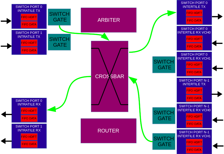
The bidirectional Switch Port contains transmitting (TX) and receiving (RX) FIFOs. The header/footer FIFOs are bit (2 KB), while the intra-tile and inter-tile payload FIFO are bit (64 KB) and bit (16 KB) respectively.
The Switch Gate connects data and control signals coming from the intra-tile and inter-tile ports with the crossbar. It manages the data flow preventing FIFOs overflow and guarantees proper transmission of the packet sequence — header, payload, footer.
The Router applies a deterministic Dimension-Ordered Routing (DOR) policy consisting in reducing to zero the offset between current and destination node coordinate along one dimension before considering the offset in the next dimension. The router is able to simultaneously handle more than one packet transaction. Specialized priority registers allow selecting the coordinates evaluation order — i.e. first Z is consumed, then Y and finally X — and disabling ports altogether. The implemented switching technique is Virtual Cut-Through [11] (VCT): the router starts forwarding the packet as soon as the algorithm has picked a direction and the buffer used to store the packet has enough space. The DOR algorithm, not per-se deadlock-free, is made as such by the implementation of two virtual channels for each physical channel; the router sends packets using the upper virtual channel if the offset between current and destination node is greater than zero, the lower virtual channel otherwise.
The Arbiter manages conflicts among the requests, granting ordered access to packets coming from different ports that request the same destination port. The scheduling algorithm is configurable: Round Robin or Fixed priority — the latter can be modified at run-time writing the proper configuration register.
3.4 APElink
Packet payload is encapsulated in a lightweight protocol sketched in Figure 1. Two words — Magic/Start — are included into the data flow over the serial links to frame the packet boundaries and announce the transmission of the Header; their transmission takes 2 clock cycles only.
Since misrouted packets are disruptive for the network, the highly critical header integrity is protected by an Error Correction Code (ECC). Payload integrity is guaranteed by a CRC32 code. APElink does not provide any acknowledgement or retransmission mechanism, to not affect performance of the transmission forcing the implementation of additional memory buffers.
Buffer availability is measured by credit; exchanging credits by two communicating nodes is mandatory to avoid buffer overflow. Outbound words consume it, causing transmission suspension as soon as a programmable credit threshold (TRED) is reached –– i.e. credit is exhausted –– and resuming as soon as info about newly available space bounces back to the transmitter –– i.e. credit is eventually restored. This information is exploited by the router to manage the data flow implementing the VCT switching mechanism.
Besides, some information regarding the health of the node can be optionally embedded in the credits, allowing for a fault communication mechanism — LO|FA|MO [12] — that avoids single points of failure and guarantees a fast broadcast of critical status to neighboring nodes. This embedding of diagnostic messages in the communication protocol limits the amount of additional overhead (no custom diagnostic packets are necessary) and prevents this flow from affecting overall performance.
3.4.1 APElink hardware IP
The APElink hardware IP manages the communication protocol over the serial links, adapting the inter-tile port interface of the APErouter with the outbound interface of the network adapter. The APElink IP consists of two main components: (i) the Transmission Control Logic (TCL), a totally FPGA vendor-independent IP, that manages data and credit flow over the link (OSI Data Link, APElink) and (ii) the Transceiver, provided by the FPGA vendor and configured to fit the design requirements, implements the OSI Physical layer, APEphy).
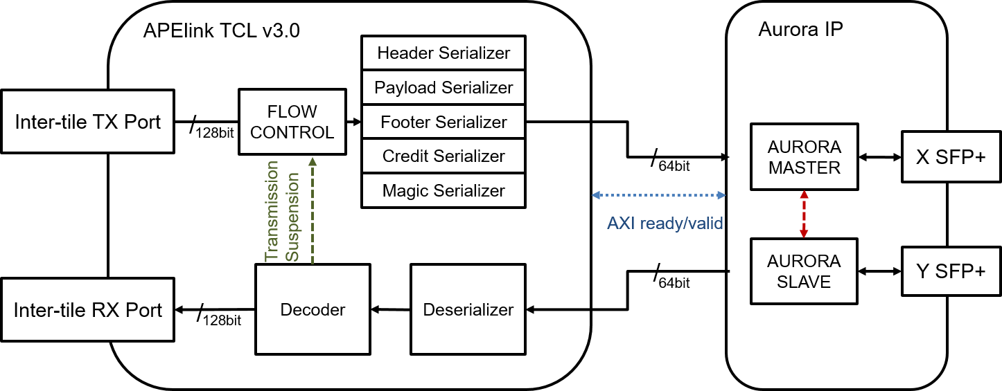
The interface between TCL and Transceiver is based on a standard Ready/Valid mechanism, to be compliant with the AXI stream protocol and to increase the compatibility of the APElink hardware component with different FPGA vendor IPs or custom transceiver controllers. The block diagram of current ExaNet APElink data transmission system is shown in Figure 3.
The transceiver IP is based on Xilinx Aurora 64B/66B core. Aurora 64B/66B is a lightweight, serial communications protocol for multi-gigabit links. It is used to transfer data between devices using one or many GTH transceivers.
4 KARMA Test Framework
King ARM Architecture (KARMA) is a software-oriented test framework to validate the ExaNet Network IP. The main idea behind its design is the use of the multicore ARM Cortex-A53 Programming System (PS) to emulate in software the functionalities of the Network Interface (NI), exploiting the AXI low latency communication capabilities between the PS and the Programming Logic (PL) that implements the system under test. This approach turned out to be very effective, allowing for test and validation of the ExaNet Network IP since the earliest stages of its development. It also enabled the rapid prototyping of various architectural solutions for the interface between the NI and the Switch systems. Finally, using the framework we were able to characterize the performance of the two systems in terms of latency.

On the hardware side, the intra-tile ports are directly connected to the ARM HPM AXI port through an adapter IP, whose only purpose is the conversion between streaming and memory-mapped AXI protocols.
Current KARMA does not implement any DMA-access to the intra-tile ports, so that ARM must issue a write for every single word into header/data FIFOs, which is obviously suboptimal for bandwidth but appropriate for gauging the latency of small-sized packets.
Moreover, a set of configuration/status registers is accessible on the same AXI bus through the “Target Controller” IP, which allows configuration of the router (e.g. setting coordinates and lattice size) and probing FIFOs and link status.
An overview of the KARMA test framework is depicted in Figure 4, where the ExaNet Network IP— i.e. APErouter and two APElink Transmission Control Logic blocks and Target Controller — is the device under test. Its operating frequency jointly with the APEphy, composed by the FPGA embedded transceiver, is 156.25 MHz in order to achieve 10 Gbps on the serial side. The Zynq Ultrascale+ Programming Subsystem — i.e. the Quad-core ARM Cortex-A53 — works at a frequency of 1.5 Ghz.
The resource usage of the ExaNet Network IP is reported in Table 1.
| IP | LUT | LUT FF | Registers | BRAM | GTH |
|---|---|---|---|---|---|
| ExaNet Network IP | 17287 () | 5577 () | 18954 () | 116.5 () | 0 |
| APErouter | 9599 () | 3162 () | 7649 () | 0 | 0 |
| APElink TCL (2x) | 5253 () | 1698 () | 4854 () | 0 | 0 |
| Target Controller | 2468 () | 187 () | 6451 () | 0 | 0 |
| APEphy Aurora | 829 () | 488 () | 3107 () | 0 | 2 () |
4.1 Power Consumption
The Figure 6 shows the power consumption as estimated by the Xilinx tool for the KARMA platform.
The ExaNet Network IP drains 0.136 W only. The result is strongly dependent by the number of intra- and inter-tile ports provided as shown in Figure 6.
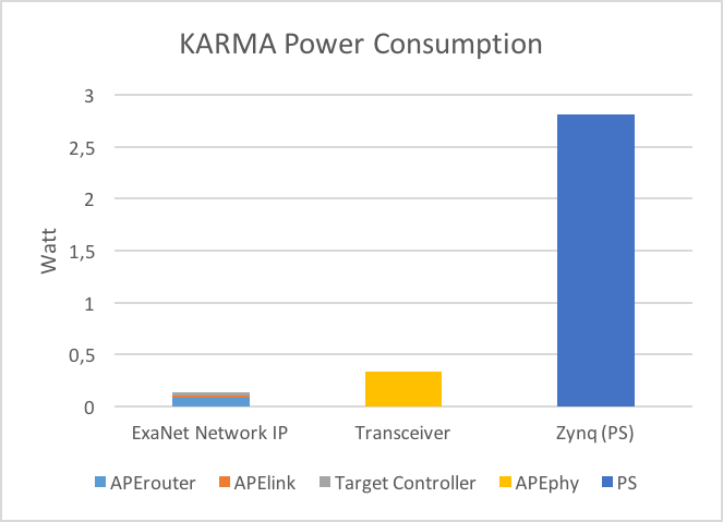
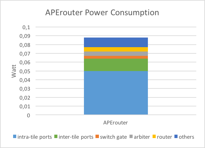
The total APErouter power consumption is 0.088 W, whereas 72% is the fraction taken by the inter- and intra-tile ports. Thus, the size of the FIFOs and the number of implemented virtual channels modify the final result. Although a fine tuning should reduce the values, the achieved result is encouraging nonetheless. The power consumption for each APElink TCL is negligible (0.009 W) while the Aurora transceivers of the APEphy consumes 0.337 W. The amount of channel provided by the I/O interface is indeed the main factor. Finally, the Zynq Ultrascale+ drains 2.822 W, thus the total power consumption of each board of the development platform is 3.5 W.
4.2 Latency test
The measurements of the round-trip latencies between two boards — shown in Figure 8 and Figure 8 — were taken bypassing the kernel driver to avoid the notoriously non-optimal bounce-buffering mechanism and the slow interrupt handling by GNU/Linux. This was done implementing a user-space ping-pong application which exploits /dev/mem to directly access the memory-mapped hardware.
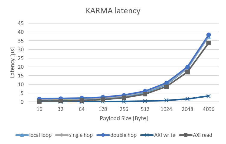
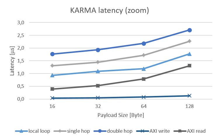
The stated difference in time of s for the two- and one-hop measurements provides an estimate of the single-hop traversal time contribution to the total latency. The times spent by the ARM in reading (s, about 20 clock cycles per word) and in writing (s, 4 clock cycles per word) on the intra-tile port are independent from the number of hops.
4.3 Hardware Bandwidth Test
As stated before, the KARMA testbed was not designed with the purpose of evaluating the bandwidth of the device under test. Nevertheless, the FPGA firmware provides a self-test mechanism to measure the bandwidth of the ExaNet Network IP.
The self-test mechanism is composed by three simple IPs: (i) the Traffic Generator generates EXApackets and fills in the transmitting FIFOs; (ii) the Consumer flushes the receiving FIFOs avoiding the overflow; (iii) the Performance Counter samples and stores the clock cycles needed to complete the data transfers. Configuration registers can customize these self-test packets in their type, size, destination coordinates and ports.
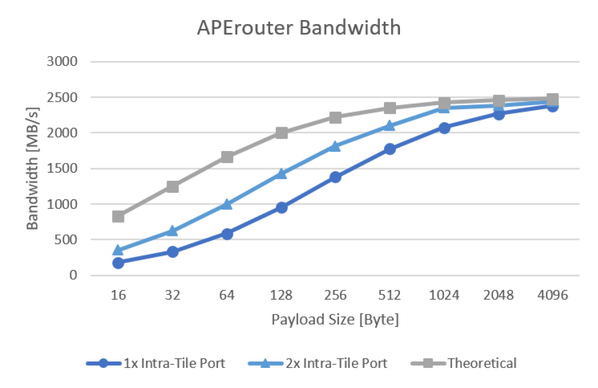
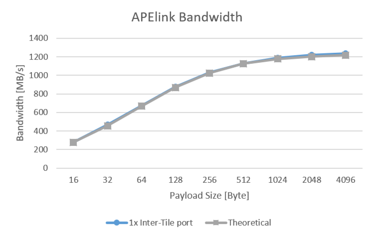
Figure 10 shows the bandwidth achieved by the APErouter when moving data between two ports. The square markers denote the theoretical peak bandwidth considering the 128-bit bus operating at 156.25 MHz. The efficiency is for a 512-byte packet — i.e. the maximum packet size — when the protocol overhead is . The performance loss is due to the unoptimized pipeline of the APErouter hardware IP. Some improvements are gained doubling the sending ports (i.e. Intra-Tile ports) and transmitting packets to the same target port; in this case, the efficiency at 512 byte is .
The APElink result is shown in Figure 10. The theoretical bandwidth is capped at 10 Gbps due to the SFP+ connectors of the Trenz Boards. The efficiency is for 512-byte packets, which is aligned with the estimate.
4.4 Conclusion
In this paper we introduced ExaNet: a modular, low latency, high throughput network architecture suitable for next generation HPC systems under design in ExaNeSt and EuroExa H2020 projects. The preliminary results are very encouraging, taking into account the available margins we have for optimization and improvement: i) a sub- single-hop, node-to-node roundtrip packet transfer latency and ii) a measured bandwidth close to the peak limit for small-to-medium size packets.
The next step foresees the improvement of the current ExaNet IP to be integrated in the ExaNeSt final prototype. The design will focus on adding more inter-node APElink channels and intra-tile ports to implement and test ExaNeSt direct network topologies and sustain the QFDB generated traffic. The ExaNet architecture will be enriched by the addition of new IP blocks in order to accelerate collective operations and support adaptive routing to improve network performances and fault tolerance. In the course of 2018, the ExaNet IP will be deployed in the ExaNeSt final prototype and ported on the coming EuroExa testbeds.
Acknowledgment
This work has received funding from the European Union’s Horizon 2020 Research and Innovation Programme under No. 671553 (ExaNeSt) and Grant Agreement No. 720270 (HBP SGA1).
References
- [1] Rajovic N et al. 2016 The mont-blanc prototype: An alternative approach for hpc systems SC16: International Conference for High Performance Computing, Networking, Storage and Analysis pp 444–455
- [2] Marazakis M et al. 2016 Euroserver: Share-anything scale-out micro-server design 2016 Design, Automation Test in Europe Conference Exhibition (DATE) pp 678–683
- [3] Katevenis M et al. 2016 The ExaNeSt Project: Interconnects, Storage, and Packaging for Exascale Systems 2016 Euromicro Conference on Digital System Design (DSD) pp 60–67
- [4] ExaNoDe accessed: 2017-02-02 URL http://exanode.eu/
- [5] Mavroidis I et al. 2016 Ecoscale: Reconfigurable computing and runtime system for future exascale systems 2016 Design, Automation Test in Europe Conference Exhibition (DATE) pp 696–701
- [6] Xilinx Zynq Ultrascale+ MPSoC devices accessed: 30/Oct/2017 URL https://www.xilinx.com/products/silicon-devices/soc/zynq-ultrascale-mpsoc.html
- [7] Euroexa website accessed: 30/Oct/2017 URL http://cordis.europa.eu/project/rcn/210095_en.html
- [8] Ammendola R et al. 2011 Journal of Physics: Conference Series 331 052029
- [9] Trenz systems website accessed: 30/Oct/2017 URL https://www.trenz-electronic.de/en/
- [10] Ammendola R et al. 2011 QUonG: A GPU-based HPC system dedicated to LQCD computing Application Accelerators in High-Performance Computing (SAAHPC), 2011 Symposium on pp 113–122
- [11] Kermani P and Kleinrock L 1979 Computer Networks 3 267–286
- [12] Ammendola R et al. 2015 Future Generation Computer Systems 53 90 – 99 ISSN 0167-739X URL http://www.sciencedirect.com/science/article/pii/S0167739X14002751