Effective g factor of 2D holes in strained Ge quantum wells
Abstract
The effective g-factor of 2D holes in modulation doped p-SiGe/Ge/SiGe structures was studied. The AC conductivity of samples with hole densities from to was measured in perpendicular magnetic fields up to using a contactless acoustic method. From the analysis of the temperature dependence of conductivity oscillations, the -factor of each sample was determined. The -factor was found to be decreasing approximately linearly with hole density. This effect is attributed to non-parabolicity of the valence band.
I Introduction
Over the last few years, modulation doped SiGe/Ge/SiGe structures with a 2D hole gas have constantly been a subject of interest, due to their high hole mobilities and epitaxial compatibility with Si. Recently, homogenous samples with hole mobility high enough to observe the integer and even the fractional quantum Hall effect have become available.Shi et al. (2015); Mironov et al. (2016)
In such structures the lattice constant mismatch between SiGe and Ge leads to compressive strain in the Ge quantum well. This strain lifts the degeneracy of the heavy hole and light hole subbands in the -point. In the relevant case of compressive strain, the heavy hole subband lies higher in energy, which gives the opportunity to investigate the properties of only heavy holes. The subbands, interact with each other, however, and this interaction gives rise to valence band non-parabolicity. It can manifest itself through hole density dependencies of effective mass and g-factor. The former has been studied extensively.Irisawa et al. (2003); Rössner et al. (2007)
Because of the large g-factor of bulk Ge (), the -factor of 2D holes in Ge quantum wells is also expected to be large and to depend on the hole density due to valence band non-parabolicity. However, until very recently, only a few values of the -factor in SiGe/Ge/SiGe structures have been present in literature.Shi et al. (2015); Arapov et al. (2004, 2007); Nenashev et al. (2003) The first investigation of the -factor dependence on hole density was published in 2017.Lu et al. (2017) Its authors studied the the -factor of 2D holes in a heterostructure field-effect transistor with low hole densities from to . The aim of the present work is to continue the investigation of the -factor in the region of higher hole densities.
II Experimental results and discussion
II.1 Samples
We have studied modulation-doped single p-SixGe1-x/Ge/SixGe1-x quantum wells with hole densities from to . They had all been grown on Si(001) substrates using low-energy plasma-enhanced chemical vapor deposition (LEPECVD).Isella et al. (2004) Symmetrically and asymmetrically doped samples have both been studied. A summary of the samples is presented in Table 1.
| Sample | Hole density | QW width | Doping layers | |
|---|---|---|---|---|
| () | (nm) | |||
| 7989-2 | 13 | 0.3 | at each side | |
| 6745-3 | 15 | 0.3 | single-sided | |
| 8005 | 13 | 0.3 | at each side | |
| 6745-2 | 15 | 0.3 | single-sided | |
| 6777-2 | 15 | 0.3 | single-sided | |
| K6016 | 20 | 0.4 | single-sided | |
| 7974-2 | 13 | 0.3 | at each side |
II.2 Method
We used the contactless acoustic methodWixforth et al. (1986); Drichko et al. (2009) to determine the complex AC conductance of the 2D hole gas, . In the present work, however, we were generally focused on the real part, , of the complex conductance.
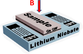
A schematic of the experiment setup is shown in Fig. 1. The samples are mounted onto a LiNbO3 piezoelectric crystal with a pair of interdigital transducers (IDT), which induce a surface acoustic wave (SAW) on the crystal surface. A SAW-induced AC electric field penetrates the sample and interacts with charge carriers (holes). As a result, the SAW attenuation and velocity both acquire additional contributions, which can be related to the complex conductance with the following formulaeKagan (1997):
| (1) | ||||
where is the electromechanical coupling constant for LiNbO3; and are the SAW wave vector and velocity in LiNbO3, respectively; is the vacuum gap between the LiNbO3 crystal and the sample; is the distance between the sample surface and the QW layer; , and are the dielectric constants of LiNbO3, of vacuum, and of the semiconductor, respectively; and – are complex functions of , , , , , and .

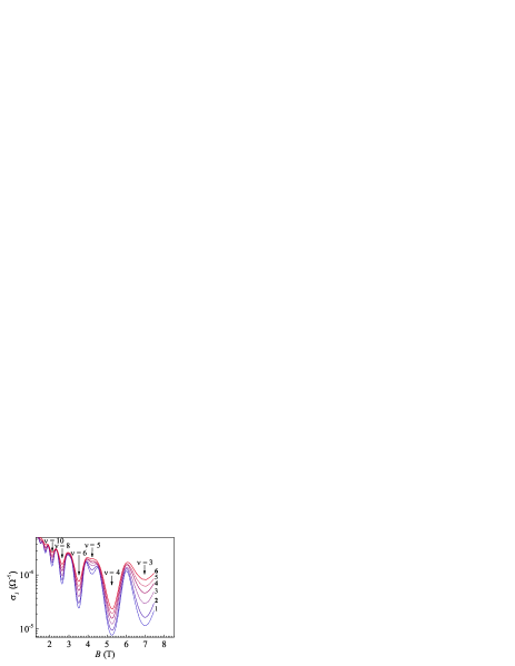
Measurements of the SAW attenuation and velocity have been performed in magnetic fields up to perpendicular to the QW plane and at temperatures from 1.7 to . Fig. 2 shows and plotted as functions of magnetic field. Both curves demonstrate oscillations. The real part of the complex conductance was then obtained from these measurements by solving equations (1). Fig. 3 shows the conductance of sample 6777-2 calculated in this way, as a function of magnetic field at different temperatures. The curves demonstrate Shubnikov – de Haas oscillations, which evolve into the characteristic oscillations of the integer quantum Hall effect regime in stronger fields. The same picture has been observed with all samples.
II.3 Determination of g-factor
The analysis of the temperature dependence of the conductance at the minima of the oscillations allows us to determine the -factor using the following procedure. We have found that at each oscillation minimum there is a temperature range where the conductance is characterized by a constant activation energy :
| (2) |
We have then determined for each minimum by performing linear fitting of the dependence of on .
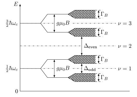
On the other hand, one can write down expressions for activation energy considering the Landau level structure at the minima of oscillations, where the Fermi level is halfway between adjacent Landau levels. Even and odd filling factors correspond to orbital and spin splitting of Landau levels, respectively, as is shown in Fig. 4. Taking the Landau level broadening into account as (Ref. Coleridge, 2003), one can express activation energies for even and odd filling factors as
| (3) | ||||
| (4) |
where is the cyclotron energy, and is the Bohr magneton. Equations (3) and (4) are then solved for and for each pair.
| () | |||
|---|---|---|---|
| 3 | 6 | 8.5 | 0.8 |
| 3 | 8 | 8.5 | 0.8 |
| 3 | 10 | 8.3 | 0.8 |
| 3 | 12 | 8.4 | 0.8 |
| 5 | 6 | 8.4 | 0.8 |
| 5 | 8 | 8.4 | 0.8 |
| 5 | 10 | 8.2 | 0.8 |
| 5 | 12 | 8.2 | 0.8 |
| Sample | Hole density () | -factor |
|---|---|---|
| 7989-2 | ||
| 6745-3 | ||
| 8005 | ||
| 6745-2 | ||
| 6777-2 | ||
| K6016 | ||
| 7974-2 |
Table 2 shows the values obtained for sample 6777-2. On can see from the table that the -factor does not depend on the magnetic field within our experimental error (estimated as –).
Using the procedure described above, we have obtained the values of -factor for every sample; the results are listed in Table 3. It is worth mentioning that the effective mass dependence on the hole density has been neglected in our calculations, and a constant value of , where is the free electron mass, has been taken instead. This approximation is valid because the effective mass changes only by within the range of carrier densities studied in the present work.Rössner et al. (2007)
II.4 Discussion
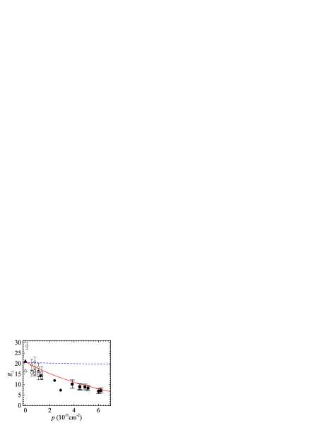
Fig. 5 summarizes the results of several studies of the -factor value in SiGe/Ge/SiGe structures, including those of the present work. We attribute the decrease in the -factor to valence band non-parabolicity, which is due to the mixing of HH and LH states away from the zone center. At the center of the valence band the -factor of 2D holes should be approximately equal to the g-factor of heavy holes in bulk Ge (). With growing hole density, the -factor is expected to decrease from the band-center value.
The reason is that in the presence of non-zero momentum component along the QW plane, the hole state is no longer the pure heavy hole state but contains an admixture of the light hole state . The degree of this admixture is roughly proportional to , which, at the Fermi level, is proportional to the hole density. Thus, the -factor becomes a combination of the -factors of heavy and light holes, taken with weights which are proportional to fractions of heavy and light holes in the observed state.Nenashev The result of a calculationNenashev based on the Hamiltonian in the infinite well approximation is shown with the blue dashed line in Fig. 5. As is seen from the figure, this theoretical curve fails to describe the experimental results.
Several numerical calculations that were based on a more rigorous model with the Hamiltonian have been made to explain the density dependence of the effective mass.Rössner et al. (2007); Winkler et al. (1996) In these works, along with the split-off (SO) band, self-consistent potential profiles and the effects of strain due to the lattice mismatch between Ge and SiGe were also taken into account. The results of these computations show good agreement with the experimental dependence of the effective mass on density. The structures studied in Ref. Rössner et al., 2007 have almost the same parameters as those investigated in the present work, so we used the results of calculations from Ref. Rössner et al., 2007 to interpret the -factor dependence on density as follows.
As the density dependencies of both effective mass and -factor of heavy holes have the same microscopic nature, they can be related to each other as followsWimbauer et al. (1994):
| (5) |
where is the free electron mass, , and are the Luttinger parameters of Ge. Ivchenko and Pikus (2012) The dependence of the -factor on density was evaluated from the theoretical dependence of the effective mass on densityRössner et al. (2007) by means of formula (5). The result is shown with the solid line in Fig. 5. As is seen, it describes the experimental data with good agreement. Thus, the observed experimental -factor dependence on density can be attributed to the interaction between HH, LH and SO subbands, as affected by the strain present in the quantum well.
III Conclusions
We have performed contactless conductance measurements on the 2D hole gas in p-SiGe/Ge/SiGe structures by means of acoustic spectroscopy, and determined the effective -factor. It was found that the -factor depends approximately linearly on the hole density, but is independent of the magnetic field, the Si content in the spacer layers, and the character of the modulation doping (see Table 1). The observed change is attributed to valence band non-parabolicity.
Acknowledgements.
We are grateful to A. V. Nenashev, S. A. Tarasenko, M. V. Durnev, and N. G. Shelushinina for useful discussions of the experimental results. Author A. A. D. also acknowledges the support by the Government of the Russian Federation (Grant 074-U01).References
- Shi et al. (2015) Q. Shi, M. A. Zudov, C. Morrison, and M. Myronov, Phys. Rev. B 91, 241303 (2015).
- Mironov et al. (2016) O. A. Mironov, N. d’Ambrumenil, A. Dobbie, D. R. Leadley, A. V. Suslov, and E. Green, Phys. Rev. Lett. 116, 176802 (2016).
- Irisawa et al. (2003) T. Irisawa, M. Myronov, O. A. Mironov, E. H. C. Parker, K. Nakagawa, M. Murata, S. Koh, and Y. Shiraki, Appl. Phys. Lett. 82, 1425 (2003), https://doi.org/10.1063/1.1558895 .
- Rössner et al. (2007) B. Rössner, H. von Känel, D. Chrastina, G. Isella, and B. Batlogg, Semicond. Sci. Technol. 22, S191 (2007).
- Arapov et al. (2004) Y. G. Arapov, G. I. Harus, N. G. Shelushinina, M. V. Yakunin, V. N. Neverov, O. A. Kuznetsov, L. Ponomarenko, and A. De Visser, Sov. J. Low Temp. Phys. 30, 867 (2004), https://doi.org/10.1063/1.1819865 .
- Arapov et al. (2007) Y. G. Arapov, S. V. Gudina, I. V. Karskanov, V. N. Neverov, G. I. Harus, and N. G. Shelushinina, Sov. J. Low Temp. Phys. 33, 160 (2007), https://doi.org/10.1063/1.2409654 .
- Nenashev et al. (2003) A. V. Nenashev, A. V. Dvurechenskii, and A. F. Zinovieva, Phys. Rev. B 67, 205301 (2003).
- Lu et al. (2017) T. M. Lu, C. T. Harris, S.-H. Huang, Y. Chuang, J.-Y. Li, and C. W. Liu, Appl. Phys. Lett. 111, 102108 (2017), https://doi.org/10.1063/1.4990569 .
- Isella et al. (2004) G. Isella, D. Chrastina, B. Rössner, T. Hackbarth, H.-J. Herzog, U. König, and H. von Känel, Solid-State Electron. 48, 1317 (2004).
- Wixforth et al. (1986) A. Wixforth, J. P. Kotthaus, and G. Weimann, Phys. Rev. Lett. 56, 2104 (1986).
- Drichko et al. (2009) I. L. Drichko, A. M. Diakonov, E. V. Lebedeva, I. Y. Smirnov, O. A. Mironov, M. Kummer, and H. von Känel, J. Appl. Phys. 106, 094305 (2009), https://doi.org/10.1063/1.3251568 .
- Kagan (1997) V. D. Kagan, Sov. Phys. Semicond. 31, 407 (1997).
- Coleridge (2003) P. T. Coleridge, Solid State Commun. 127, 777 (2003), advances in Studies of Electrons in Low Dimensional Structures.
- (14) A. V. Nenashev, private communications.
- Winkler et al. (1996) R. Winkler, M. Merkler, T. Darnhofer, and U. Rössler, Phys. Rev. B 53, 10858 (1996).
- Wimbauer et al. (1994) T. Wimbauer, K. Oettinger, A. L. Efros, B. K. Meyer, and H. Brugger, Phys. Rev. B 50, 8889 (1994).
- Ivchenko and Pikus (2012) E. L. Ivchenko and G. Pikus, Superlattices and other heterostructures: symmetry and optical phenomena, Vol. 110 (Springer Science & Business Media, 2012).