Phosphorus oxide gate dielectric for black phosphorus field effect transistors
Abstract
The environmental stability of the layered semiconductor black phosphorus (bP) remains a challenge. Passivation of the bP surface with phosphorus oxide, POx, grown by a reactive ion etch with oxygen plasma is known to improve photoluminescence efficiency of exfoliated bP flakes. We apply phosphorus oxide passivation in the fabrication of bP field effect transistors using a gate stack consisting of a POx layer grown by reactive ion etching followed by atomic layer deposition of Al2O3. We observe room temperature top-gate mobilities of 115 cm2V-1s-1 in ambient conditions, which we attribute to the low defect density of the bP/POx interface.
Black phosphorus (bP) is a direct band gap () semiconductor with a puckered honeycomb layer structure characterized by van der Waals interlayer bonding morita1986semiconducting ; keyes1953electrical . The most thermodynamically stable allotrope of phosphorus, bP exhibits ambipolar conduction, anisotropic conductivity, and can be exfoliated down to the atomic monolayer limit li2014black ; xia2014rediscovering ; liu2014phosphorene ; tayari2015two . Exfoliation of bP in a nitrogen environment followed by encapsulation with hexagonal boron nitride in a vacuum environment has led to the observation of hole mobility at cryogenic temperatures long . Importantly, bP is subject to degradation by photo-oxidation with a reaction rate that increases as bP thickness decreases favron2015photooxidation . A number of passivation techniques have been developed with varying degrees of success, including encapsulation with Al2O3 na2014few ; wells2015passivation ; kim2014toward ; das2014ambipolar , hexagonal boron nitride (h-BN) chen2015high ; cao2015quality ; avsar2015air ; long , polymer layers tayari2015two ; passaglia and functionalization with nickel nanoparticles caporali . More recently, it has been demonstrated that the formation of a dense phosphorus oxide, POx, layer by oxygen plasma dry etching followed by Al2O3 deposition results in stable encapsulation of bP without compromising photoluminescence (PL) efficiency pei2016producing . The preservation of PL efficiency indicates that the interface between bP and POx does not measurably increase non-radiative recombination rates and is thus an effective surface passivation strategy.
In this work, we apply the POx passivation approach of Pei et al.pei2016producing to fabricate top-gated bP field effect transistors (FETs). The use of a native oxide for passivation and gate stack formation in bP FETs is appealing as a direct analogue to the use of silicon oxide in silicon FET technology. Various phases of POx are known, including a rhombohedral crystal of molecular P4O10 cruickshank1 , and the most thermodynamically stable form of P2O5 which is itself a layered material composed of a hexagonal network of edge connected tetrahedra stachel . The POx layer passivates the bP surface, and acts as a seeding layer for subsequent atomic layer deposition of high-quality gate dielectrics such as Al2O3. We have fabricated dual-gate bP FETs, a bottom gate formed by a heavily doped, oxidized silicon substrate, and a top gate structure with a POx/Al2O3 dielectric stack. Room temperature top gate field effect mobilities of up to are achieved.
In our experiments, we used bP crystals prepared according to the procedure developed by Nilges et al. nilges2008fast , wherein high-purity red phosphorus ( 99.99%), tin ( 99.999%), and gold ( 99.99%) are heated in a muffle oven with a SnI4 catalyst. The solid product was placed in a quartz tube, subjected to several evacuation-purge cycles with N2 gas, and then sealed under vacuum. The evacuated quartz tube was heated to 406∘C at 4.2∘C/min, where it remained for 2 hours. The tube was then heated to 650∘C at 2.2∘C/min and held at this temperature for 3 days. The tube was then cooled at 0.1∘C/min. The final product is crystalline bP with a typical crystal size ranging from 0.3 mm 3 mm to 3 mm 10 mm. The bP crystals were mechanically exfoliated in a nitrogen glove box with H2O and O2 levels maintained at to minimize photo-oxidation during sample processing. The bP flakes were exfoliated onto either single crystal quartz substrates, or As-doped, (001) Si substrates with 300 nm of dry thermal SiO2. The SiO2 surface was treated with a hexamethyldisilazane (HMDS) layer to suppress charge transfer doping lafkioti .
Amorphous POx was grown on both bulk bP crystals and exfoliated bP flakes by reactive ion etching (RIE) in a custom built chamber with 10 sccm of O2 flow at a chamber pressure of 200 mTorr with 300 W of RF bias power. Prior to oxidizing the bP samples, the RIE chamber was cleaned for 15 min with 10 sccm of O2, 200 mTorr pressure and 300 W RF power. As discussed further below, the RIE process simultaneously oxidizes and etches the bP. We calibrated the RIE process by etching thick exfoliated flakes as shown in Fig. 1 a)-c). Stylus profilometer traces were taken before and after RIE processing, with the results of a 17 min etch shown in Fig. 1 b) and c). The estimated etch rate for our process is 0.98 Å/s, which corresponds to an etch rate of 0.18 layers/s taking into account the 5.23 Å thickness per layer morita1986semiconducting . By comparison, Pei et al. report a comparable etch rate of 0.1 layers/s pei2016producing . In our work, typical RIE processing times for thin () exfoliated bP flakes are 1-3 minutes, allowing for the growth of POx with minimal etching.
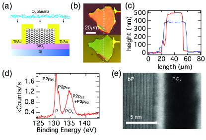
To confirm the formation of POx, a freshly cleaved bP crystal was treated by RIE and analyzed by X-ray photoemission spectroscopy (XPS) with an Al Kα source. The resulting XPS spectrum of the P core level is shown in Fig.1(d), showing contributions from both bP and POx. The P peak at a binding energy of 130 eV and spin-orbit split P peak are in good agreement with previous observations of bP XPS spectrapei2016producing ; edmonds2015creating . The overlapping P and P peaks at a binding energy of 134.5 eV are in remarkably good agreement with previous reports for P2O5 pei2016producing ; edmonds2015creating ; sherwood . However, it remains a challenge to distinguish between the various phases of POx gaskell .
The oxidation process is best understood by the model described by Pei et al. pei2016producing . In the RIE process, O2 plasma oxidizes the top layers of the bP, producing a dense POx layer. Once this layer is established, subsequent etching by O2 plasma penetrates the underlying bP, leading to further oxidation and POx formation, while simultaneously sputtering away POx. A dynamic equilibrium is established between the sputtering of POx and oxidation of the underlying bP, such that the POx layer reaches a steady-state thickness. Pei et al. pei2016producing estimates a steady state thickness of approximately 10 nm after 40 s of oxidation, approximately twice the 5 nm thickness observed in our experiments (see below).
Notably, POx is a strong hygroscopic desiccant and reacts violently with water. In order to suppress the reaction of POx with water, we encapsulated the bP/POx flakes with a 3 nm thick layer of Al2O3 by atomic layer deposition, exposing them to trimethylaluminum (TMA) for 148 seconds before proceeding with 25 ALD deposition cycles. By increasing exposure to hygroscopic TMA, the bP/POx surface is in a dehydrated state before the introduction of H2O into the ALD chamber to initiate oxidation of adsorbed TMA.
Transmission electron microscopy (TEM), was used to characterize the bP/POx/Al2O3 and bP/SiO2 interfaces. An exfoliated bP sample was capped with a POx layer grown for 3 min by RIE followed by a 3 nm layer of Al2O3 grown by ALD. A tungsten layer was deposited atop the flake for protection during the milling and polishing process. Electron energy loss spectroscopy (EELS) confirmed the presence of P, Al, and O. Fig. 1(e) displays a high-angle annular dark-field (HAADF) image of the surface of the bP flake. The puckered honeycomb layers of P atoms in the bP crystal are clearly seen, as well as an amorphous layer of POx. We speculate that the POx is an amorphous layer of molecular P4O10, but further work is required for unambiguous determination of the POx phase. The POx layer thickness is approximately .
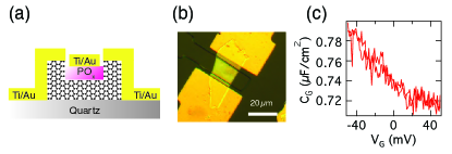
We measured the capacitance of the POx layer alone as a gate dielectric with bP flakes fabricated on an insulating quartz substrate. A schematic of the bP device is displayed in Fig. 2(a). The bP flakes were first exfoliated on a quartz substrate and contacted with Ti/Au (5 nm / 80 nm) electrodes using an electron beam lithography process. The POx was then deposited by 3 min of RIE. Finally, a second electron beam lithography process was used to deposit Ti/Au (5 nm / 80 nm) gate electrodes. An optical micrograph of a device before top-gate metallization is shown in Fig. 2(b). The top-gate capacitance per unit area versus top-gate dc bias voltage was measured with an AC excitation of peak-to-peak at a frequency of 1.00 MHz, and is displayed in Fig. 2(c). At , the capacitance per unit area is . The gate capacitance is a series combination of: the capacitance of the POx layer; and the gate voltage dependent quantum capacitance of the hole accumulation layer at the bP surface. The latter capacitance contribution is approximated from a non-degenerate thermodynamic density of states as for an estimated carrier density at . Consequently, we find the POx layer contribution . For an estimated POx layer thickness of nm determined from TEM images, the inferred dielectric constant of our POx layer is .
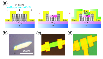
We fabricated devices for field effect measurements in a dual gate configuration, similar to that first proposed by Sakaki for velocity modulated transistors sakaki1982velocity , and recently used to compare top-gate and back-gate operation in bP FETs tayari2016dual . A schematic of the fabrication process is shown in Fig. 3(a). A freshly exfoliated bP flake on an SiO2/Si substrate is displayed in Fig. 3(b). A standard electron beam lithography process was used to define Ti/Au (5 nm / 80 nm) source-drain electrodes (Fig. 3(c)). The POx and Al2O3 layers were then deposited by 3 min of RIE and 25 cycles of ALD. Finally, a second electron beam lithography process was used to define Ti/Au (5 nm / 80 nm) top gate electrodes (Fig. 3(d)). For further protection, bP FETs were encapsulated with polymethylmethacrylic (PMMA) layers. Taking into account the capacitance of the 3 nm layer of Al2O3, the top-gate capacitance is estimated to be . The back-gate capacitance is a significantly smaller .
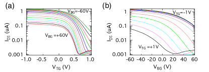
All electrical measurements were carried out in a vacuum probe station, using quasi-dc excitation with a semiconductor parameter analyzer. Leakage currents through the top and bottom oxide layers were measured through-out all measurements, and never exceeded 5% of the measured source-drain current for all results shown here. Fig. 4 a) and b) display the characteristics of our highest-mobility POx/Al2O3-passivated device. The source-drain current versus bottom-gate voltage with fixed top-gate voltage at a source-drain bias voltage at a temperature of 300 K is plotted in Fig. 4(a). Similarly, versus top-gate voltage with fixed bottom-gate voltage at a source-drain bias voltage is shown in Fig. 4(b). In both cases, hole conduction is observed, with an on/off current ratio for the bottom-gate and top-gate modulation of and , respectively. Noting that the capacitance ratio , the top-gate voltage range and bottom-gate voltage range extend over an induced charge displacement of approximately .
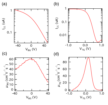
The field effect mobility is determined from the channel conductance by , where is the channel length, is the channel width and refers to either top-gate (TG) or bottom-gate (BG). The room temperature field effect mobilities are plotted in Fig. 4(c) and Fig. 4(d). The peak top-gate mobility of exceeds the peak back-gate mobility of in the same bP FET. The POx/Al2O3 top-gate is thus seen to give 10-fold improvement in on/off current ratio and a 50% improvement in peak field effect mobility over the SiO2 back-gate. In the case of both top-gate and back-gate modulation seen in Fig. 4(c) and (d), the field effect mobility falls to a negligible value at positive bias due to the depletion of hole density and subsequent loss of conductance modulation. At negative bias, channel conductance saturates due to the parasitic effects of access resistance and contact resistance, suppressing transconductance and leading to an under-estimation of field effect mobility. The saturation of conduction at negative bias is more prevalent with top-gate modulation than bottom-gate modulation because the top gate modulates a smaller area of the channel than the bottom gate, and thus the top-gate configuration suffers from higher access resistance. Despite the difference in access resistance, the field effect mobility extracted from raw conductance modulation data is superior in the top-gate configuration.
There are a number of physical mechanisms that may lead to an improvement in transfer characteristics in a top-gated hole accumulation layer: a reduced density of charged impurities at the top bP/POx interface as compared to the bP/SiO2 interface, stronger screening of charged impurities due to the shorter electrical length of the top-gate versus the bottom-gate, and a reduced contact and access resistance to the top accumulation layer where the source-drain electrodes are deposited as compared with the bottom accumulation layer. More subtle mechanisms, such as the role of phonon scattering at the respective bP/dielectric interfaces could also play a role.
Lastly, we investigated bp FET channel modulation in a dual-gate mode, akin to the velocity modulated transistor proposed by Sakaki sakaki1982velocity . The source-drain current versus top-gate voltage at a variety of bottom-gate voltages is plotted in Fig. 5(a). Similarly, versus bottom-gate voltage at a variety of top-gate voltages is plotted in Fig. 5(b). Several effects in the dual-gate mode are evident. Both the threshold voltage and on-current for hole accumulation induced by one gate voltage is modulated by the voltage applied to the other gate. The former effect is a consequence of both gate electrodes modulating the potential through-out the exfoliated bP flake. The latter effect is a consequence of gate modulation of both contact resistance and channel mobility, as has been previously observed in bP tayari2016dual . Notably, the peak top-gate field effect mobility can be increased to at a bottom-gate voltage .
The improvement in mobility of a hole accumulation layer at the bP/POx interface in this work as compared to the bP/Al2O3 interface of previous worktayari2016dual can be attributed to the combined action of etching away the bP surface damaged by oxidation under ambient conditions and the low defect density of the bP/POx interface formed by RIE pei2016producing . The RIE process etches away the bP surface exposed to ambient water and oxygen favron2015photooxidation , allowing a clean bP/POx interface to be formed. The POx layer formed by RIE is itself an ideal seeding layer for subsequent ALD steps to enable gate dielectric engineering. In contrast, ALD of a top-gate dielectric such as Al2O3 directly atop bP is subject to the low quality of an ambient exposed bP surface.
In summary, we have shown that the POx/Al2O3 layers produced by RIE and ALD treatment of bP can be used as an effective gate dielectric stack in bP FETs with on/off current ratios and field effect mobilities of at room temperature, exceeding the performance on the SiO2 bottom-gate in the same bP FET channel. The simple POx/Al2O3 process enables the fabrication of dual-gated FETs, which have seen great interest in the context of the Stark effect, where band structure is modulated by applied electric field Deng2017 ; Yan2017 .
Acknowledgements W.D., V.T., I.F. and T.S. acknowledge support from the Canadian Natural Sciences and Engineering Research Council, Fonds Québecois de Recherche - Nature et Technologies. The TEM work (HAADF imaging and EELS) was carried out at the Canadian Centre for Electron Microscopy, a facility supported by the Canada Foundation for Innovation under the MSI program, NSERC and McMaster University. M.C., M.S.-R., S.H. and M.P. express thanks to the European Research Council for funding the project PHOSFUN Phosphorene functionalization: a new platform for advanced multifunctional materials (Grant Agreement No. 670173) through an ERC Advanced Grant to MP. S.H. acknowledges support from Scuola Normale Superiore, project SNS16 B HEUN-004155.
References
- (1) A. Morita, Semiconducting black phosphorus, Applied Physics A: Solids and Surfaces, 39, 227 (1986).
- (2) R. W. Keyes, The electrical properties of black phosphorus, Physical Review, 92, 3 (1953).
- (3) L. Li, Y. Yu, G. J. Ye, Q. Ge, X. Ou, H. Wu, D. Feng, X. H. Chen, and Y. Zhang, Black phosphorus field-effect transistors, Nature Nanotechnology, 9, 5 (2014).
- (4) F. Xia, H. Wang, and Y. Jia, Rediscovering black phosphorus as an anisotropic layered material for optoelectronics and electronics, Nature Communications, 5, 4458 (2014).
- (5) H. Liu, A. T. Neal, Z. Zhu, X. Xu, D. Tomanek, P. D. Ye, and Z. Luo, Phosphorene: an unexplored 2D semiconductor with a high hole mobility, ACS Nano, 8, 4 (2014).
- (6) V. Tayari, N. Hemsworth, I. Fakih, A. Favron, E. Gaufrès, G. Gervais, R. Martel, and T. Szkopek, Two-dimensional magnetotransport in a black phosphorus naked quantum well, Nature Communications, 6, 7702 (2015).
- (7) G. Long, D. Maryenko, J. Shen, S. Xu, J. Hou, Z. Wu, W. K. Wong, T. Han, J. Lin, Y. Cai, R. Lortz, and N. Wang, Achieving Ultrahigh Carrier Mobility in Two-Dimensional Hole Gas of Black Phosphorus, Nano Lett. 16, 7768 (2016).
- (8) E. Passaglia, F. Cicogna, G. Lorenzetti, S. Legnaioli, M. Caporali, M. Serrano-Ruiz, A. Ienco, and M. Peruzzini, Novel polystyrene-based nanocomposites by phosphorene dispersion, RSC Advances 6, 53777 (2016).
- (9) A. Favron, E. Gaufrès, F. Fossard, A.-L. Phaneuf-LHeureux, N. Y. Tang, P. L. Lévesque, A. Loiseau, R. Leonelli, S. Francoeur, and R. Martel, Photooxidation and quantum confinement effects in exfoliated black phosphorus, Nature Materials, 14, 8 (2015).
- (10) J. Na, Y. T. Lee, J. A. Lim, D. K. Hwang, G.-T. Kim, W. K. Choi, and Y.-W. Song, Few-layer black phosphorus field-effect transistors with reduced current fluctuation, ACS Nano, 8, 11 (2014).
- (11) S. Wells, J. Wood, D. Jariwala, K.-S. Chen, E. Cho, V. Sangwan, X. Liu, L. Lauhon, T. Marks, and M. Hersam, Passivation of exfoliated black phosphorus transistors against ambient degradation, in APS March Meeting Abstracts, 1, (2015).
- (12) J.-S. Kim, Y. Liu, W. Zhu, S. Kim, D. Wu, L. Tao, A. Dodabalapur, K. Lai, and D. Akinwande, Toward air-stable multilayer phosphorene thin-films and transistors, Scientific Reports, 5, (2015).
- (13) S. Das, M. Demarteau, and A. Roelofs, Ambipolar phosphorene field effect transistor, ACS Nano, 8, 11 (2014).
- (14) X. Chen, Y. Wu, Z. Wu, Y. Han, S. Xu, L. Wang, W. Ye, T. Han, Y. He, Y. Cai, et al., High-quality sandwiched black phosphorus heterostructure and its quantum oscillations, Nature Communications, 6, 7315 (2015).
- (15) Y. Cao, A. Mishchenko, G. Yu, E. Khestanova, A. Rooney, E. Prestat, A. Kretinin, P. Blake, M. Shalom, C. Woods, et al., Quality heterostructures from two-dimensional crystals unstable in air by their assembly in inert atmosphere, Nano Letters, 15, 8 (2015).
- (16) M. Caporali, M. Serrano-Ruiz, F. Telesio, S. Heun, G. Nicotra, C. Spinella and M. Peruzzini, Decoration of exfoliated black phosphorus with nickel nanoparticles and its application in catalysis, Chem. Comm. 53, 10946 (2017).
- (17) A. Avsar, I. J. Vera-Marun, J. Y. Tan, K. Watanabe, T. Taniguchi, A. H. Castro Neto, and B. Ozyilmaz, Air-stable transport in graphene-contacted, fully encapsulated ultrathin black phosphorus-based field-effect transistors, ACS Nano, 9, 4 (2015).
- (18) J. Pei, X. Gai, J. Yang, X. Wang, Z. Yu, D.-Y. Choi, B. Luther-Davies, and Y. Lu, Producing air-stable monolayers of phosphorene and their defect engineering, Nature Communications, 7, 10450 (2016).
- (19) D. W. J. Cruickshank, Refinements of Structures Containing, Bonds between Si, P, S or Cl and O or N. V. P4010, Acta Cryst. 17, 677, (1964).
- (20) D. Stachel, I. Svoboda and H. Fuess, Phosphorus Pentoxide at 233 K, Acta Cryst. C51, 1049 (1995).
- (21) M. Lafkioti, B. Krauss, T. Lohmann, U. Zschieschang, H. Klauk, K. v. Klitzing and J. H. Smet, Graphene on a Hydrophobic Substrate: Doping Reduction and Hysteresis Suppression under Ambient Conditions, Nano Lett. 10, 1149 (2010).
- (22) V. Tayari, N. Hemsworth, O. Cyr-Choinière, W. Dickerson, G. Gervais, and T. Szkopek, Dual-gate velocity-modulated transistor based on black phosphorus, Phys. Rev. App. 5, 6, (2016).
- (23) H. Sakaki, Velocity-modulation transistor (VMT)-a new field-effect transistor concept, Jap. J. Appl. Phys. 21, 6A (1982).
- (24) M. Edmonds, A. Tadich, A. Carvalho, A. Ziletti, K. ODonnell, S. Koenig, D. Coker, B. Ozyilmaz, A. C. Neto, and M. Fuhrer, Creating a stable oxide at the surface of black phosphorus, ACS Appl. Mat. & Int. 7, 27 (2015).
- (25) Y. Wang and P. M. A. Sherwood, Phosphorus Pentoxide (P2O5) by XPS, J. Vac. Sci. & Tech. A 22, 4 (2004).
- (26) K. J. Gaskell, M. M. Smith and P. M. A. Sherwood, Valence band x-ray photoelectron spectroscopic studies of phosphorus oxides and phosphates, J. Vac. Sci. Technol. A 22, 1331 (2004).
- (27) T. Nilges, M. Kersting, and T. Pfeifer, A fast low-pressure transport route to large black phosphorus single crystals, J. Sol. State Chem. 181, 8 (2008).
- (28) B. Deng, V. Tran, Y. Xie, H. Jiang, C. Li, Q. Guo, X. Wang, H. Tian, S. J. Koester, H. Wang, J. J. Cha, Q. Xia, L. Yang and F. Xia, Efficient electrical control of thin-film black phosphorus bandgap, Nature Communications 8, 14474 (2017).
- (29) S.-H. Yan, Z.-J. Xie, J.-H. Chen, T. Taniguchi and K. Watanabe, Electrically Tunable Energy Bandgap in Dual-Gated Ultra-Thin Black Phosphorus Field Effect Transistors, Chinese Phys. Lett. 34, 047304 (2017).