Coupling a superconducting quantum circuit to a phononic crystal defect cavity
Abstract
Connecting nanoscale mechanical resonators to microwave quantum circuits opens new avenues for storing, processing, and transmitting quantum information. In this work, we couple a phononic crystal cavity to a tunable superconducting quantum circuit. By fabricating a one-dimensional periodic pattern in a thin film of lithium niobate and introducing a defect in this artificial lattice, we localize a 6 gigahertz acoustic resonance to a wavelength-scale volume of less than one cubic micron. The strong piezoelectricity of lithium niobate efficiently couples the localized vibrations to the electric field of a widely tunable high-impedance Josephson junction array resonator. We measure a direct phonon-photon coupling rate and a mechanical quality factor leading to a cooperativity when the two modes are tuned into resonance. Our work has direct application to engineering hybrid quantum systems for microwave-to-optical conversion as well as emerging architectures for quantum information processing.
I Introduction
Compact and low-loss acoustic wave devices that perform complex signal processing at radio frequencies are ubiquitous in classical communication systems Hashimoto (2015). Much like their classical counterparts, emerging quantum machines operating at microwave frequencies Devoret and Schoelkopf (2013) also stand to benefit from their integration with these devices. This is conditioned on the realization of sufficiently versatile quantum phononic technologies. Several promising approaches have emerged in the last few years. Each has its own strengths and weaknesses and they can be broadly categorized by the degree to which the acoustic waves are confined as compared to their wavelength. In a series of remarkable experiments, thin-film O’Connell et al. (2010), surface Gustafsson et al. (2014); Manenti et al. (2017); Moores et al. (2017); Noguchi et al. (2017), and bulk acoustic wave resonators Chu et al. (2017); Kervinen et al. (2018) made of piezoelectric materials have coupled gigahertz phonons with varying levels of confinement to superconducting circuits. Nonetheless, smaller mode volumes, lower losses, and greater control over the mode structure are desired.
One of the most promising approaches for realizing ultra-low-loss mechanical resonators is to use phononic crystal cavities that confine acoustic waves in all three dimensions. Wavelength-scale confinement and periodicity qualitatively alter the properties of waves and allow far greater control over the phonon density of states. Periodic patterning of a thin slab of elastic material can give rise to a phononic bandgap – a range of frequencies devoid of propagating waves. By introducing defects in such a crystal, mechanical energy is localized at the wavelength scale Eichenfield et al. (2009); Alegre et al. (2010); Bochmann et al. (2013a); Safavi-Naeini et al. (2014); Balram et al. (2015) without any “clamping” losses. The existence of a full phononic bandgap eliminates all modes into which a phonon can be linearly scattered, leading to a significant increase in the coherence time of such resonators. For example, lifetimes on the order of one second corresponding to have been optically measured in GHz phononic crystal cavities made from silicon MacCabe et al. (2018). Moreover, the small mode volume of phononic crystal cavities leads to a dramatic reduction in the density of spurious modes that can negatively impact performance of quantum acoustic systems, while enabling a denser packing of devices for greater scalability.
The greater confinement and control over the acoustic mode structure comes at the cost of weaker coupling. At gigahertz frequencies, the modes of phononic crystal cavities are confined to extremely small volumes (). This leads to smaller forces for a given oscillating voltage when compared to approaches with transducer dimensions of tens to hundreds of microns Arrangoiz-Arriola and Safavi-Naeini (2016). Up to now, it has only been possible to efficiently read out and couple to localized modes of phononic crystal cavities with optical photons where the electromagnetic energy is similarly localized Eichenfield et al. (2009); Liang et al. (2017). Nonetheless, to connect these systems to microwave superconducting quantum circuits, efficient and tunable coupling between microwave photons and phonons is needed. In this work we demonstrate the direct coupling of a superconducting circuit to a wavelength-scale phononic nanocavity, opening a new avenue in quantum acoustics.
II Device design and fabrication
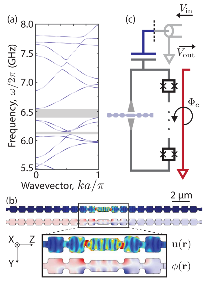
At the heart of our device lies a suspended quasi-one-dimensional phononic crystal fabricated from a 200-nanometer-thick film of lithium niobate (). The crystal has a lattice constant of and has a complete phononic bandgap in the vicinity of [Fig. 1(a)]. This bandgap is used to localize the resonances of a single defect site introduced in the center of the lattice. In particular, we engineer a defect mode with a strain field that generates a charge polarization that is predominantly aligned in-plane in the direction perpendicular to the lattice [Fig. 1(b)]; here is the piezoelectric coupling tensor of . We then use this polarization to couple the defect mode to the microwave-frequency electric field of a readout circuit, applied by gate electrodes placed within nanometers of the defect. The readout circuit is a lumped-element microwave resonator formed from the capacitance of the gate electrodes and a series of Josephson junctions in a superconducting quantum interference device (SQUID) array configuration with total Josephson inductance [Fig. 1(c)], where is the reduced flux quantum. The effective Josephson energy of the array depends on the external flux threading the SQUIDs, making the resonator frequency tunable by applying a small current to an on-chip flux line. In addition, the small parasitic capacitance of the array enables us to achieve a relatively large resonator impedance . This is an important feature of our device, as the piezoelectric coupling strength is proportional to the zero-point voltage fluctuations of the circuit and . The resonator impedance is largely limited by the presence of the flux line (highlighted in red in Fig. 2), which is a major source of parasitic capacitance between the two nodes of the resonator.
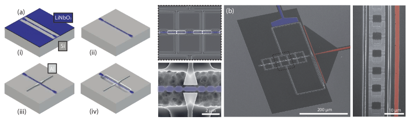
Thin-film has recently gained prominence in the realm of classical radio frequency systems Wang et al. (2013); Pop et al. (2017); Vidal-Álvarez et al. (2017). Here we perform the device fabrication on a film of X-cut on a high-resistivity () Si substrate and involves seven masks of lithography consisting of the following four stages [see Fig. 2(a)]: 1) film thinning, 2) patterning of phononic nanostructures, 3) deposition of Al layers, including all microwave circuitry and Josephson junctions, and 4) masked undercut of structures. The film is first thinned down to the target thickness (approximately 200 nm for this device) by blanket argon milling. We then expose a mask on positive resist with a single step of electron-beam (ebeam) lithography and transfer it to the film with an optimized argon milling process to form the phononic nanostructures. Now masking only the structures, an argon milling step is done to remove the film from the entire sample. This step allows us to place all microwave circuits on a high-resistivity silicon substrate where they are not vulnerable to acoustic radiation losses induced by the piezoelectric film. Aluminum microwave ground planes and feedlines are defined on the exposed silicon via liftoff, and the SQUID arrays are fabricated with a Dolan bridge double-angle evaporation process to grow the Al/AlOx/Al junctions Dolan (1977); Stockklauser et al. (2017). The gate electrodes used to address the phononic defect sites are patterned with a separate ebeam mask and normal-incidence Al evaporation, and finally a bandage process Dunsworth et al. (2017) is used to ensure lossless superconducting connections between all metalization layers. As a final step, we release the structures with a masked dry etch that etches the underlying Si with extremely high selectivity to the and the Al Pop et al. (2017); Vidal-Álvarez et al. (2017), leaving all aluminum layers intact at the end of the process.
In Fig. 2(b) we show a set of scanning-electron micrographs of a finished device nearly identical to the one used in this experiment. The full microwave circuit is shown in the center. The charge line (highlighted blue) is capacitively coupled to the resonator and is used for driving and readout. The flux line (highlighted red) is used to apply either DC or RF magnetic fields to the SQUID array and tune the resonator frequency. The flux line is shorted to ground in a symmetric configuration in order to reduce leakage of photons through the mutual inductance between the resonator and the line. The junction array, placed away from the flux line, is composed of nominally identical SQUIDs in series and has a total inductance inferred by measuring the normal-state resistance of three copies of the array on the same chip. The two terminals of the SQUID array are routed to a set of electrodes used to address six independent phononic crystal defect cavities. These electrodes, the rest of the wiring, and the immediate environment of the resonator amount to a total capacitance of , determined from finite-element electrostatics simulations.
Each of the six cavities has the same nominal mirror cell design and therefore the same phononic band structure. As a result the modes that are supported by the cavities appear in the same frequency bands. In order to spectrally resolve these modes, we sweep the length of the defect cells, from to in steps of . Because the bandgap is quite small — only a small percentage of the center frequency — many defects do not support localized modes of the correct polarization. By scaling the defect across the six cavities, we therefore increase the likelihood of generating and observing a localized mode.
III Modeling and measurement results
We model our system as a microwave-frequency electromagnetic mode with annihilation operator and frequency that is linearly coupled, with a rate , to a mechanical mode at frequency . This model is valid so long as we are interested in a range of frequencies sufficiently distant from other mechanical resonances in the system as compared to the relevant interaction rates. The Hamiltonian is
| (1) |
where is the Kerr nonlinearity of the microwave mode introduced by array. For an array of identical SQUIDs this is given by , where is the charging energy Girvin (2014). For this device , which is larger than the typical anharmonicity of parametric amplifier devices Zhou et al. (2014) but significantly smaller than that of transmon qubits Koch et al. (2007). We can further include the effect of a coherent drive sent into the input port by adding a drive term to the Hamiltonian, where is the extrinsic decay rate of the microwave mode into the readout channel and is the drive frequency. For sufficiently weak driving the system response is linear and the Kerr term in Eq. (1) can be neglected. Specifically, this is valid if , when the frequency shift induced by the drive is much smaller than the total electromagnetic linewidth Eichler et al. (2014).
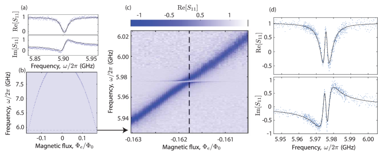
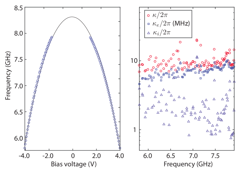
We perform our characterization measurements at the bottom plate of a dilution refrigerator at a temperature of . We probe the system by measuring the reflection spectrum through the charge port of the device (full details of the measurement setup are provided in Appendix D). In Fig. 3(a) we show a typical normalized reflection spectrum of the resonator in the linear regime, in this case tuned to a frequency of far detuned from any mechanical resonance. The reflection coefficient is , where is the coupling efficiency and is the dimensionless susceptibility (see Appendix A for details). Fitting the data to this model, we obtain and at a resonator frequency of 5.9 GHz. This frequency is more than detuned from the flux sweet spot, leading to an intrinsic linewidth that is dominated by flux noise dephasing (see Appendix B). In Fig. 3(b) we show the linear spectroscopy results for a range of values of the external magnetic flux , illustrating the DC-bias response of the resonator frequency. We infer , lying outside of our measurement band. Further, since the SQUIDs are composed of nominally identical junctions the lower frequency part of our tuning curve also lies outside of the measurement band.
We can now use the tunable response of the resonator to look for additional signatures in the spectrum. Tuning the resonance from the top of our measurement band at down to , we find a series of resonances that anti-cross with the microwave mode, largely concentrated in the range. In Fig. 3(c) we show the anti-crossing of the most strongly coupled mechanical mode we found for this device, along with a line cut at the point of minimum detuning shown in Fig. 3(d). Using the entire anti-crossing dataset, we extract the parameters of the mechanical mode by fitting the spectrum to the simple linear input-output model described in Appendix A. In the case of a single mechanical mode coupled to the readout resonator, the reflection spectrum can be written as
| (2) |
where is the dimensionless mechanical susceptibility and is the cooperativity. A least-squares fit to this model results in , and , corresponding to a mechanical quality factor . The maximum cooperativity, i.e., the ratio of the mechanical resonator’s electromagnetic read-out coupling to its intrinsic losses, approaches on resonance. Crucially, our mode lies in a “quiet” region where the closest observed mechanical modes are and below and above, respectively (see Appendix C).
In order to better understand the measured electromechanical response, we perform finite-element simulations of the full structure, simultaneously solving the equations of elasticity, electrostatics, and their coupling via piezoelectricity. Following a procedure described in Ref. Arrangoiz-Arriola and Safavi-Naeini (2016), we numerically calculate the electromechanical admittance function seen at the electrical terminals of a single phononic cavity com (2013) and generate an effective circuit using Foster synthesis Nigg et al. (2012). Using this technique we calculate coupling rates in the range for the cavity geometries present in this device, in agreement with the measurement.
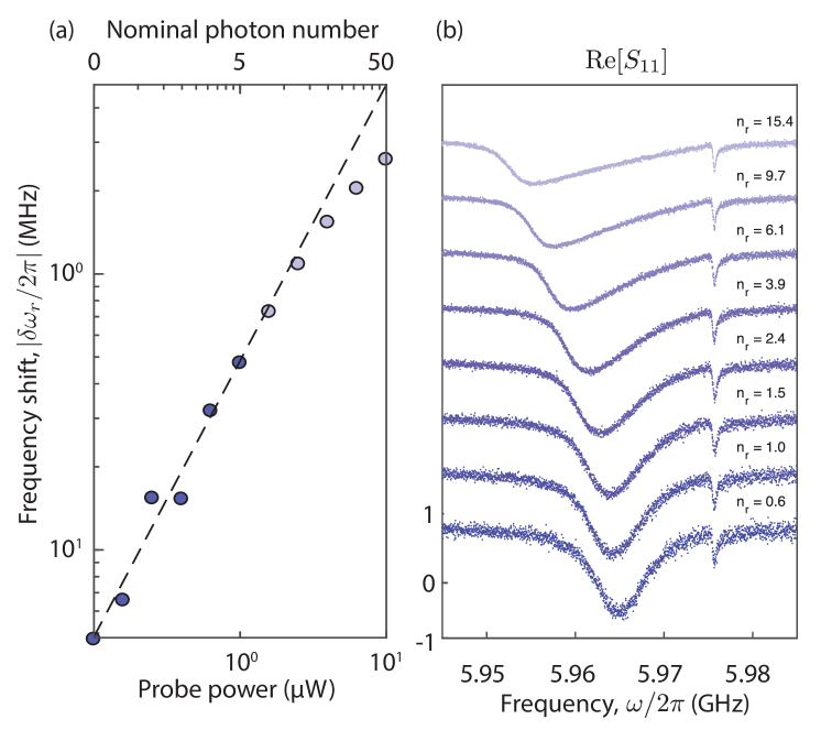
We measure the reflection spectra at higher drive power levels to verify the expected linearity of the mechanical resonance, and to distinguish it from other degrees of freedom, such as two-level systems (TLS) that have been observed in chip-scale devices Neeley et al. (2008). The strong Kerr nonlinearity of the resonator allows us to calibrate the coherently-driven photon occupation. We set the resonator frequency to , detuned from the mechanical mode, and vary the probe power. For very low powers, we can approximate the effect of the drive as a frequency shift [Fig. 4(a)] and use this to extract the photon number. For low probe powers, we observe a linear dependence of the frequency shift as expected from a linearized model in which the steady-state occupation of the resonator redshifts the frequency seen by the probe tone. However, as the probe power is increased, a more complex nonlinear response is observed as evidenced by the deviation of the estimated from the simplified linear dependence. We use the lower power points to obtain a nominal calibrated photon number , which is valid at low drive strengths and represents an upper bound to the occupation when extrapolated to stronger drives. This requires us to accurately estimate , which we do in two different ways: first using the measured resonator frequency and the normal-state junction resistance, and second by simulating the capacitance matrix of the device. Both of these methods give us nearly the same value of . We now place the resonator to the red side of the mechanical mode and change the driving strength while sweeping the probe frequency to obtain the traces shown in Fig. 4(b). We observe the microwave mode broaden and redshift as the occupation is increased to a few photons, while the mechanical mode remains unchanged. We therefore conclude that the observed resonance is not due to a TLS. Additionally, we note that the frequency and linewidth of the observed resonance remained constant over several experimental runs that involved temperature cycling the device.
IV Outlook
We have demonstrated efficient coupling between a localized phononic cavity and a superconducting microwave circuit. The cooperativity is already sufficient for efficient conversion of microwave photons to highly localized microwave phonons that can in turn be up-converted efficiently to optical photons Liang et al. (2017) – a promising route for microwave-to-optical conversion Safavi-Naeini and Painter (2010); Bochmann et al. (2013b). The performance of the device can be further improved by increasing the size of the bandgap to allow for higher mechanical . Larger phononic bandgaps lead to greater robustness to fabrication imperfections, which we believe currently limit the coherence time of the resonances (see Appendix C). In addition, optimizing the electrode placement and mode profile can lead to an increase in the coupling rate .
For quantum acoustic structures to become competitive with the best electromagnetic cavities, higher interaction rates and quality factors need to be achieved while minimizing spurious resonances to allow for fast gate operations Pechal et al. (2018). Interestingly, due to the small capacitance of the transducer and the ability to minimize crosstalk between resonances through phonon bandgap engineering, this architecture lends itself well to engineering systems where many bosonic linear modes couple to a single qubit Naik et al. (2017). Whether such a quantum acoustic approach will be competitive in the realm of quantum information processing relies on improvements in the and of the devices, which will be the focus of future work.
V Acknowledgements
We gratefully acknowledge R. Patel, C. Sarabalis, R. Van Laer, and N. Lörch for useful discussions. This work was supported by NSF ECCS-1509107, NSF ECCS-1708734, ONR MURI QOMAND, and start-up funds from Stanford University. ASN is grateful for support from Terman, Hellman, and Packard Fellowships. PAA and JDW are partially supported by the Stanford Graduate Fellowship (SGF), and MP is partially funded by the Swiss National Science Foundation postdoctoral fellowship. Device fabrication was performed at the Stanford Nano Shared Facilities (SNSF) and the Stanford Nanofabrication Facility (SNF). The SNSF is supported by the National Science Foundation under Grant No. ECCS-1542152. EAW was partly supported by an SNSF fellowship.
Appendix A Reflection spectra
We model the mechanical system as a collection of harmonic modes linearly coupled to a Kerr oscillator, which in turn is coupled to a single input/output channel for driving and readout.
The Hamiltonian of the system is
| (3) |
where is the frequency of the microwave mode, is the anharmonicity, are the frequencies of the mechanical modes, and are their coupling rates to the microwave mode. We have explicitly included a coherent driving field at frequency (which couples to the system at rate ) and bundled all other bath terms into — following a standard input-output treatment, these terms simply generate additional decay terms in the Heisenberg equations. We can eliminate the time dependence in by going into an interaction frame with respect to . The transformed Hamiltonian (now omitting the bath terms) becomes
| (4) |
where .
We can neglect the nonlinear term in the weak-drive regime where . Our experiment only measures the average output field amplitudes in steady state, given by and . These obey the Heisenberg equations of motion
| (5) | ||||
| (6) |
which can be written in the Fourier domain as
| (7) | ||||
| (8) |
We define the bare dimensionless susceptibilities
| (9) | ||||
| (10) |
where and are the total decay rates of the microwave and mechanical modes, respectively. Together with the input-output boundary condition , we can then directly solve for the reflection coefficient , and obtain
| (11) |
where is the cooperativity (or readout efficiency) for mode . We can finally assume that a single mechanical mode is relevant at a given resonator frequency , in the sense that it is the only mode that imprints a measurable signature in the reflection signal. Some algebraic manipulation leads us to the expression for
| (12) |
shown in the main text and used for fitting the data.
Appendix B Wide-band characterization of SQUID array resonator
The center frequency of the SQUID array resonator is widely tunable, allowing us to probe the the mechanical mode spectrum over a large range of frequencies. In Fig. 5 we plot the resonator frequency as a function of the bias voltage applied to run a current through the on-chip flux line (see Appendix D for details) along with a fit to the function , giving us a calibration of the external flux threading the SQUIDs. We infer that the flux-insensitive point is at and lies outside of our measurement band. At every bias point, we fit the reflection spectrum to the model derived in Appendix A (Eq. 2 with ) in order to extract the total and extrinsic resonator linewidths ( and , respectively), also shown in Fig. 5. We also define an intrinsic linewidth , which contains contributions from both energy relaxation and pure dephasing. Since our scattering parameter measurement uses only mean field amplitudes, we do not have the ability to separate these two contributions, but we can still look at the frequency dependence of in order to gain insight into the decoherence mechanisms affecting this device. We find that increases with frequency as expected from capacitive coupling to the feedline, whereas decreases as approaches the flux-insensitive point. We attribute this dependence to a strong contribution of flux-noise dephasing to the intrinsic linewidth. In fact, we see that at the mechanical frequency the intrinsic linewidth is dominated by flux noise, suggesting that the coherence times in future experiments can be improved by operating the tunable circuits near or at the flux sweet spot.
Appendix C Complete mechanical spectrum of the system
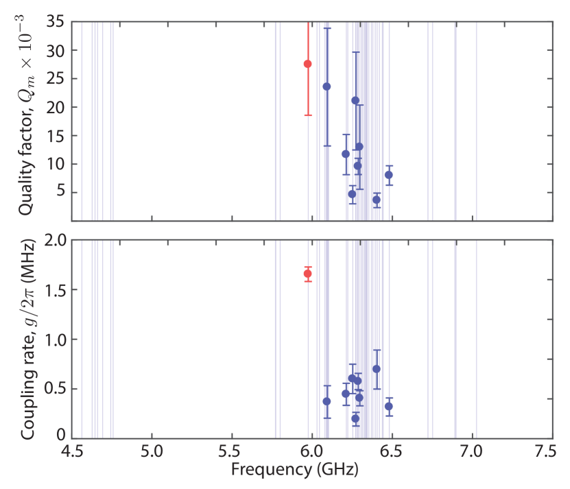
In addition to the mode at presented in the main text, we observe other modes distributed over a wide range of frequencies. In Fig. 6 we show the complete mechanical spectrum of this device. The positions of all observed modes are indicated with vertical lines, and we plot the quality factor and coupling rate of nine modes with sufficiently strong signatures in to be fit reliably to the model. The mode presented in the main text is indicated in red. Interestingly, we find that all modes have quality factors on the order of , consistent with the hypothesis that their losses are dominated by acoustic radiation, or “clamping” loss. These measurements are also consistent with previous studies of losses in phononic crystal cavities made from silicon that lack full phononic bandgaps Chan (2012). The size of the bandgap in this work is not very large ( of its center frequency according to our finite element simulations), which is of comparable magnitude to the fabrication-induced disorder in the phononic crystals. This allows trapped phonons to tunnel out of the defect region and irreversibly escape through the clamping points Chan (2012). In order to suppress this loss channel, future devices will require larger bandgaps, which can be achieved through further improvements to the design and fabrication. We also observe that with the exception of mode presented in the main text — indicated by the red point at — all modes have coupling rates on the order of . This reduction in the coupling rate has been observed in silicon optomechanical crystals as the modes are tuned outside of a bandgap region Alegre et al. (2010). In our case, finite element simulations of all six cavity geometries present in this device predict rates between , leading us to conclude that only one resonance in the spectrum is tightly confined to the defect in the way predicted by the simulations. The coupling rates can therefore be improved by engineering cavities with larger bandgaps, optimizing the geometry of the defect, and changing the placement of the electrodes.
Appendix D Experimental setup
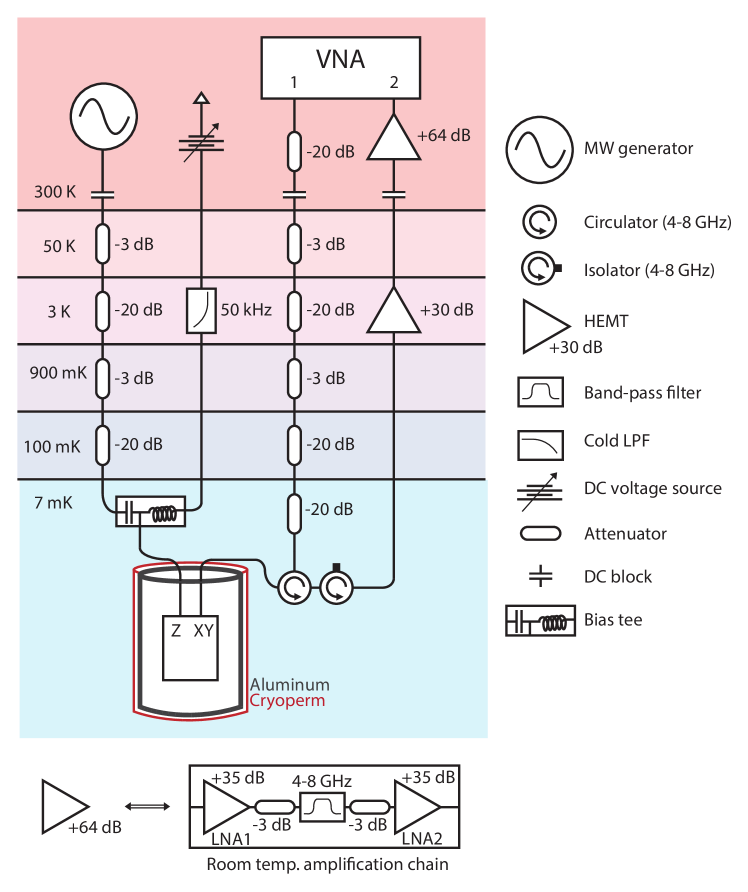
Our sample is packaged in a copper enclosure to protect it from stray radiation and limit spurious modes. The package is placed inside a multi-layer magnetic shield anchored to the mixing-chamber plate () of a cryogen-free dilution refrigerator. A Rhode & Schwartz ZNB20 vector network analyzer (VNA) generates a probe tone that is sent down to the input port of the device through a cascade of attenuators thermalized to various temperature stages of the refrigerator. A circulator (QuinStar QCY-060400C000) separates the input and output signals and an additional isolator (QuinStar QCY-060400C000) protects the device from hot () radiation in the output line. The output signal is routed up to the 3 K stage through superconducting NbTi cables, where it is amplified by a high-electron mobility transistor (HEMT) amplifier (Caltech CITCRYO1-12A). The signal is further amplified at room temperature by two low-noise amplifiers (Miteq AFS4-02001800-24-10P-4 & AFS4-00100800-14-10P-4) with a 4-8 GHz bandpass filter (Keenlion KBF-4/8-Q7S) between them before being detected at the VNA.
Flux biasing is provided by a programmable voltage source (SRS SIM928). The DC voltage passes through a cold low-pass filter (Aivon Therma-24G) at the 3 K stage and enters the DC port of a bias tee (Anritsu K250) mounted at the mixing-chamber plate. In addition an AC flux can be applied with a microwave generator (Keysight E8257D), which sends a tone to the RF port of the bias tee through an additional attenuated line, though this capability is not used in this experiment. Finally, the DC+RF output of the tee is sent directly to the flux port of the device.
References
- Hashimoto (2015) Hashimoto, RF Bulk Acoustic Wave Filters for Communications (Artech House, 2015), 1st ed.
- Devoret and Schoelkopf (2013) M. H. Devoret and R. J. Schoelkopf, Superconducting Circuits for Quantum Information: An Outlook, Science (80-. ). 339, 1169 (2013).
- O’Connell et al. (2010) A. D. O’Connell, M. Hofheinz, M. Ansmann, R. C. Bialczak, M. Lenander, E. Lucero, M. Neeley, D. Sank, H. Wang, M. Weides, et al., Quantum ground state and single-phonon control of a mechanical resonator, Nature 464, 697 (2010).
- Gustafsson et al. (2014) M. V. Gustafsson, T. Aref, A. F. Kockum, M. K. Ekstrom, G. Johansson, and P. Delsing, Propagating phonons coupled to an artificial atom, Science (80-. ). 346, 207 (2014).
- Manenti et al. (2017) R. Manenti, A. F. Kockum, A. Patterson, T. Behrle, J. Rahamim, G. Tancredi, F. Nori, and P. J. Leek, Circuit quantum acoustodynamics with surface acoustic waves, Nat. Commun. 8, 975 (2017).
- Moores et al. (2017) B. A. Moores, L. R. Sletten, J. J. Viennot, and K. W. Lehnert, Cavity quantum acoustic device in the multimode strong coupling regime (2017), eprint 1711.05913.
- Noguchi et al. (2017) A. Noguchi, R. Yamazaki, Y. Tabuchi, and Y. Nakamura, Qubit-Assisted Transduction for a Detection of Surface Acoustic Waves near the Quantum Limit, Phys. Rev. Lett. 119, 180505 (2017).
- Chu et al. (2017) Y. Chu, P. Kharel, W. H. Renninger, L. D. Burkhart, L. Frunzio, P. T. Rakich, and R. J. Schoelkopf, Quantum acoustics with superconducting qubits., Science 358, 199 (2017).
- Kervinen et al. (2018) M. Kervinen, I. Rissanen, and M. Sillanpaa, Interfacing planar superconducting qubits with high overtone bulk acoustic phonons (2018), eprint 1802.06642.
- Eichenfield et al. (2009) M. Eichenfield, J. Chan, R. M. Camacho, K. J. Vahala, and O. Painter, Optomechanical crystals, Nature 462, 78 (2009).
- Alegre et al. (2010) T. P. M. Alegre, A. Safavi-Naeini, M. Winger, and O. Painter, Quasi-two-dimensional optomechanical crystals with a complete phononic bandgap, Opt. Express 19, 5658 (2010).
- Bochmann et al. (2013a) J. Bochmann, A. Vainsencher, D. D. Awschalom, and A. N. Cleland, Nanomechanical coupling between microwave and optical photons, Nat. Phys. 9, 712 (2013a).
- Safavi-Naeini et al. (2014) A. H. Safavi-Naeini, J. T. Hill, S. Meenehan, J. Chan, S. Gröblacher, and O. Painter, Two-Dimensional Phononic-Photonic Band Gap Optomechanical Crystal Cavity, Phys. Rev. Lett. 112, 153603 (2014), eprint 1401.1493.
- Balram et al. (2015) K. C. Balram, M. Davanco, J. D. Song, and K. Srinivasan, Coherent coupling between radio frequency, optical, and acoustic waves in piezo-optomechanical circuits, Nat. Photonics 10, 1 (2015).
- MacCabe et al. (2018) G. MacCabe, H. Ren, J. Luo, J. Cohen, H. Zhou, A. Ardizzi, and O. Painter, Optomechanical Measurements of Ultra-Long-Lived Microwave Phonon Modes in a Phononic Bandgap Cavity, Bull. Am. Phys. Soc. (2018).
- Arrangoiz-Arriola and Safavi-Naeini (2016) P. Arrangoiz-Arriola and A. H. Safavi-Naeini, Engineering interactions between superconducting qubits and phononic nanostructures, Phys. Rev. A 94, 063864 (2016).
- Liang et al. (2017) H. Liang, R. Luo, Y. He, H. Jiang, and Q. Lin, High-quality lithium niobate photonic crystal nanocavities, Optica 4, 1251 (2017).
- Wang et al. (2013) R. Wang, S. A. Bhave, and K. Bhattacharjee, High kt2×Q, multi-frequency lithium niobate resonators, Proc. IEEE Int. Conf. Micro Electro Mech. Syst. pp. 165–168 (2013).
- Pop et al. (2017) F. V. Pop, S. A. Kochhar, G. Vidal-Álvarez, and G. Piazza, Laterally vibrating lithium niobate MEMS resonators with 30% electromechanical coupling coefficient, 2017 IEEE 30th Int. Conf. Micro Electro Mech. Syst. (2017).
- Vidal-Álvarez et al. (2017) G. Vidal-Álvarez, A. Kochhar, and G. Piazza, Delay Lines Based on a Suspended Thin Film of X- Cut Lithium Niobate, Ius 2017 (2017).
- Dolan (1977) G. J. Dolan, Offset masks for lift‐off photoprocessing, Appl. Phys. Lett. 31, 337 (1977).
- Stockklauser et al. (2017) A. Stockklauser, P. Scarlino, J. V. Koski, S. Gasparinetti, C. K. Andersen, C. Reichl, W. Wegscheider, T. Ihn, K. Ensslin, and A. Wallraff, Strong Coupling Cavity QED with Gate-Defined Double Quantum Dots Enabled by a High Impedance Resonator, Phys. Rev. X 7, 011030 (2017).
- Dunsworth et al. (2017) A. Dunsworth, A. Megrant, C. Quintana, Z. Chen, R. Barends, B. Burkett, B. Foxen, Y. Chen, B. Chiaro, A. Fowler, et al., Characterization and reduction of capacitive loss induced by sub-micron Josephson junction fabrication in superconducting qubits, Appl. Phys. Lett. 111, 022601 (2017).
- Girvin (2014) S. M. Girvin, in Quantum Mach. Meas. Control Eng. Quantum Syst., edited by M. Devoret, B. Huard, R. Schoelkopf, and L. Cugliandolo (Oxford University Press, 2014).
- Zhou et al. (2014) X. Zhou, V. Schmitt, P. Bertet, D. Vion, W. Wustmann, V. Shumeiko, and D. Esteve, High-gain weakly nonlinear flux-modulated Josephson parametric amplifier using a SQUID array, Phys. Rev. B 89, 214517 (2014).
- Koch et al. (2007) J. Koch, T. M. Yu, J. Gambetta, A. A. Houck, D. I. Schuster, J. Majer, A. Blais, M. H. Devoret, S. M. Girvin, and R. J. Schoelkopf, Charge-insensitive qubit design derived from the Cooper pair box, Phys. Rev. A 76, 042319 (2007).
- Eichler et al. (2014) C. Eichler, Y. Salathe, J. Mlynek, S. Schmidt, and A. Wallraff, Quantum-Limited Amplification and Entanglement in Coupled Nonlinear Resonators, Phys. Rev. Lett. 113, 110502 (2014).
- com (2013) COMSOL Multiphysics 4.4 (2013).
- Nigg et al. (2012) S. E. Nigg, H. Paik, B. Vlastakis, G. Kirchmair, S. Shankar, L. Frunzio, M. H. Devoret, R. J. Schoelkopf, and S. M. Girvin, Black-Box Superconducting Circuit Quantization, Phys. Rev. Lett. 108, 240502 (2012).
- Neeley et al. (2008) M. Neeley, M. Ansmann, R. C. Bialczak, M. Hofheinz, N. Katz, E. Lucero, A. O’Connell, H. Wang, A. N. Cleland, and J. M. Martinis, Process tomography of quantum memory in a Josephson-phase qubit coupled to a two-level state, Nat. Phys. 4, 523 (2008).
- Safavi-Naeini and Painter (2010) A. H. Safavi-Naeini and O. Painter, Design of optomechanical cavities and waveguides on a simultaneous bandgap phononic-photonic crystal slab, Opt. Express 18, 14926 (2010).
- Bochmann et al. (2013b) J. Bochmann, A. Vainsencher, D. D. Awschalom, and A. N. Cleland, Nanomechanical coupling between microwave and optical photons, Nat. Phys. 9, 712 (2013b).
- Pechal et al. (2018) M. Pechal, P. Arrangoiz-Arriola, and A. H. Safavi-Naeini, in preparation (2018).
- Naik et al. (2017) R. K. Naik, N. Leung, S. Chakram, P. Groszkowski, Y. Lu, N. Earnest, D. C. McKay, J. Koch, and D. I. Schuster, Random access quantum information processors using multimode circuit quantum electrodynamics, Nat. Commun. 8, 1904 (2017).
- Chan (2012) J. Chan, Ph.D. thesis, California Institute of Technology (2012).