Final figures for the stanene paper
First principle investigation of Tunnel FET based on nanoribbons from topological two-dimensional material
Abstract
We explore nanoribbons from topological two-dimensional stanene as channel material in tunnel field effect transistors. This novel technological option offers the possibility to build pure one-dimensional (1D) channel devices (comprised of a 1D chain of atoms) due to localized states in correspondence of the nanoribbon edges. The investigation is based on first-principle calculations and multi-scale transport simulations to assess devices performance against industry requirements and their robustness with respect to technological issues like line edge roughness, detrimental for nanoribbons. We will show that edges states are robust with respect to the presence of non-idealities (e.g., atoms vacancies at the edges), and that 1D-channel TFETs exhibit interesting potential for digital applications and room for optimization in order to improve the at the levels required by the ITRS, while opening a path for the exploration of new device concepts at the ultimate scaling limits.
Introduction
The isolation of two-dimensional (2D) flakes of graphene in 2004 Novoselov04 started a revolution, that has led to the exploration of many other 2D-materials, including Transition Metal Dichalcogenides, group III-chalcogenides, groups IVa and Va layered semiconductors MXu13 , with physical properties essentially different with respect to their three-dimensional (3D) counterparts Novoselov16 . The possibility to exploit these properties in many-body physics Li16 , or in electronics and photonics applications Fiori14 ; Srivastava15 are just some of the appeals that have fuelled the research in this area.
The family of group IVa layered semiconductors and in particular silicene Lay12 , germanene Davila14 and lastly stanene Zhu16 deserves special mention Molle17 . Differently to graphene, these materials show a slightly buckled structure, due to their larger interatomic distances, which in turns leads to strong spin-orbit interactions (SOI) and unveils the possibility of having topological phases, localized states, and ferromagnetic/antiferromagnetic nature Le14 ; Mathes14 ; Xiong16 , especially when cut in nanoribbons.
In particular, armchair stanene nanoribbons exhibit a linear dispersion relation Houssa16 , like silicene or germanene Cahangirov10 , but states are not localized at the edges Mathes14 (see Fig. S1a in Supplementary Note 1).
On the other hand, zig-zag nanoribbons do show localized states edges with a non-linear energy dispersion, and have a magnetic nature Jung09 ; Le14 ; Mathes14 ; Wang16 , which eventually leads to the formation of a bandgap. In particular, magnetism in the nanoribbons is predicted to be very dependent on the spin correlation length Yazyev10 ; Jung09 , which, at room temperature (K) is expected to be 1 nm Yazyev10 ; Jung09 . This means that nanoribbons with width smaller than the correlation length exhibit strong exchange interaction between the edges, preserving the magnetism.
Differently to non-magnetic configurations (where semi-metallic bandstructures are observed Wang16 ), in antiferromagnetic stanene nanoribbons the strong SOI can lead to the opening of a bandgap of several hundreds of meV Xiong16 (differently to germanene Mathes14 and silicene Le14 , where the bandgap is at most of few tens of meVs), that could open the path towards the exploitation in electronic applications.
A previous attempt to exploit stanene nanoribbons with semi-metallic states in a transistor leveraged the possibility of switching off the current through the scattering modulation when the current is due to non-protected states Vandenberghe17 . This ingenious proposal could however face some difficulties due to the small range of energies where the topological edge states are actually present (see Fig. S1b in Supplementary Note 1), while possibly being affected by disturbs.
Here, we theoretically explore 1D edge channels (comprised of a 1D chain of atoms) in Tunnel Field Effect Transistors (TFETs) based on a stanene zig-zag nanoribbon with an antiferromagnetic ordering. Several architectures of TFETs based on 2D materials have been investigated so far Zhao13 ; Britnell12 ; Banerjee09 ; Sarkar15 ; Li14 ; Das14 ; Roy15 , with quite distinct operational principles (ranging from a theoretical proposal based on electron-hole condensation Banerjee09 to experimental van-der-Waals heterojunctions Sarkar15 ; Roy15 ) showing heterogeneous performance. The present manuscript contributes to the efforts in this line with the first demonstration of a TFET based on a topological insulator, with localized channels at the edges. To this purpose, we employ a multiscale approach Fiori13 ; VIDES , combining different levels of physical description. In particular, Density Functional Theory (DFT) is used to calculate the electronic properties of the stanene nanoribbon, which are then exploited to define a tight-binding-like Hamiltonian expressed on a Maximally Localized Wannier Functions (MLWF) basis set Wannier ; Pizzi16 . The MLWF approach fully retains the first-principles calculations accuracy, keeping the localization of the edge states, and reducing the computational burden. The extracted Hamiltonian is then used to study 1D edge channels TFET under the non-equilibrium Green functions formalism Datta00 (solved self-consistently with 3D Poisson equation), and to explore the robustness of 1D channels against defects and the TFET performance against industry requirements.
Stanene Zig-zag antiferromagnetic nanoribbon
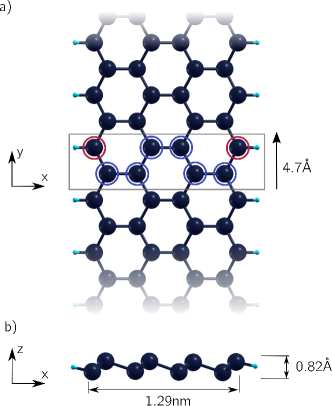
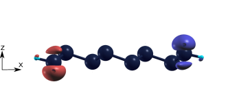
We have studied the electronic band structure of stanene antiferromagnetic zig-zag nanoribbons (ZZ-NR) through Density Functional Theory calculations by means of the Quantum Espresso suite v. 5.2.0 QE . The geometry of the nanoribbon is shown in Fig. 1, with the unit cell embedded in a grey rectangle. We have considered a ZZ-NR with a width of nm, which is expected to preserve edge magnetization consistently with the spin correlation length at room temperature calculated in Jung09 ; Yazyev10 . The ZZ-NR is passivated at the edges with H atoms, with a Sn-H bond length of Å. As mentioned above, spin orbit interaction (SOI) plays an important role in the electronic bandstructure of group IVa 2D materials, which has been here taken into account by means of a non-collinear spin polarized calculation. Out-of-plane magnetic moments are oriented in opposite directions at both edges (Fig. 2), and the in-plane magnetization is negligible. Edge atoms (defined by red circles in Fig. 1a) have a strong spin polarization, which decreases sharply toward the central atoms (defined by blue circles in Fig. 1a). The absolute magnetization of the nanoribbon is /cell (where is the Bohr magneton), and the total magnetization is zero, as corresponds to an antiferromagnetic ordering.
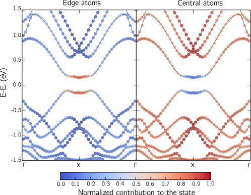
In other IVa 2D materials like graphene, germanene and silicene the origin of the antiferromagnetism in ZZ-NR has been related to the interactions of localized edge states Jung09 ; Le14 ; Mathes14 . We have checked the presence of these states in stanene by calculating the normalized contribution of the edge (Fig. 3a) and central (Fig. 3b) atoms to the density of states (DOS) projected on the bands. The conduction band minimum (CBM) is located at the point of the 1D Brillouin zone, and the valence band maximum (VBM) is located at between the and points, resulting in a indirect gap ( eV). States close to the CBM and VBM are completely localized at the edges of the nanoribbon (Fig. 3), while the central atoms contribute to the bands elsewhere (Fig. 3). As can be seen, both the conduction band (CB) and the valence band (VB) have high effective masses of and for electrons and holes, respectively, leading to a large DOS at the edges (see Fig. S4 in Supplementary Note 4), which can be interpreted as 1D channels for carrier transport.
To check this idea, and to reduce the computational requirements, we have expressed the Hamiltonian of the system on a Maximally Localized Wannier Functions (MLWF) basis set as in VIDES , exploiting the Wannier90 code Wannier . In particular, we have focused on the first four bands (per spin component) above and below the Fermi level. The main contribution to the bonding and anti-bonding states around the gap is due to -orbitals, therefore the basis transformation from Bloch states obtained from DFT to MLWF has been accomplished by initially projecting the states on the -orbitals of the Sn atoms of the unit cell, resulting into Wannier functions (per spin component) centered in their respective Sn atoms. As can be seen, the tight-binding-like Hamiltonian in the MLWF basis provides an accurate description of stanene ZZ-NR energy bands (see Fig. S2 in Supplementary Note 2).
TFET with 1D-edge channels
In the light of the previous discussion, we aim at investigating the application of the stanene ZZ-NR in 1D TFET electronic device Jena13 ; Seabaugh10 .
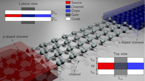
To this purpose, full 3D simulations have been performed, considering the device shown in Fig. 4. In particular, the device is a double gate Tunnel Field Effect Transistor (TFET), with top, bottom, and lateral oxides, with thicknesses given by and , respectively. If not differently stated nm and nm are considered. SiO2 has been assumed as the insulator in all cases. Source and drain regions ( nm long) are -type and -type doped, respectively, with a molar fraction, , equal to . The channel is nm long and the width is equal to nm.
Transport is assumed to be ballistic providing an upper limit of on the potential performance for the ultimate scaling limits. Non-equilibrium Green functions (NEGF) Datta00 and the 3D Poisson equation are self-consistently solved to compute charge density, potential distribution, and current through the NanoTCAD ViDES suite VIDESwww .
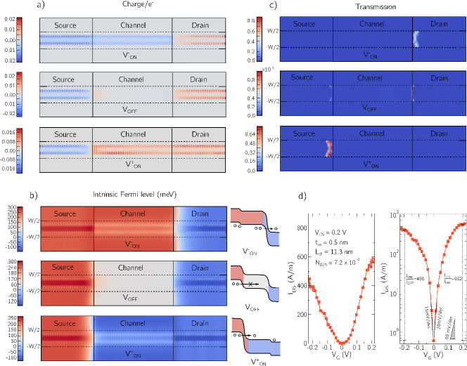
Fig. 5 shows the free charge (a) and the intrinsic Fermi level (b) for three different values of the gate voltage, , corresponding to: the OFF state (), defined as for which the minimum current is achieved (center panel); and ON state biases, , corresponding to V (bottom and top panel), respectively. The source-drain voltage, , is set to V, as required for ultra-low power operations ITRS . The width of the nanoribbon is highlighted in Fig. 5 by the ticks.
From the intrinsic Fermi level profiles (Fig. 5b) we observe that for (top panel) the channel energy nearly aligns with that of the -type source. As a result an abrupt and thin channel-to-drain barrier is formed, allowing holes in the 1D edges to tunnel from the drain CB to the source/channel VB. For (bottom panel), the energy alignment is actually the mirror symmetric, i.e., electrons in the 1D edges from the source VB tunnel through the source-to-channel barrier to the channel/drain CB. A schematic depiction of the TFET band diagram is also depicted aside the 2D colormap.
The OFF state (central panel) corresponds to the case where the channel energy gap is aligned between the source VB and drain CB forming an opaque barrier, drastically reducing the inter-band tunneling. This discussion is supported by the spatial distribution of the transmission coefficient (Fig. 5c). Indeed, for , the transmission is large (achieving values ) only either at the channel-to-drain, or at the source-to-channel junctions, while for , is extremely small ().
Free charge distribution is shown in Fig. 5a, normalized with respect to the electron elementary charge, (i.e., positive/negative magnitudes represent electrons/holes). As can be clearly seen, carriers are mostly concentrated at the 1D edges, consistently with the previous discussion. In fact, both edges contribute to the valence and conduction bands (as indicated in Fig. 3), and these two bands show spin up and spin down character (as explained in Supplementary Note 3).
In Fig. 5d, we show the transfer characteristic, vs. , both in linear and semilogarithmic scale, for a step of mV. The metal work function has been tuned in order to obtain V. As can be seen, subthreshold swings (SS), defined as the inverse slope of the vs. curve in semilogarithmic scale, equal to mV/dec and mV/dec are obtained for the and branches, respectively. The ON-OFF current ratio, (where and are defined as the currents for and , respectively), is for the -type operation and for the -type operation, due to the asymmetry of the conduction and valence bands. The SS, the ON current and the supply voltage comply with the ITRS demands. The ratio is close to the value required by high performance applications () and far from the value required for low power applications (). There is however apparent room for optimization, for example by engineering the gate length and source and drain doping Zhang14 . In Table 1, we compare the main figures of merit obtained from the present work and from TFETs based on alternative technologies Hu14 . It must be noted that differently from the rest of devices compared in Table 1, the stanene TFET shows purely 1D conduction (through 1D chains of atoms at the edges), what makes its operation markedly distinct.
| Material/Device | Ref. | |||||
|---|---|---|---|---|---|---|
| (nA/m) | (A/m) | (A/A) | (mV/dec) | (V) | ||
| Si/NW | 67 | 1 | RLuisier10 | |||
| InAs/NW | 42 | 0.3 | RConzatti12 | |||
| Si/DG | 68 | 0.3 | RDeMichielis13 | |||
| InSb/NW | 35 | 0.6 | RSylvia12 | |||
| Ge/NW | 41 | 0.3 | RLuisier10 | |||
| MoTe2/DG | 7 | 0.1 | RGhosh13 | |||
| CNT/GAA | 20 | 0.3 | RPillai13 | |||
| Bi2Se3/DG | 5 | 55 | 48 | 0.2 | RZhang14 | |
| GNR/SG | 18 | 0.1 | RBernstein12 | |||
| 1D Stanene/DG (/) | 294/573 | 15/18 | 0.2 | this work |
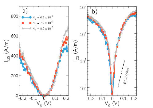
In Figs. 6, 7 and 8, we present results regarding the I-V characteristics of the stanene nanoribbon TFET, spanning among the device parameter space, i.e., considering different doping concentrations, gate oxide thicknesses and channel lengths, respectively.
In particular, three different values have been considered for the -type/-type doping of the source and the drain, i.e, , in molar fraction, equal to , and . As aforementioned, the doping is an important parameter to engineer TFET operation, since it determines the alignment of the source and drain energy bands. The extracted I/I ratio for the three devices is equal to (), (), and () in the -branch (-branch) for , , and , respectively. The small gap of the stanene nanoribbon, makes it specially sensitive to small variations in the doping of the source and drain, being the optimal value for the studied geometry.
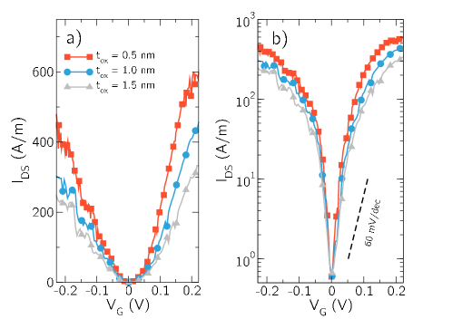
The oxide thickness (in combination with the channel thickness, ) determines the scaling length, Ferain11 , a quantitative measure of the drop of the gate electrostatic potential: the smaller the scaling length, the better the control of the gate over the channel. In this regard, the monoatomic thickness of 2D materials guarantee the minimum achievable. Better electrostatic control can then be achieve either reducing or increasing the dielectric constant of the oxide . For the 1D-edge channels TFET, the oxide thickness significantly reduces the ON current by approximately every nm for both the - and branches (Fig. 7).
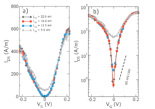
In Fig. 8, we have compared TFET transfer characteristics for three channel lengths, , nm, nm, nm and nm in order to explore the short-channel-effects (SCE) influence on the 1D channels performance. Indeed, in ultra-scale devices, source and drain contacts introduce large parasitic capacitances, undermining the effect of the gate. In addition inter-band tunneling plays a relevant role, affecting the performance in the OFF state.
As can be seen, in the case of the shortest considered channel length, a strong degradation of both the ON/OFF ratio () and the (mV/dec) is observed. For nm, is not much degraded (mV/dec), pointing out that the gate recovers the control over the channel, but the OFF state current is still degraded due to inter-band tunneling. For nm, and the OFF current are no better improved as compared to shorter channel lengths, indicating that the intrinsic properties of the material (i.e., the bandgap) are limiting the performance, and pointing out the necessity of other gate engineering solutions or scaling of the supply voltage Zhang14 .
We have previously stated that the 1D channels in the stanene ZZ-NR have opposite spin at both edges (Fig. 2 and Fig. 3). This might be thought as the main ingredient to expect protection against back-scattering. However, this not hold for ZZ-NRs with antiferromagnetic ordering. A careful look at the bands and the spins (Supplementary Note 3) shows that transitions from to are possible within the same spin component and therefore the states are not protected Manoharan10 .
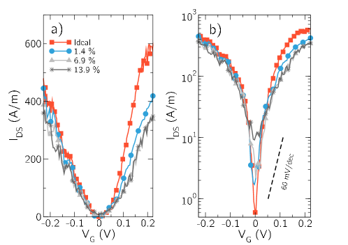
The 1D channels located at the edges of the NR and the device behavior might be strongly affected by line edge roughness (LER) Fiori07 . To check the sensitivity of the transistor operation to LER, we have calculated the transfer characteristic for different percentage of defective atoms at the edges (Fig. 9 and Methods). As can be seen, despite the large number of defects, I preserved and decreases with respect to the ideal case at most by only a factor of () for the -type (-type) branch. Transport results are in good agreement with DFT calculations (Fig. S5 in Supplementary Note 5), where we have demonstrated that localized edge states are conserved, when different number of edge atoms are removed.
The less pronounced degradation of the ON current for the -type conductive branch, might be due to the fact that VB has a non-negligible contribution of the central atoms around its maxima (Fig. 2). The OFF state current, on the contrary, is more affected by the presence of defects increasing by a factor in comparison with the ideal case, what as explained in a previous work might be due to appearance of mid-gap statesYoon08 . The sub-threshold swing , is consequently affected, shifting from the sub-thermionic values mV/dec (mV/dec) for the ideal case, to the over-thermionic values mV/dec (mv/dec) for the highest percentage of defects in the -branch (-branch). Smaller number of defects still preserves sub-thermionic equal to mV/dec (mV/dec) and mV/dec (mV/dec) for and percentages in the -branch (-branch), respectively.
Conclusion
The combination of localized edge states and energy gap that arises from the antiferromagnetic ordering in group IVa nanoribbons, opens a new path for the exploration of electronic devices. We have investigated tunneling field effect transistors based on stanene zig-zag nanoribbons, with purely 1D channels for both electrons and holes. The potential performance of the 1D channels TFET has been assessed by a comprehensive multiscale study combining the predictive power of Density Functional Theory calculations, the computational efficiency of tight-binding Hamiltonians obtained by means of Maximum Localized Wannier Functions, and full self-consistent device simulations based on non-equilibrium Green functions and 3D Poisson equation. Our results show that the 1D edge channels are robust against line-edge roughness and that they show interesting performance against industry requirements, although the small bandgap of stanene demands gate and doping optimization to achieve compliant ratio.. The proposed study theoretically demonstrate for the first time the full operation of 1D edges TFETs based on stanene nanoribbons, opening the path towards 1D ultra-scale devices.
Methods
Density Functional Theory. First principle calculations have been performed using Density Functional Theory as implemented in Quantum Espresso v. 5.2.0 QE . Supercells with Å and Å of vacuum in the -direction (namely the NR width) and -direction (namely orthogonal to the NR plane) were used to minimize the interaction between periodic repetitions of the cell. A structural optimization of all geometries was performed within the Broyden-Fletcher-Goldfarb-Shanno algorithm until forces were less than eVÅ. The convergence for energies was set to eV. A Perdew-Burke-Ernzerhof exchange-correlation functional (Generalized Gradient Approximation) was considered PBE within fully-relativistic norm-conserving pseudopotentials including non-collinear corrections. The pseudopotentials were obtained from the SSSP Library, for both Sn and H SSSP . Energy cutoffs for charge density and wavefunction expansions were set to Ry and Ry, respectively. SOC was included in the self-consistent calculations of the charge density. Integration in the Brillouin zone was accomplished in a -centered grid for the ZZ-NR, whilst a -centered grid was considered for the 9-unit-cell NRs discussed in the Supporting Information. The band-structure calculations were performed for a -points -grid on a highly symmetric path, --, along the 1D Brillouin zone.
Maximally Localized Wannier Functions. Wannier90 suite v. 2.0.1 Wannier was used to compute the Maximally Localized Wannier Functions (MLWFs). The same -sampling of the Brillouin zone as in the DFT simulations has been used to compute the overlap matrices required to determine the MLWFs. 16 bands around the fundamental gap have been considered (including spin degeneration). A threshold of Å2 was set for the total spread change in the MLWFs in consecutive iterations. Initial projection on -type orbital centered on each of the Sn atoms were considered for the Wannierisation. The band-structure was then calculated on a denser -grid, , along the same -- path as in DFT.
Transport simulations. Device transport simulations were performed with the NanoTCAD ViDES code VIDES ; VIDESwww . Non-equilibrium Green functions (NEGF) and three-dimensional (3D) Poisson equation were self-consistently solved, under varying bias conditions, with a step of mV, determining the device electrostatic potential, charge density, and current in the ballistic regime at room temperature ( K). The MLWF Hamiltonian with up to 96 nearest-neighbors was used to compute NEGF within a energy step of meV and a energy window ranging from eV to eV (below/above the Fermi level at the source). For Poisson, the mean position of the MLWF was taken as representative of the location of the charge center. In order to deal with a reasonably discretized grid, charge centers were grouped, inside the unit cell, into grid points along the -direction with squeezed and coordinates. A resulting uniform grid was used in the 3D Poisson for the channel length of nm. Convergence in the self-consistent calculation was accomplished when the change in the potential at any grid point was less than V. Line edge roughness was simulated by introducing arbitrary defects along the edges of the NR channel. The on-site energies of the Hamiltonian corresponding to MLWF where a defect was introduced were forced to a large constant value of energy emulating this way the presence of a barrier. An additional check consist of setting the coupling terms to this site in the Hamiltonian to zero, thus removing the possibility of hopping. This methodology leads to equivalent results (see Supplementary Information) but it is less stable in terms of convergence.
Acknowledgments
Authors gratefully acknowledge the support from the Graphene Flagship (No. 696656).
Supplementary information
Supplementary Information accompanies this paper.
References
- (1) Novoselov, K. S., Geim, A. K., Morozov, S. V., Jiang, D. , Zhang, Y. , Dubonos, S. V., et al. Electric field effect in atomically thin carbon films. Science, 306, 666. 2004
- (2) Xu, M., Liang, T. , Shi, M., and Chen, H. Graphene-like two-dimensional materials. Chem. Rev., 113, 3766. 2013.
- (3) Novoselov, K. S., Mishchenko, A., Carvalho, A., and Castro-Neto, A. H. 2D materials and van der Waals heterostructures. Science, 353, 6298. 2016.
- (4) Li, L., Farrell, E. C. T. O., Loh, K., Eda, G., Ozyilmaz, B., and Castro Neto, A. H. Controlling many-body states by the electric-field effect in a two-dimensional material. Nat. Phys., 529, 185. 2016.
- (5) Fiori. G. Bonaccorso, F., Iannaccone, G., Palacios, T., Neumaier, D., Seabaugh, A., et al. Electronics based on two-dimensional materials. Science, 9, 769. 2014.
- (6) Srivastava, A., Sidler, M., Allain, A. V., Lembke, D. S., Kis, A., and Imamoǧlu, A. Optically active quantum dots in monolayer WSe2. Nat. Nanotech. 10, 491. 2015
- (7) Vogt, P., de Padova, P., Quaresima, C., Avila, J., Frantzeskakis, E., Asensio, M-C., et al. Silicene: compelling experimental evidence for graphene-like two-dimensional silicon Phys. Rev. Lett., 108, 155501. 2012.
- (8) Davila, M.E., Xian, L., Cahangirov, S., Rubio, A., and Le Lay, G. Germanene: a novel two-dimensional germanium allotrope akin to graphene and silicene New J. Phys., 16, 095002. 2014.
- (9) Zhu, F., Chen, W., Xu, Y., Gao, C., Guan, D., Liu, C., et al. Epitaxial growth of two-dimensional stanene. Nat. Mater., 14, 1020. 2015.
- (10) Molle, A., Goldberger, J., Houssa, M, Xu, Y., Zhang, S-C., and Akinwade, D. Buckled two-dimensional xene sheets. Nat. Mat., 16, 163. 2017.
- (11) Mathes, L., and Bechstedt, F. Influence of edge and field effects on topological states of germanene nanoribbons from self-consistent calculations, Phys. Rev. B, 90, 165431. 2014.
- (12) Le, N. B., Huan, T. D., Woods, L. M. Tunable Spin-dependent properties of zig-zag silicene nanoribbons Phys. Rev. Appl., 1, 054002. 2014.
- (13) Xiong, W., Xia, C., Peng, Y., Du, J., Wang, T., Zhang, J., et al. Spin-orbit coupling effects on electronic structures in stanene nanoribbons. Phys. Chem. Chem. Phys., 18, 6534. 2016.
- (14) Houssa, M., van de Broek, B., Iordanidou, K., Lu, A. K. A., Pourtois, G., Locquet, J. P., et al. Topological to trivial insulating phase transition in stanene. Nano Research, 9, 774. 2016.
- (15) Cahangirov, S., Topsakal, M., and Ciraci1, S. Armchair nanoribbons of silicon and germanium honeycomb structures. Phys. Rev. B, 81, 195120. 2012.
- (16) Jung, J., Pereg-Barnea, T., and MacDonald, A.H. Theory of interedge superexchange in zig-zag edge magnetism. Phys. Rev. Lett., 102,, 227205. 2009.
- (17) Wang, T-C., Hsu, C-H., Huang, Z-Q., Chuang, F-C., Su, W-S., and Guo, G-Y. Tunable magnetic states on the zig-zag edges if hydrogenated and halogenated group-IV nanoribbons. Sci. Rep., 6, 39083. 2016.
- (18) Yazyev, O. V. Emergence of magnetism in graphene materials and nanostructures. Rep. Prog. Phys., 73, 056501. 2010.
- (19) Vandenberghe, W. G., and Fischetti, M. V. Imperfect two-dimensional topological insulator field-effect transistors. Nat. Commun., 8, 14184. 2017
- (20) Zhao, P., Feenstra, R.M., Gu, G. and Jena, D., 2013. SymFET: A proposed symmetric graphene tunneling field-effect transistor. IEEE Transactions on Electron Devices, 60, 951. 2013.
- (21) Britnell, L., Gorbachev, R.V., Jalil, R., Belle, B.D., Schedin, F., Mishchenko, A., Georgiou, T., Katsnelson, M.I., Eaves, L., Morozov, S.V. and Peres, N.M.R. Field-effect tunneling transistor based on vertical graphene heterostructures. Science, 335, 947. 2012.
- (22) Banerjee, S.K., Register, L.F., Tutuc, E., Reddy, D. and MacDonald, A.H. Bilayer pseudospin field-effect transistor (BiSFET): A proposed new logic device. IEEE Electron Device Letters, 30, 158-160. 2009.
- (23) Roy, T., Tosun, M., Cao, X., Fang, H., Lien, D.H., Zhao, P., Chen, Y.Z., Chueh, Y.L., Guo, J. and Javey, A. Dual-gated MoS2/WSe2 van der Waals tunnel diodes and transistors. ACS Nano, 9, 2071. 2015.
- (24) Sarkar, D., Xie, X., Liu, W., Cao, W., Kang, J., Gong, Y., Kraemer, S., Ajayan, P.M. and Banerjee, K. A subthermionic tunnel field-effect transistor with an atomically thin channel. Nature 526, 91. 2015.
- (25) Li, M., Esseni, D., Snider, G., Jena, D. and Grace Xing, H. Single particle transport in two-dimensional heterojunction interlayer tunneling field effect transistor. Journal of Applied Physics, 115, 074508. 2014
- (26) Das, S., Prakash, A., Salazar, R. and Appenzeller, J. Toward low-power electronics: tunneling phenomena in transition metal dichalcogenides. ACS nano, 8(2), pp.1681-1689.
- (27) Fiori, G., and Iannaccone, G. Multiscale modeling for graphene-based nanoscale transistors. Proceedings IEEE 101, 1653. 2013.
- (28) Bruzzone, S., Iannaccone, G., Marzari, N., Fiori, G. An open-source multiscale framework for the simulation of nanoscale devices. IEEE Trans. Electron Devices, 61, 48. 2014.
- (29) Marzari, N., Mostofi, A. A., Yates, J. R., Souza, I., Vanderbilt, D. Maximally localized Wannier functions: theory and applications. Rev. Mod. Phys., 84, 1419. 2012.
- (30) Pizzi, G., Gibertini, M., Dib, E., Marzari, N., Iannaccone, G., and Fiori, G. Performance of arsenene and antimonene double-gate MOSFETs from first principles. Nat. Commun., 7, 1. 2016.
- (31) Datta, S. Nanoscale device modeling: the Green’s function method. Superlattices Microstruct., 28, 253. 2000.
- (32) Giannozzi, P., Baroni, S., Bonini, N., Calandra, M., Car, R., Cavazzoni, C., et al. QUANTUM ESPRESSO: a modular and open-source software project for quantum simulation of materials. J. Phys.: Cond. Matt., 21, 395502. 2009.
- (33) Jena, D. Tunneling transistors based on graphene and 2D crystals. Proc. IEEE, 101, 1585. 2013.
- (34) Seabaugh, A., Zhang, Q. Low-voltage tunnel transistors for beyond CMOS logic. Proc. IEEE, 98, 2095. 2010.
- (35) Nano TCAD ViDES. 2017, available at: http://vides.nanotcad.com/vides/.
- (36) International Technology Roadmap for Semiconductors (ITRS) 2.0. 2015 edition, available at: http://www.itrs2.net.
- (37) Ferain, I., Colinge, C.A. and Colinge, J.P. Multigate transistors as the future of classical metal-oxide-semiconductor field-effect transistors. Nature, 479, 310. 2011.
- (38) Lu, H. and Seabaugh, A. Tunnel field-effect transistors: State-of-the-art. IEEE Journal of the Electron Devices Society, 2, 44. 2014
- (39) Luisier, M. and Klimeck, G. Simulation of nanowire tunneling transistors: From the Wentzel–Kramers–Brillouin approximation to full-band phonon-assisted tunneling. Journal of Applied Physics, 107, 084507. 2010.
- (40) F., Pala, M.G., Esseni, D., Bano, E. and Selmi, L. Strain-induced performance improvements in InAs nanowire tunnel FETs. IEEE Transactions on Electron Devices, 59, 2085. 2012
- (41) De Michielis, L., Lattanzio, L., Moselund, K.E., Riel, H. and Ionescu, A.M. Tunneling and occupancy probabilities: How do they affect tunnel-FET behavior?. IEEE Electron Device Letters, 34, 726. 2013
- (42) Sylvia, S.S., Khayer, M.A., Alam, K. and Lake, R.K. Doping, tunnel barriers, and cold carriers in InAs and InSb nanowire tunnel transistors. IEEE transactions on electron devices, 59, 2996. 2012
- (43) Ghosh, R.K. and Mahapatra, S. Monolayer transition metal dichalcogenide channel-based tunnel transistor. IEEE Journal of the electron devices society, 1, 175. 2013
- (44) Pillai, P.B., Umari, P. and De Souza, M.M. Are carbon nanotubes still a viable option for ITRS 2024?. International Electron Devices Meeting (IEDM), 32. 2013.
- (45) Zhang, Q., Iannaccone, G. and Fiori, G., 2014. Two-Dimensional Tunnel Transistors Based on Bi2Se3 Thin Film. IEEE Electron Device Letters, 35, 129, 2014.
- (46) Bernstein, K., Cavin, R.K., Porod, W., Seabaugh, A. and Welser, J. Device and architecture outlook for beyond CMOS switches. Proceedings of the IEEE, 98, 2169. 2012
- (47) Manoharan, H. C. Topological insulators: a romance with many dimensions. Nat. Nanotech., 5, 477. 2010.
- (48) Fiori, G., and Iannaccone, G. Simulation of graphene nanoribbon field-effect transistors. IEEE Electron Dev. Lett., 28, 760. 2007.
- (49) Yoon, Y., Fiori, G., Hong, S., Iannaccone, G. and Guo, J. Performance comparison of graphene nanoribbon FETs with Schottky contacts and doped reservoirs. IEEE Transactions on Electron Devices, 55, 2314. 2008.
- (50) Deretzis, I., Fiori, G., Iannaccone, G., Piccitto, G. and La Magna, A. Quantum transport modeling of defected graphene nanoribbons. Physica E: Low-dimensional Systems and Nanostructures, 44, 981. 2012.
- (51) Perdew, J. P., Burke, K., Ernzerhof, M. Generalized gradient approximation made simple. Phys. Rev. Lett., 77, 3865. 1996.
- (52) Standard Solid State Pseudopotentials (SSSP). http://www.materialscloud.org/sssp. 2017.
- (53) Ezawa, M., and Nagaosa, N. Interference of topologically protected edge states in silicene nanoribbons. Phys. Rev. B, 88, 121401. 2013.