On the Nature of Trapped-Hole States in CdS Nanocrystals and the Mechanism of their Diffusion
Abstract
Recent transient absorption experiments on CdS nanorods suggest that photoexcited holes rapidly trap to the surface of these particles and then undergo diffusion along the rod surface. In this paper, we present a semiperiodic DFT model for the CdS nanocrystal surface, analyze it, and comment on the nature of both the hole-trap states and the mechanism by which the holes diffuse. Hole states near the top of the valence band form an energetic near continuum with the bulk, and localize to the non-bonding sp3 orbitals on surface sulfur atoms. After localization, the holes form nonadiabatic small polarons that move between the sulfur orbitals on the surface of the particle in a series of uncorrelated, incoherent, thermally-activated hops at room temperature. The surface-trapped holes are deeply in the weak-electronic coupling limit and, as a result, undergo slow diffusion.
In semiconductor colloidal nanocrystals, surface traps play a pivotal role in deciding the fates of photoexcited carriers. Despite their importance, the microscopic nature and character of the trapped states remains elusive. In cadmium-chalcogenide systems like CdS and CdSe, electron and hole traps form on the surface.1, 2, 3, 4, 5, 6, 7, 8, 9, 10, 11 In most syntheses, capping ligands form bonds with the cadmium atoms at the surface and turn electron trapping into a minor decay pathway.5, 10, 12, 13, 14, 15 In contrast, chalcogen atoms at the surface often remain undercoordinated and participate in hole trapping.16, 17, 4, 9, 10, 11, 18 The valence band holes in these materials exhibit sub-picosecond lifetimes, the quantum yield for band gap photoluminescence is low, and there is a relatively strong emission from recombination between trapped holes and conduction band electrons.19, 16, 20, 17, 5, 6, 21, 22, 23, 24 The energies of the hole states relative to the bulk valence band and the extent of wavefunction localization within the trapped states of nanocrystals have been inferred from experimental spectra, though calculations for small clusters do exist.25, 9, 11, 10 Recent work by Utterback et al.26 makes the picture richer, showing that trapped holes are not static, but are mobile at room temperature. That work showed that a one-dimensional diffusion-annihilation model could explain the long-lived power law decays in transient absorption spectra, and hypothesized that hole diffusion occurs through hopping, where hops are on the order of individual bond lengths. Deducing the mechanism for this hole motion and testing the hypothesis put forward in Ref. 26 is a principal goal of this manuscript.
In this work, we use density functional theory (DFT) to describe the atomic structure of the nanocrystal surface and bulk states of CdS and the electronic structure of the trapped holes in the material. We analyze the electronic structure of bulk and surface states within the system, and by parameterizing a tight-binding Hamiltonian from the DFT data, put forward a mechanism for the motion of trapped holes on the surface by computing hole hopping rates using Holstein small polaron/nonadiabatic Marcus theory. We show that the rates are related to an anisotropic diffusion coefficient, and from the rate theory, propose a lower bound on the reorganization energy for hole hopping that is consistent with the experimental data reported in Ref. 26.
As Fig. 1A illustrates, CdS nanorods exhibit 6 identical faces, with all facets characterized by the Miller-Bravais index.27, 12, 28
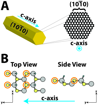
On this surface, both cadmium and sulfur atoms make three bonds to the crystal lattice, leaving one orbital on the atoms exposed to the surface to be either passivated by a ligand or left as a dangling bond.
To construct a computational model for the CdS bulk and surface where ligands passivate cadmium but not sulfur on the surface26, we begin by optimizing the nuclear positions of a wurtzite supercell in the bulk phase by minimizing the energy, changing both atomic positions and cell dimensions, at constant stress. To build the surface “slab” supercell from the bulk wurtzite cell, we use the fact that a wurtzite crystal cleaved along the direction has an orthorhombic symmetry,27, 29 with the sulfur atoms forming a rectangular lattice along in the orthorhombic x-y plane for CdS (Fig. 1B). We choose coordinates so that the orthorhombic x-y plane coincides exactly with the wurtzite crystal b-c plane. From the bulk supercell, we form the surface slab by replicating the bulk cell along the orthorhombic z-axis. It is convenient to define a layer as comprising 8 atoms of cadmium and 8 atoms of sulfur (Fig. 1B) lying approximately in the orthorhombic x-y plane. The results reported here use an 8-layer slab supercell, unit cells in size, though the SI provides extensive convergence tests as a function of supercell dimensions. This supercell generates two equivalent, but independent, surfaces separated by a bulk phase of CdS sandwiched between the surfaces in a “middle-out” geometry. Finally, placing a vacuum layer 30 Å thick normal to the surface allows plane-wave basis functions and periodic boundary conditions to be applied in all directions, but ensures that periodic images in the z-direction do not interact with one another.
We use pseudo-hydrogen potentials30, 31 bonded to all surface cadmium sites to saturate the dangling bonds on cadmium atoms and mimic the effect of ligand passivation. To model the appropriate experimental systems, we leave surface sulfur atoms unpassivated. We then find the equilibrium nuclear positions for the slab by minimizing the energy, changing atomic positions at fixed supercell dimensions. The positions of the atoms in the middle 2 layers of the slab remain fixed during surface relaxation to simulate a rigid bulk region, though after relaxation the constraint forces on these atoms are zero to within accepted tolerance (23 meV/Å). This implies that the middle 2 layers appear approximately as bulk to the other atoms, whose positions we allow to change until their atomic forces have magnitudes less than 10 meV/Å.
Fig. 2A shows the total density of states (DOS) of the slab around the Fermi energy, .
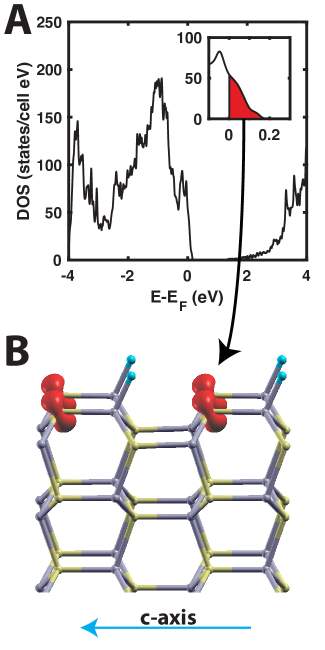
In these calculations, identifies the energy at which the bands become half filled, similar to in a metal at finite temperatures. At energies below , the electron population dominates, while at energies above , the hole population dominates. The inset to the DOS in Fig. 2A shows the region above but below the band gap, representing the lowest-energy hole states. Fig. 2B shows the orbital density corresponding to the lowest energy hole states, which are clearly localized to the surface. This density looks like it could be formed from a linear combination of sp3 hybridized orbitals, centered at the sulfur atoms located on the surface. Indeed, as we will show below, this observation provides the basis for a quantitative tight-binding model for the surface hole states. Constraining the energy window to lie within meV above or below , to focus on the thermally accessible hole states, does not change the picture for the orbitals in Fig. 2B qualitatively.
Other electronic structure calculations of small CdS and CdSe clusters have reported that hole states are localized to the sulfur atoms on the surface, in agreement with this work.11, 10, 25, 9 Unlike those calculations, however, our hole states are not well separated from the bulk DOS, but rather form a continuum with the highest fully-occupied (by electrons) states. This result is consistent with the experimental work of Mooney et al.,22 which finds that bulk and surface states can be separated by merely tens of meV.
The continuous density of states in the vicinity of the highest occupied valence bands, shown as the inset in Fig. 2A, implies that holes prepared in the bulk rapidly move to the surface, lowering their energy by accessing a tier of intermediate states that are separated by infinitesimally small amounts of energy. This result supports experimental reports on CdS nanocrystals, which find that hole trapping to the surface occurs on the timescale of picoseconds 21, 19, 16, 17, 26.
At first blush, the data in Fig. 2 seem to imply that the hole states are delocalized across sulfur atoms on the surface. But one must keep in mind the limitations of adiabatic electronic structure theory, which gives the solutions to the electronic structure problem in the Born-Oppenheimer approximation at zero absolute temperature. Similar to constructing molecular orbitals from linear combinations of atomic orbitals, if two orbitals are coupled, even weakly, DFT will yield adiabatic states that are delocalized superpositions.32 But if the electronic coupling is weak relative to the coupling between the electrons and the environment, this delocalization will not survive decoherence from thermal fluctuations at finite temperature.33, 34 Thermal decoherence in the electronic space will produce localized states that, while not eigenstates of the electronic Hamiltonian, more closely resemble the eigenstates of the system plus the environment.
The calculations presented here do not explicitly include solvent, ligand, or electron-phonon coupling. While it is computationally infeasible to include them directly into the electronic structure calculations, we can include their effects by constructing a model Hamiltonian. We begin by quantizing the electron density in terms of the sp3 orbitals on all sulfur atoms. This leads to a tight-binding Hamiltonian, , whose diagonal elements are the on the on-site energies, , and the off-diagonal elements are the tunneling matrix elements, , where the subscripts denote the sp3 orbitals of the sulfur atoms. We use Wannier localization to generate the orbitals and compute the matrix elements. Fig. 3 shows that, indeed, diagonalizing and forming the two-dimensional band structure for the directions conjugate to the x-y orthorhombic axes yields a band structure that is indistinguishable from the adiabatic solution to the electronic structure near the valence band maximum, where the surface hole states dominate.
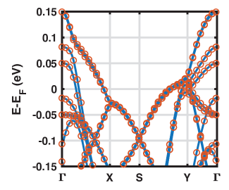
At zero temperature and in the absence of electron-phonon coupling, the adiabatic solution corresponding to the eigenvalues and eigenstates of would be an accurate solution to the electronic problem. But the energies of the relevant tunneling matrix elements for hole transport, described in more detail below and reported in detail in the SI (Tables S1-S2), are on the order of or are smaller than at room temperature, implying that thermal fluctuations of the nuclei do indeed destroy coherence between orbitals and collapse the band structure in Fig. 3.35, 33
To construct a model Hamiltonian that captures these effects at the level of a linear response theory, we project out the surface sulfur atoms from , giving an effective two-dimensional tight-binding Hamiltonian for the holes on the surface, . The system-bath Hamiltonian, , which couples the surface electronic degrees of freedom to the phonons, ligands, and solvent, is linear in the electron density, , where is the electrostatic potential of the nuclei.35, 33 The electron density, quantized in the mutually-orthogonal Wannier sp3 orbitals, , is . Assuming that all nuclei undergo harmonic vibrations about their equilibrium positions and expanding to linear order in all bath modes leads to the Holstein small-polaron Hamiltonian, where the nuclear motions comprise a heat bath,
| (1) |
Here, () is the fermionic creation (annihilation) operator that puts (removes) a hole in orbital , () is the bosonic creation (annihilation) operator for bath mode , is the coupling matrix element between mode and electronic orbital , and is the energy of bath mode . The sum over and goes over non-bonding orbitals of nearest- and next-nearest-neighbors on the surface. Fig. 4A shows one of these orbitals.
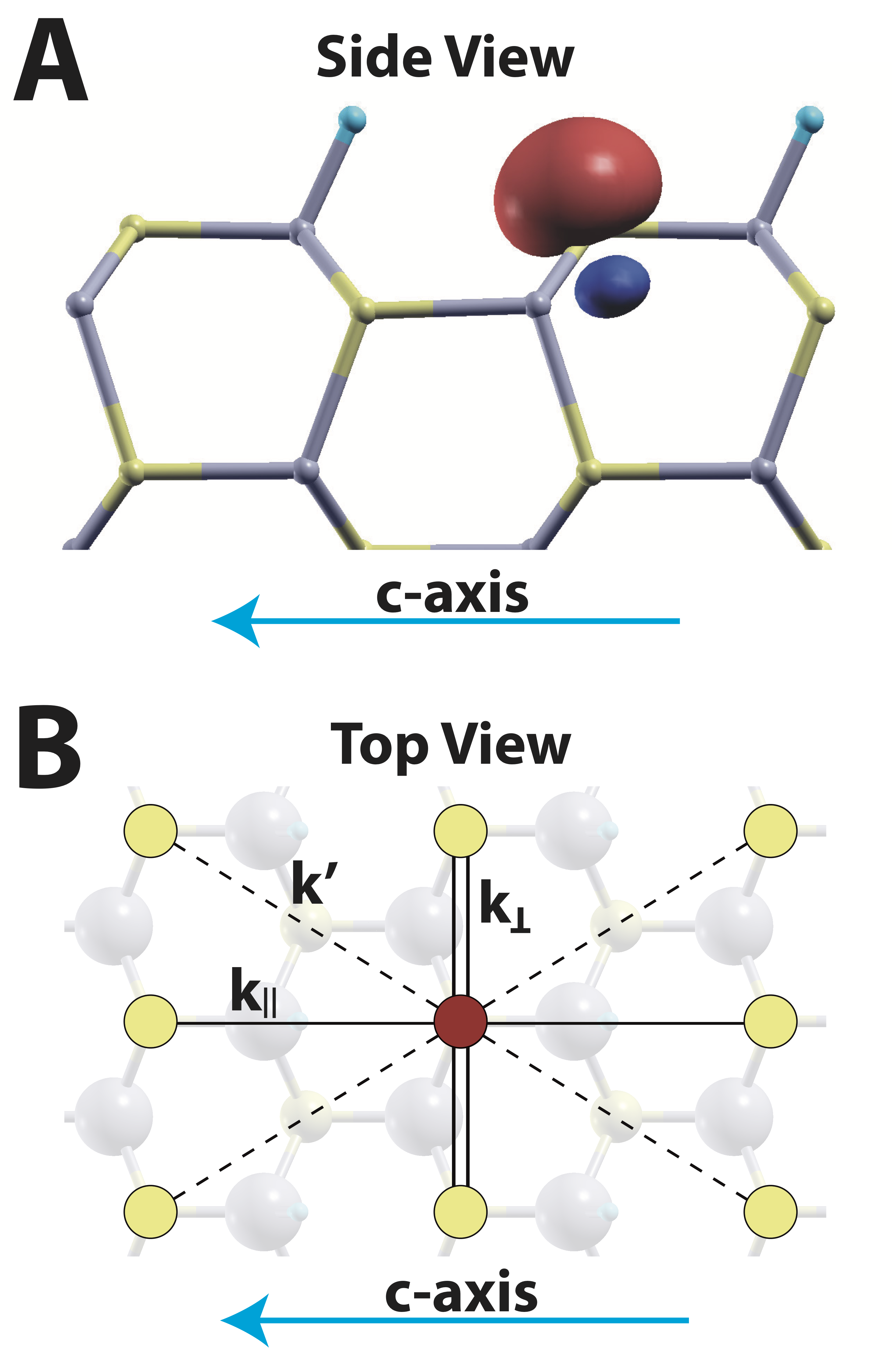
The relevant tunneling matrix elements for hole transfer down the crystal c-axis are and , corresponding to the tunneling matrix elements between nearest- and next-nearest-neighbors along the rod axis, respectively (Fig. 4B). Our calculations for and yield meV. These small values for the tunneling matrix elements, compared to both room-temperature and to characteristic values for ,35, 33 place this system squarely in the weak electronic coupling limit, where bath fluctuations destroy the band structure and localize holes to orbitals on individual sulfur atoms. In this limit, the hole populations on the surface sites obey the quantum Master equation,
| (2) |
with rates given by the Golden Rule, . In the high temperature limit, which is the simplest approximation, bath energies are much less than , and the detailed spectrum of the heat bath is irrelevant. One then recovers the Marcus expression36 for nonadiabatic hole transfer between degenerate states,
| (3) |
where is the reorganization energy. As implied earlier by our notation, and correspond to the rates and , respectively (Fig. 4B). Finally, an asymptotic expansion of Eq. 2, presented in the SI (Sec. S.1), gives a Fokker-Planck approximation to the master equation, which is an anisotropic diffusion equation. The diffusion constant for hole hopping along the axis of the nanorod, , is
| (4) |
where Å is the surface sulfur-to-sulfur distance parallel to the long axis of the nanorod. Note that , the hopping rate along the diagonal line connecting next-nearest-neighbors (Fig. 4B), makes a significant contribution to . The factor of two in Eq. 4 reflects the fact that there are two next-nearest-neighbors for each nearest-neighbor on the rectangular lattice, in the direction of the crystal c-axis.
Calculating is not an objective of this manuscript, nor is it computationally feasible in a system of this size. Without a value for , we cannot compute the diffusion constant , but we can use our computed hopping matrix elements, meV, in conjunction with experimental data to bound the value of . Utterback et al.26 measured an upper bound for to be 10-7 cm2s-1. From this bound on and our calculated values of and , we use Eq. 3-4 find a lower bound for of 1 eV. This value of is large for electron transfer reactions in solution, but not uncommon for polaron hopping transport in polar semiconductors, where lattice phonons couple strongly to the electronic degrees of freedom.37, 22 Similarly, the high-temperature approximation to the system-bath coupling, while appropriate for a wide class of electron transfer reactions in solution, may need to be revised as more information about the specific coupling to lattice phonons and to nuclear distortions of the ligands, whose energies are not necessarily small relative to 22, becomes available. The tunneling matrix element for hopping perpendicular to the crystal c-axis, meV (Fig. 4B), is about an order of magnitude larger than . Because it is still much smaller than , so the holes still remain small polarons localized to atomic sites, not delocalized around the waist of the rod.
In summary, we have presented an atomistic computational model to capture the electronic structure of the bulk and surface states of CdS nanorods. The adiabatic solution to the electronic structure of this surface slab clearly shows hole states, near the Fermi energy, that are localized to the undercoordinated sulfur atoms on the surface. Our results show that the hole states of a CdS surface slab form a near continuum with the bulk states of electrons, a result that differs from previous theoretical work on small quantum dots,11, 10, 25, 9 but is consistent with recent experimental work of Mooney et al.22 The continuous density of states between holes and electrons would also rationalize a wealth of experimental data that finds holes prepared in the bulk relax quickly to the surface.21, 19, 16, 17, 26 The densities of states for small clusters of CdS, which sometimes show trapped states that are well-separated from the valence band,11, 10, 25, 9 differ from the density of states for the nanocrystal model presented here.
Motivated by the adiabatic electronic structure results, we parameterize a model tight-binding Hamiltonian from the sp3 orbitals centered on sulfur atoms. The calculated tunneling matrix elements between relevant sulfur orbitals on the surface are small relative to the estimated reorganization energy, so that thermal fluctuations and nuclear motions localize holes into small polarons, trapped in non-bonding sulfur orbitals on the surface. While we cannot rule out hole hopping through a super-exchange mechanism, mediated through virtual bulk or ligand states, it is notable that this mechanism need not be invoked. Because CdS nanocrystals in conventional syntheses are so deep in the weak electronic coupling regime, hole transport in these particles is slow at room temperature. Our results give direct support for the picture presented by Utterback et al.26, who hypothesized that holes diffuse by hopping on length scales comparable to interatomic spacings.
1 Computational Methods
The DFT calculations employed the Vienna Ab initio Simulation Package38, 39, 40, 41, a plane-wave electronic structure code. We used the projector augmented wave method with the Perdew-Burke-Erzhenhoff generalized gradient approximation for the exchange-correlation functional,42, 43 which for CdS strikes a reasonable balance between computational feasibility and accuracy. The cadmium 5s24d10 and sulfur 3s23p4 electrons were treated explicitly in all calculations. To analyze the results of the electronic structure calculation in the framework of nonadiabatic polaron theory, we employed a localization procedure using Wannier9044. Wannier90 encompasses a method for obtaining maximally-localized Wannier functions (MLWFs) from the adiabatic Bloch states, and it computes these MLWFs according to the method of Marzari and Vanderbilt.45, 46 We used the XCrySDen47 software to visualize all structures, wavefunction densities, and Wannier functions.
This material is based upon work supported by the National Science Foundation under Grant No. CHE-1455365. This work utilized the RMACC Summit supercomputer, which is supported by the National Science Foundation (awards ACI-1532235 and ACI-1532236), the University of Colorado Boulder, and Colorado State University. The Summit supercomputer is a joint effort of the University of Colorado Boulder and Colorado State University. J.K.U. and S.E.S. acknowledge support from National Science Foundation Graduate Research Fellowships under Grant No. DGE 1144083. G.D. acknowledges support from Air Force Office of Scientific Research under AFOSR award No. FA9550-12-1-0137.
2 Supporting Information
Derivation of the diffusion constants from the hopping rates; crystal structure parameters; bulk and surface convergence details; surface construction details; Wannier localization procedure details; additional figures.
References
- Brus 1986 Brus, L. Electronic Wave Functions in Semiconductor Clusters: Experiment and Theory. J. Phys. Chem. 1986, 90, 2555–2560
- Wuister et al. 2004 Wuister, S. F.; de Mello Donegá, C.; Meijerink, A. Influence of Thiol Capping on the Exciton Luminescence and Decay Kinetics of CdTe and CdSe Quantum Dots. J. Phys. Chem. B 2004, 108, 17393–17397
- Jasieniak and Mulvaney 2007 Jasieniak, J.; Mulvaney, P. From Cd-Rich to Se-Rich - the Manipulation of CdSe Nanocrystal Surface Stoichiometry. J. Am. Chem. Soc. 2007, 129, 2841–2848
- Gómez-Campos and Califano 2012 Gómez-Campos, F. M.; Califano, M. Hole Surface Trapping in CdSe Nanocrystals: Dynamics, Rate Fluctuations, and Implications for Blinking. Nano Lett. 2012, 12, 4508–4517
- Peterson et al. 2014 Peterson, M. D.; Cass, L. C.; Harris, R. D.; Edme, K.; Sung, K.; Weiss, E. A. The Role of Ligands in Determining the Exciton Relaxation Dynamics in Semiconductor Quantum Dots. Annu. Rev. Phys. Chem. 2014, 65, 317–339
- Krause and Kambhampati 2015 Krause, M. M.; Kambhampati, P. Linking surface chemistry to optical properties of semiconductor nanocrystals. Phys. Chem. Chem. Phys. 2015, 17, 18882–18894
- Busby et al. 2015 Busby, E.; Anderson, N. C.; Owen, J. S.; Sfeir, M. Y. Effect of Surface Stoichiometry on Blinking and Hole Trapping Dynamics in CdSe Nanocrystals. J. Phys. Chem. C 2015, 119, 27797–27803
- Gao and Peng 2015 Gao, Y.; Peng, X. Photogenerated Excitons in Plain Core CdSe Nanocrystals with Unity Radiative Decay in Single Channel: The Effects of Surface and Ligands. J. Am. Chem. Soc. 2015, 137, 4230–4235
- Kilina et al. 2016 Kilina, S. V.; Tamukong, P. K.; Kilin, D. S. Surface Chemistry of Semiconducting Quantum Dots: Theoretical Perspectives. Acc. Chem. Res. 2016, 49, 2127–2135
- Houtepen et al. 2017 Houtepen, A. J.; Hens, Z.; Owen, J. S.; Infante, I. On the Origin of Surface Traps in Colloidal II–VI Semiconductor Nanocrystals. Chem. Mater. 2017, 29, 752–761
- Wei et al. 2012 Wei, H. H.-Y.; Evans, C. M.; Swartz, B. D.; Neukirch, A. J.; Young, J.; Prezhdo, O. V.; Krauss, T. D. Colloidal Semiconductor Quantum Dots with Tunable Surface Composition. Nano Lett. 2012, 12, 4465–4471
- Rosenthal et al. 2007 Rosenthal, S.; McBride, J.; Pennycook, S.; Feldman, L. Synthesis, surface studies, composition and structural characterization of CdSe, core/shell and biologically active nanocrystals. Surf. Sci. Rep. 2007, 62, 111–157
- Knowles et al. 2010 Knowles, K. E.; Tice, D. B.; McArthur, E. A.; Solomon, G. C.; Weiss, E. A. Chemical Control of the Photoluminescence of CdSe Quantum Dot-Organic Complexes with a Series of Para-Substituted Aniline Ligands. J. Am. Chem. Soc. 2010, 132, 1041–1050
- Sadhu and Patra 2011 Sadhu, S.; Patra, A. Relaxation Dynamics of Anisotropic Shaped CdS Nanoparticles. J. Phys. Chem. C 2011, 115, 16867–16872
- Utterback et al. 2015 Utterback, J. K.; Wilker, M. B.; Brown, K. A.; King, P. W.; Eaves, J. D.; Dukovic, G. Competition between electron transfer, trapping, and recombination in CdS nanorod-hydrogenase complexes. Phys. Chem. Chem. Phys. 2015, 17, 5538–5542
- Klimov et al. 1999 Klimov, V. I.; Schwarz, C. J.; McBranch, D. W.; Leatherdale, C. A.; Bawendi, M. G. Ultrafast dynamics of inter- and intraband transitions in semiconductor nanocrystals: Implications for quantum-dot lasers. Phys. Rev. B 1999, 60, R2177–R2180
- Wu et al. 2015 Wu, K.; Du, Y.; Tang, H.; Chen, Z.; Lian, T. Efficient Extraction of Trapped Holes from Colloidal CdS Nanorods. J. Am. Chem. Soc. 2015, 137, 10224–10230
- Keene et al. 2014 Keene, J. D.; McBride, J. R.; Orfield, N. J.; Rosenthal, S. J. Elimination of Hole-Surface Overlap in Graded CdSxSe1-x Nanocrystals Revealed by Ultrafast Fluorescence Upconversion Spectroscopy. ACS Nano 2014, 8, 10665–10673
- Klimov et al. 1996 Klimov, V.; Bolivar, P. H.; Kurz, H. Ultrafast carrier dynamics in semiconductor quantum dots. Phys. Rev. B 1996, 53, 1463–1467
- Knowles et al. 2011 Knowles, K. E.; McArthur, E. A.; Weiss, E. A. A Multi-Timescale Map of Radiative and Nonradiative Decay Pathways for Excitons in CdSe Quantum Dots. ACS Nano 2011, 5, 2026–2035
- Wu et al. 2012 Wu, K.; Zhu, H.; Liu, Z.; Rodríguez-Córdoba, W.; Lian, T. Ultrafast Charge Separation and Long-Lived Charge Separated State in Photocatalytic CdS-Pt Nanorod Heterostructures. J. Am. Chem. Soc. 2012, 134, 10337–10340
- Mooney et al. 2013 Mooney, J.; Krause, M. M.; Saari, J. I.; Kambhampati, P. Challenge to the deep-trap model of the surface in semiconductor nanocrystals. Phys. Rev. B 2013, 87, 081201
- Guyot-Sionnest et al. 2005 Guyot-Sionnest, P.; Wehrenberg, B.; Yu, D. Intraband relaxation in CdSe nanocrystals and the strong influence of the surface ligands. J. Chem. Phys. 2005, 123, 074709
- Bullen and Mulvaney 2006 Bullen, C.; Mulvaney, P. The Effects of Chemisorption on the Luminescence of CdSe Quantum Dots. Langmuir 2006, 22, 3007–3013
- Kilina et al. 2013 Kilina, S. V.; Neukirch, A. J.; Habenicht, B. F.; Kilin, D. S.; Prezhdo, O. V. Quantum Zeno Effect Rationalizes the Phonon Bottleneck in Semiconductor Quantum Dots. Phys. Rev. Lett. 2013, 110, 180404
- Utterback et al. 2016 Utterback, J. K.; Grennell, A. N.; Wilker, M. B.; Pearce, O. M.; Eaves, J. D.; Dukovic, G. Observation of trapped-hole diffusion on the surfaces of CdS nanorods. Nat. Chem 2016, 8, 1061–1066
- Rantala et al. 1996 Rantala, T. T.; Rantala, T. S.; Lantto, V.; Vaara, J. Surface relaxation of the (100) face of wurtzite CdS. Surf. Sci. 1996, 352, 77–82
- Widmer-Cooper and Geissler 2014 Widmer-Cooper, A.; Geissler, P. Orientational Ordering of Passivating Ligands on CdS Nanorods in Solution Generates Strong Rod–Rod Interactions. Nano Lett. 2014, 14, 57–65
- Sun and Ceder 2013 Sun, W.; Ceder, G. Efficient creation and convergence of surface slabs. Surf. Sci. 2013, 617, 53–59
- Deng et al. 2012 Deng, H.-X.; Li, S.-S.; Li, J.; Wei, S.-H. Effect of hydrogen passivation on the electronic structure of ionic semiconductor nanostructures. Phys. Rev. B 2012, 85, 195328
- Zhang et al. 2016 Zhang, Y.; Zhang, J.; Tse, K.; Wong, L.; Chan, C.; Deng, B.; Zhu, J. Pseudo-Hydrogen Passivation: A Novel Way to Calculate Absolute Surface Energy of Zinc Blende (111)/() Surface. Sci. Rep. 2016, 6, 1–7
- Sakurai and Napolitano 2011 Sakurai, J. J.; Napolitano, J. Modern Quantum Mechanics, 2nd ed.; Pearson: San Francisco, CA, USA, 2011
- Mahan 2000 Mahan, G. D. Many-Particle Physics, 3rd ed.; Kluwer Academic: New York, NY, USA, 2000
- Weiss 2008 Weiss, U. Quantum Dissipative Systems, 3rd ed.; World Scientific: Singapore, 2008
- Alexandrov and Mott 1995 Alexandrov, A. S.; Mott, S. N. Polarons & Bipolarons; World Scientific: Singapore, 1995
- Tachiya 1993 Tachiya, M. Generalization of the Marcus equation for the Electron-Transfer Rate. J. Phys. Chem. 1993, 97, 5911–5916
- Deskins and Dupuis 2007 Deskins, N. A.; Dupuis, M. Electron transport via polaron hopping in bulk : A density functional theory characterization. Phys. Rev. B 2007, 75, 195212
- Kresse and Hafner 1993 Kresse, G.; Hafner, J. Ab initio molecular dynamics for liquid metals. Phys. Rev. B 1993, 47, 558–561
- Kresse and Hafner 1994 Kresse, G.; Hafner, J. Ab initio molecular-dynamics simulation of the liquid-metal-amorphous-semiconductor transition in germanium. Phys. Rev. B 1994, 49, 14251–14269
- Kresse and Furthmüller 1996 Kresse, G.; Furthmüller, J. Efficiency of ab-initio total energy calculations for metals and semiconductors using a plane-wave basis set. Comput. Mater. Sci. 1996, 6, 15–50
- Kresse and Furthmüller 1996 Kresse, G.; Furthmüller, J. Efficient iterative schemes for ab initio total-energy calculations using a plane-wave basis set. Phys. Rev. B 1996, 54, 11169–11186
- Blöchl 1994 Blöchl, P. E. Projector augmented-wave method. Phys. Rev. B 1994, 50, 17953–17979
- Kresse and Joubert 1999 Kresse, G.; Joubert, D. From ultrasoft pseudopotentials to the projector augmented-wave method. Phys. Rev. B 1999, 59, 1758–1775
- Mostofi et al. 2008 Mostofi, A. A.; Yates, J. R.; Lee, Y.-S.; Souza, I.; Vanderbilt, D.; Marzari, N. Wannier90: A tool for obtaining maximally-localised Wannier functions. Comput. Phys. Commun. 2008, 178, 685–699
- Marzari and Vanderbilt 1997 Marzari, N.; Vanderbilt, D. Maximally localized generalized Wannier functions for composite energy bands. Phys. Rev. B 1997, 56, 12847–12865
- Souza et al. 2001 Souza, I.; Marzari, N.; Vanderbilt, D. Maximally localized Wannier functions for entangled energy bands. Phys. Rev. B 2001, 65, 035109
- Kokalj 2003 Kokalj, A. Computer graphics and graphical user interfaces as tools in simulations of matter at the atomic scale. Comp. Mater. Sci. 2003, 28, 155