Conductance resonances and crossing of the edge channels in the quantum Hall ferromagnet state of Cd(Mn)Te microstructures
Abstract
In this paper we report on the observation of very high and narrow magnetoconductance peaks which we attribute to the transition to quantum Hall ferromagnet (QHFM) state occurring at the edges of the sample. We show that the expected spatial degeneracy of chiral edge channels is spontaneously lifted in agreement with theoretical studies performed within the Hartree-Fock approximation. We indicate also that separated edge currents which flow in parallel, may nevertheless cross at certain points, giving rise to the formation of topological defects or one-dimensional magnetic domains. Furthermore, we find that such local crossing of chiral channels can be induced on demand by coupling spin states of a Landau level to different current terminals and applying a DC source-drain voltage.
pacs:
73.63.Rt, 73.23.Ad, 73.20.FzI Introduction
The Pauli principle does not forbid the crossing of quantum Hall edge channels formed at the boundary of a 2D electron gas (2DEG), provided that they are labeled by different quantum numbers. For spin degenerate states, however, a short-ranged exchange interaction enhances Zeeman energy and leads to the reconstruction of spin-split currents that become spatially separated Dempsey et al. (1993). The distance between such channels is dictated by a long-rang Hartree term and by the strength of the confining potential Chklovskii et al. (1992); Meir (1994). Therefore, the spatial separation cannot be continuously reduced to zero and overlap is prohibited in the vicinity of smooth edges. More recently this analysis was extended to the helical states in 2D topological insulators Wang et al. (2017). The reconstruction of edge currents has been already observed in quantum Hall effect experiments for both integer Klein et al. (1995) and fractional Sabo et al. (2017) filling factors.
In order to circumvent the electrostatic repulsion, Rijkels and Bauer Rijkels and Bauer (1994) proposed to drive the spin states of a Landau level into a non-equilibrium configuration. They studied the case of a chemical potential difference between states in the Hartree-Fock approximation and showed that it leads to a local reversal of edge channel positions or, in other words, to a soliton-like crossing of boundary states. These authors showed that such topological defects are in fact point-like Bloch walls between 1D magnetic domains which can be used for spin filtering.
From today’s perspective the properties of these defects may be even more interesting than anticipated by Rijkels and Bauer. Edge currents formed in the QHE regime are nowadays widely studied as prototypes of a chiral 1D Luttinger liquid, which is not time-reversal invariant and has the property of spin-charge separation. This was recently confirmed in experiments Bocquillon et al. (2013). With the advent of reliable mesoscopic one-electron sources coupled coherently to edge channelsFève et al. (2007), the intersection of chiral wave-guides will definitely find numerous applications in the field of electron quantum optics, especially if it can be created on-demand.
The experimental signatures of point-like defects in the edge-state structure have already been reported for the special Corbino geometry Deviatov et al. (2005), however in that case, the intersecting currents resided in separate quantum wells of a bi-layer electron system. To our knowledge, the crossing of spin-split chiral states that flow at the boundary of a standard device made of a single quantum well, has not been observed experimentally. In this paper, confirming the prediction of Rijkels and Bauer, we show that edge currents which are not in equilibrium cross at a certain point, when a single layer 2DEG system is tuned locally to the quantum Hall ferromagnet (QHFM) state.
II Diluted magnetic quantum well
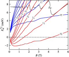
Modulation doped Cd1-xMnxTe semiconductor quantum wells (QWs) possess a very large electronic Lande-factor, which depends on the magnetization of the Mn ions via the s-d exchange interaction Furdyna (1988). In consequence, Landau levels (LLs) with spin up and spin down energies and cross at certain values of the magnetic field, as shown in Fig. 1. The most prominent transition to the QHFM state occurs when the condition is fulfilled for energy which coincides with the chemical potential.
If carrier density corresponds to a filling factor of , electrons are tuned by the magnetic field from the polarized (ferromagnetic) to an unpolarized spin configuration. As a result, a phase transition driven by electron-electron (e-e) exchange interaction, occurs at some critical field Giuliani and Quinn (1985). The new QHFM phase is characterized by a non-uniform texture of spin polarization because the electron liquid is spontaneously divided into 2D ferromagnetic and antiferromagnetic domains Jungwirth and MacDonald (2001). Experimentally, the crossing point of the LLs manifests itself as an additional and rather narrow resistance peak (or a conductance peak). This was indeed observed for diluted magnetic Cd(Mn)Te quantum wells by Jaroszyński et.al. Jaroszyński et al. (2002). Moreover, the shape of the curve around was dependent on the sweep direction of magnetic field. It is widely accepted, that such hysteretic behavior proves the existence of magnetic domains. Electron transport then occurs through a conducting network of randomly connected domain walls Jungwirth and MacDonald (2001); Jaroszyński et al. (2002).
The quantum Hall ferromagnet state for integer filling factors was observed for the first time in non-magnetic semiconductors Koch et al. (1993) and since then it has been extensively studied Chokomakoua et al. (2004), also for the fractional quantum Hall effect regime Smet et al. (2001). Recent renewed interest in the QHFM transition, in particular for diluted magnetic materials, stems from the observation that domain walls that form a percolation path are in fact helical 1D channels. These have potential application to generate non-Abelian excitations Kazakov et al. (2017).
III Interacting chiral channels
When describing the QHFM ground state which is formed at integer in macroscopic samples, attention is usually focused on the bulk properties of the magnetic phases, and it is emphasized that spin splitting is enhanced when level crossings occur in the vicinity of chemical potential. Here, we would like to examine the consequences of LL crossings which take place below Fermi energy in mesoscopic micro-structures, using the language of Quantum Hall edge currents. In this picture, the bulk filling factor decreases in a step-wise manner towards the edge of a device and reaches zero at the physical boundary of the 2DEG system Chklovskii et al. (1992). As a consequence, for a structure made of Cd1-xMnxTe QW, we expect a series of quasi-one-dimensional QHFM transitions to occur along the edges. They may be detectable by non-local measurements of the magnetoconductance.
As a first step towards the verification of these ideas, we calculated with the addition of a term that accounts for the electron-electron interactions. Such a correction is necessary because correlation effects in Cd1-xMnxTe are stronger than e.g. in the well known case of GaAs. Indeed, it has been shown experimentally for a 2D electron gas confined in a CdTe QW that a considerable enhancement of the spin gap occurs for fully occupied LLs below the Fermi energy . Moreover, it has been argued that such enhancement is driven by the total spin polarization and results in a rigid shift of the LL ladders with opposite spins Kunc et al. (2010). Using this assumption, magnetoluminescence and magnetotransport measurements can be successfully described using the following simple formula for a total spin splitting:
| (1) |
It is common for all Landau levels. Here is the spin polarization and is an effective Lande factor of the electrons. Phenomenological constants and have been determined as fitting parameters Kunc et al. (2010).
Following Kunc et al. (2015), we have assumed that those findings apply also for Cd1-xMnxTe quantum wells. Accordingly, we have calculated in a self-consistent way, taking into account the fact that depends on polarization , which in turn depends on the total spin splitting, as it follows from Eq. 1. For the effective -factor in diluted magnetic materials we used a standard formula Furdyna (1988). We assumed that electron density is fixed (see below) and the Mn content was treated as a fitting parameter. We obtained . Results for and temperature are shown in Figs 1 and 2.
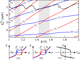
In the language of non-interacting edge currents, such crossing of energy levels corresponds to the situation when two channels, belonging to distinct Landau states and carrying electrons with opposite spins, overlap in real space. This picture is, however, too simplified since correlation effects lift the spatial degeneracy of chiral channels, as explained before. Such reconstruction of spin-split edge channels is schematically illustrated in Fig 2a,b for a quantum structure made from a Cd1-xMnxTe material. Note that the distance between chiral states changes sign as a function of perpendicular magnetic field. Therefore, during such reordering, channels must overlap at critical field, in spite of the reconstruction effect. In fact, Rijkes and Bauer Rijkels and Bauer (1994) showed that demonstrates jumps and bistable behavior dependent on source-drain voltage in the non-linear transport regime (see Fig. 2c).
IV Experiment and results
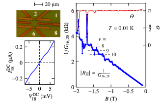
To experimentally test these theoretical predictions we have performed low-temperature magneto-transport measurements on a quasi-ballistic micro-structure produced from a -nm-wide Cd1-xMnxTe QW with a manganese content of . The 2DEG structure was grown by molecular beam epitaxy (MBE) with Cd1-uMguTe barriers (), and modulation doped with iodine donors which were introduced into the top barrier at a distance of from the QW in the growth direction. The 6-terminal microstructure shown in the inset of Fig. 3 was patterned on this substrate using e-beam lithography and deep-etching techniques. The sample was formed into a H-shaped device with an overall size of , connected to the external contacts by 4 multimode wires of the same length () and of geometrical width , which was slightly different for adjacent channels. In particular, and for wires 1 and 8, respectively (see Fig. 3). Additionally, two much shorter and slightly narrower constrictions of were connected to the inner part of the device (terminals 2 and 6).
Special attention was devoted to the fabrication of macroscopic contacts to our device. Typically, electrical connections to Cd(Mn)Te quantum wells are obtained with macroscopic indium droplets, which are burnt-in or soldered locally at the edges of a sample. Such procedures are not fully reproducible and clearly, they are not compatible with e-beam lithography. Nevertheless, they are widely adopted, because the global annealing at temperatures above is not recommended for II-VI materials. In this work, we prepared the soldering pads lithographically, using mercury telluride (HgTe) zero-gap semiconductor as a low-resistivity contact material Jaroszyński et al. (1983). The lowest resistances were obtained when HgTe was thermally evaporated on substrates cooled with liquid nitrogen, in this case the polycrystalline contact material was almost perfectly stoichiometric. After evaporation, the HgTe surface was covered with Cr/Au metal layer and heated locally during the subsequent process of soldering of indium droplets. Contact pads extended to the edges of the device and local annealing occurred far away from the central region of the microstructure. Contacts possessed linear - characteristics with the zero-bias resistances to (for ) and were highly reproducible during the thermal cycling. An example of the - curve, for two contacts connected in series, is shown in Fig. 3.
We studied the local and non-local differential magnetoconductances as a function of DC source-drain voltage , and magnetic field up to 6 T. We employed low-frequency lock-in technique with AC excitation voltage , which was reduced by the finite contact resistances to less then on the sample itself. One of the current contacts, labelled with (), was always connected to virtual ground via the low-noise trans-impedance amplifier *[Experimentalsetupwassimilartothatdescribedin][seealso]Kretinin2011; *Kretinin2012. Conductance is defined here as AC current divided by AC voltage amplitude , measured on () terminals 111AC voltage amplitude was obtained as , where and were real and imaginary parts of measured signal, AC current was driven at reference frequency .. Each collected data point was an average over several read-outs performed at constant magnetic field. The relative phase of and low-frequency signals was also simultaneously recorded. Measurements were carried out in the cryo-free dilution refrigerator Triton 400 at base temperatures ranging from to , and performed in the dark with no illumination.
The electron density , which we used for calculations, has been determined from the quasi-Hall configuration explained in Fig 3. Knowing , we have also estimated the carrier mobility and electron mean free path for our sample. Fig 3 shows Hall resistance vs magnetic field , where the quantized plateaus are observed for filling factors and . The number of occupied LLs and the magnetic field values, for which steps occur, agrees well with the results of calculations, displayed in Figs 1 and 2. However, Hall quantization is not perfect and it entirely disappears for .
Figure 3 also shows the relative phase of Hall voltage as a function of magnetic field. In principle, depends on and frequency via external capacitances of a particular experimental setup. For four-terminal Hall measurements the change of phase is given by , where is the capacitance of a single connecting cable Hernández et al. (2014). In our experimental conditions , as measured at , therefore for . Such a small value is negligible and indeed, does not change monotonically with but on an average remains equal to , as it is expected for , because Hall voltage is negative for 222A small increase of for is observed because the (-) characteristics of electrical contacts were non-linear for ..
However, phase is not constant as a function of magnetic field. We observed a rapid fluctuations of phase signal, which amplitude became very large for . We attribute this effect to the consecutive appearance and disappearance of internal capacitances, induced by magnetic field and related to the formation of edge currents in the specific geometry of our microstructure. It is explained below by analyzing conductance, rather than resistance data.
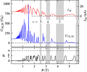
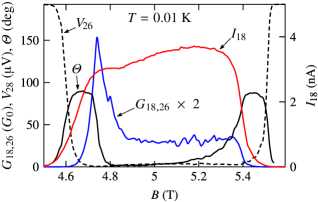
For analysis, we chose a symmetric, quasi-local configuration, in which the wider wires (1) and (8) were used as current contacts and the narrower constrictions (2) and (6) played the role of voltage probes. Figure 4 shows the differential magnetoconductance obtained at together with the AC current , measured simultaneously. For we observed very well resolved Shubnikov-de Haas (SdH) oscillations with a characteristic beating pattern caused by giant spin splitting Kunc et al. (2015). For higher fields, less regular but very pronounced conductance resonances are visible, which are also related to the position of the Fermi level, as explained below. For example, the last resonance appears when approaches energy and filling factor changes from to .
Furthermore, for we recognize regions where current comes close to zero, for example at . At the same time, voltage increases, approaching rms amplitude of the external excitation . Such zero conductance regions are indicated in Fig. 4 with the greyed background. The comparison with Fig. 1 reveals, that those broad conductance anti-resonances correspond to the situation when Fermi energy is located between Landau levels.
A strong anti-resonances of conductance (sometimes called resistance overshoots) were predicted for non-interacting disordered quantum wires Masek et al. (1989) and observed experimentally in GaAs/AlGaAs two-terminal devices Wróbel et al. (1995); *[seealso]Wrobel1996 and narrow Hall-bar structures Kendirlik et al. (2013). They appear, when the central compressible strip of electron liquid in conducting channel is localized by disorder and provides a route for the backscattering. Here, however, the anti-resonances are rather wide and occur when there is no compressible liquid in the central part of the device. Therefore, the filling factor in terminals must differ considerably from its bulk value, to explain the observed current drop. While it is still possible, a large width of the anti-resonances and a very low value of current at the minima rather suggest, that the edge states are at high magnetic fields decoupled from the macroscopic contacts, when enters the energy gap of bulk states.
As already mentioned, HgTe/Cr/Au contact pads were evaporated at the boundaries of the sample, however, they were annealed only locally, during indium soldering. Moreover, polycrystals of HgTe do not form a continuous conducting layer, because of their size (). Therefore, it is very probable that HgTe contacts were well connected to the inner part of the sample but only weakly to the edge. It is known, that such interior contacts are connected to the edge currents through Corbino geometry and therefore the coupling is strongest for the innermost (i.e. farthest from the edge) channel Faist et al. (1991); Haug (1993). Moreover, quantized resistance plateaus are not observed for Corbino samples, instead, the conductance drops to zero for integer filling factors Kobayakawa et al. (2013). Clearly, it is also observed for our device. Therefore we conclude, that HgTe/Cr/Au metal pads form the (unintentionally) interior contacts, which are periodically decoupled from the edge states as a function of magnetic field.
V Disconnected edge currents
While macroscopic interior terminals equilibrate rather with the innermost channels, microscopic quantum point contacts behave in the opposite way, providing coupling to the outermost (i.e. closest to the edges) currents Alphenaar et al. (1990). Below, we argue that this difference determines the relative phase of voltage signal, shown in Fig. 4. The phase does not change much up to , in spite of strong oscillations, whereas for higher fields it switches between and values. Fig. 5 provides a detailed comparison of all measured signals for the to transition region, where chemical potential stays close to the Landau level.
For we observe the conductance maximum, which is even stronger at , when reaches extremely high value of . Vanishing resistance shows that at resonance the outermost edge channel is strongly coupled with both macroscopic and microscopic contacts. In such circumstances, the equilibration between terminals (2) and (6) occurs () and the strong peak of conductance is indeed observed (). For higher fields, Fermi level stays close to LL and sample interior becomes divided into magnetic and non-magnetic domains. The irregular peaks of conductance, observed for still higher fields, are most probably related to the interference pattern of electron waves travelling along a network formed by magnetic domain walls. That picture is supported by the hysteretic behavior of these conductance fluctuations.
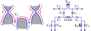
For lower fields () current starts to decrease, because coupling of the outermost edge channels with the interior contacts is weakened. At the same time, the inner edge channel, which is still coupled with macroscopic terminals, does not enter the narrower constrictions, as shown schematically in Fig. 6. Therefore, the inner edge channel is disconnected by microscopic contacts, however, it is still capacitively coupled with the central part of the device by geometrical and/or electrochemical capacitance Christen and Büttiker (1996). Such internal coupling schemes have been investigated experimentally in the kHz Hartland et al. (1995); Hernández et al. (2014) and GHz Gabelli et al. (2006); Hashisaka et al. (2012) frequency ranges. In our case, the appearance of the internal capacitance leads to a phase shift , which for low frequencies approaches the ‘quantized’ value . This conclusion was confirmed by the analysis of a simplified equivalent circuit shown in Fig. 6. We applied Kirchhoff’s laws only to the innermost channels (shown in red). The fully transmitted outermost channel (shown in blue) were not included in the equivalent circuit, because they mutually equilibrate and do not contribute to the measured values of . For simplicity our model ignores the inter-channel scattering, which may occur in the current terminals 333The calculations were performed using QUCS Studio circuit simulator http://dd6um.darc.de/QucsStudio/qucsstudio.html.
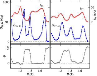
We apply our analysis also to lower magnetic fields () where disorder is reduced by screening and edge channels are not completely decoupled from the macroscopic (interior) contacts. If the phase of voltage signal is determined by the position of Fermi energy alone, as explained above, then pattern will be only weakly dependent on the resistive loads and contact capacitances. It is indeed the case, as it follows from Fig. 7, were results for () and () configurations are shown. In both cases narrow contact (2) plays a role of the current terminal, therefore fluctuates more strongly and on an average is smaller as compared to corresponding () data. Nevertheless, the main features of pattern are very similar for all configurations. Phase approaches value when is close to () Landau level, as if follows from Figs 1 and 2.
Interestingly, phase shift of even lower frequency () signal have been observed during the measurements of longitudinal resistance in the QHE regime at filling factor for a standard macroscopic Hall-bar device Desrat et al. (2000). Authors attributed the existence of a zero frequency phase shift to a predominantly inductive load *[Seealsodiscussionin][]Melcher2001. For simplicity, our model ignores the inductance like contributions to admittance Christen and Büttiker (1996). In any case, however, a small phase shift () guarantees that edge channels are resistively coupled to contact areas.
VI Local QHFM transition
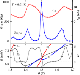
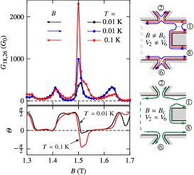
In the following, we concentrate on the local QHFM transition, which corresponds to the pronounced conductance maximum of (in units) observed at . Figure 8 shows an enlarged view of three adjacent conductance resonances, occurring at . We attribute central peak to the crossing of the and Landau levels, as shown in the energy diagram of the lower panel. For this, the relative energies of spin-down and spin-up states together with the position of the Fermi level were calculated self-consistently with Mn content taken as the only fitting parameter. We obtained , which is in reasonable agreement with other features observed for the whole range of magnetic fields, as discussed above. The lower panel shows also the relative phase of voltage signal vs magnetic field for this configuration. According to the previous discussion, when Fermi energy is located between Landau levels and approaches value when is close to one of the quantized energy states. We would like to stress, that for the central conductance peak and then changes abruptly when Landau levels and alter their positions. At the same time, current (i.e. load resistance) practically does not change over the resonance width.
The properties of the central conductance peak, observed for local () configuration, are further examined in Fig 9. The middle resonance is higher and narrower than its neighbors. Moreover, it shows hysteretic behavior together with a strong and unusual temperature dependence. At conductance increases and reaches value. Note also, that at resonance we still have , however, the off-resonance phase changes more abruptly towards value as compared to data obtained at .
We deduce that the shape of resonance at , which is much narrower than neighboring maxima, is a direct consequence of degenerate edge channel reconstruction. This is explained in the right part of Fig. 9, where the upper drawing shows a schematic of our device for . Near the resonance, non-interacting edge currents should lie very close to each other. However, Coulomb repulsion pushes the state away from the edge (and away from state ) by a distance of approximately . Consequently, there is a non-zero probability that outermost channel emanated from contact (8) is back-scattered at the entrance contact (1), which is narrower. As a result, equilibration among edge currents which were initially in balance with different current contacts occurs. Due to scattering, which is marked with dotted lines in the figure, probe (2) in not in equilibrium with contact (1) and there is a considerable phase shift between the voltage and current signals. The same picture applies equally well for , the only difference being that abruptly changes sign. This explains why conductance resonances related to level crossings are very narrow. To understand the situation at resonance, suppose that at the edge currents can overlap () as illustrated schematically in the the lower-right part of Fig. 9. Then, the degenerate channel is closer to the edge and back-scattering caused by differences of width and by disorder is considerably weaker. In the ideal situation, probe (2) is in equilibrium with contact (1) and probe (6) is balanced with probe (2). Therefore, and differential conductance is very large with a small current-voltage phase shift . This picture is in agreement with experimental results and explains the large amplitude of resonances associated with the local QHFM transitions.
As already mentioned, at the conductance peak is higher than at lower temperatures, though it is difficult to find systematic trends because of hysteretic behavior. In particular, some maxima are different whether magnetic field is raised or lowered as seen in Fig. 9. For sharp resonances, this is apparently related to the presence of a narrow hysteresis loop, similar to that shown in Fig. 2c with replaced by . Freire and Egues Freire and Egues (2007) predicted such hysteresis for Cd(Mn)Te materials when electron density is globally tuned to the QHFM transition. In our opinion such a mechanism can also operate locally for any carrier concentration, since LLs coincide with the chemical potential at the sample edge. Therefore, the observed hysteresis may be related to the a metastable channel reconstruction, but also to the pinning of 1D magnetic domains which are formed when changes sign along the boundaries. Such effects may be a source of non-linearity in quantum transport and indeed, the Onsager relations are fulfilled only approximately for conductance resonances, see Fig. 7.
VII Crossing of edge currents
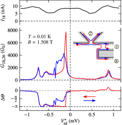
Rijkels and Bauer Rijkels and Bauer (1994) suggested that such a change of sign can be created on demand when spatially separated edge currents are brought out of equilibrium. Then, the edge states cross at certain points giving rise to the formation of magnetic domain walls. Those authors also pointed out that a chemical potential difference can be most easily created by the introduction of a spin selective barrier across one of the current contacts. Such circumstances are naturally realized in our sample, since the wire contact (1) is about narrower than the second current terminal (8) – see the top-right schematic in Fig. 9. Therefore, a non-equilibrium population of outermost edge currents was accomplished by applying a source-drain voltage difference on contacts (1) and (8).
The experiment was conducted as follows. We again focused on the conductance maximum at and the magnetic field value was fixed at in order to slightly detune from the resonance peak. This corresponds to the situation shown schematically in Fig. 2b for , where the separation distance of edge currents is . By applying a source-drain voltage one hopes to reduce the absolute value of separation, tune back to the resonance and eventually force the edge channels to cross. See Fig. 2c.
The results are summarized in Fig. 10, where upper panel shows as a function of the chemical potential difference between contacts (1) and (8), denoted as . Let us focus on the red line. For negative values of , we observe a very high and narrow conductance peak at having a half-width of . It is very similar to the resonances obtained as a function of magnetic field. As explained before, a maximal conductance corresponds to a minimal distance between edge currents. Therefore, further increase of should induce channel swapping and a decrease of conductance.
This is indeed what was observed in the experiment. The lower panel shows , the change of the AC voltage phase relative to its value at . This phase changes abruptly by 180 degrees just after passing the resonance, as would be expected when edge currents cross at some point and interchange their positions. In our case, the voltage probe (2) is in equilibrium with the current contact (8) when the intersection is created and the phase of the signal is shifted by . See the inset of Fig. 10, keeping in mind that not only one (as shown) but also an odd number of crossings located between probes, will lead to . Interestingly, is close to down to , suggesting that channels are still connected to reservoirs. Note also, that (-) curve is almost exactly symmetrical around zero as it is evident from data presented in the upper panel. Therefore, the abrupt phase change must be attributed to channel reordering.
As pointed out by Rijkels and Bauer, each crossing point causes the topological problem of how to connect edge channels to the macroscopic terminals, which in equilibrium emanate states with a normal ordering of spins. Therefore, the channels have to switch again somewhere, and one of such possible crossings is shown in the inset on the left of probe (2), two others on the other side. The number of topological defects depends on mutual electrostatic repulsion Rijkels and Bauer (1994) and our data suggest that the constriction itself (which plays a role of voltage probe) may induce a channel switch. In that case, channel ordering is reversed in the vicinity of a smooth saddle-point potential, as compared to the outer regions of a constriction. Quite recently it was suggested that for low Zeeman energies the ordering of the edge modes switches abruptly at the narrowing, while the arrangement in wider areas remains intact Khanna et al. (2017). Such mechanism, driven by spin exchange interaction may operate here.
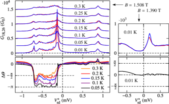
Figure 10 also shows results obtained when the source-drain voltage was increased from negative to positive values. For conductance reveals strong instabilities and deviates from . It appears that the system was trapped in a metastable state for which channel coupling to reservoirs is different. However, the hysteretic behavior shown in Fig. 10 represents a rather extreme case. Typically, conductance instabilities are weaker, as illustrated in the left part of Fig 11 where and for data are shown. Analogous data for the neighboring conductance peak (see Fig 9), recorded at , are shown to the right. Also here, we can tune back to the resonance with source-drain voltage (this time for ), however, the phase of the voltage signal practically does not change when conductance passes through its maximum. This proves that the abrupt change of by is characteristic for LLs crossings only.
Data for channel crossing at are also shown as a function of temperature. For the fluctuations of the peak value are smaller and the conductance resonance gradually disappears. However, at it is still clearly visible. A strong temperature dependence of is also observed for the range of source-drain voltages that corresponds to a channel crossing. At , the phase changes when detuned off-resonance by almost exactly 180 degrees, but at higher temperatures it is continuously reduced, reaching about 90 degrees seen at . Such temperature averaging of phase (over the extreme values of and ) happens when is of the order of , the energy difference between spin-up and spin-down electrons at the edge of a sample. For , the temperature dependence of and is much weaker, which is expected since increases and channel crossing does not occur.
All this fits very well to the picture of edge current reconstruction and local channel crossing predicted by theory. There are, however, some noticeable differences. First, the almost symmetrical hysteresis shown schematically in Fig 2c occurs only for negative values of source-drain voltage and therefore in experiment is highly asymmetric. Second, the bistability predicted by Rijkels and Bauer does not manifest itself clearly, because abrupt changes of from to 0 are not observed. Finally, is much smaller than calculated by theory Dempsey et al. (1993); Rijkels and Bauer (1994). However, it is known that the splitting is overestimated in the Hartree-Fock approximation and in our case spin levels belong to different orbitals, therefore exchange effects are strongly reduced. On the other hand, the anticrossing gap between the edge channels may be enhanced by spin-orbit coupling as suggested previously for bulk states in Kazakov et al. (2016). There, was obtained for the and Landau levels.
In fact, our experiment covers a broader range of phenomena than have been considered by the theories discussed above. In the non-linear transport regime we observed two additional conductance maxima, on both sides of the central resonance peak, as clearly visible in Figs 10 and 11. We attribute them to the crossings of Landau levels, which are adjacent in energy and gradually appear in a conductance window when source-drain voltage is applied. The left resonance appears to be related to an intersection of the states and , located below the Fermi level in equilibrium. Apart from a smaller amplitude this peak is very similar to the central resonance with regard to temperature dependence, fluctuations of the maximal value. Most importantly, it is also connected with a change of the AC voltage signal phase by 180 degrees. The right resonance is most probably related to the intersection of the and states, which are not occupied for . In this case, the observed phase changes and temperature dependence of conductance are much weaker.
VIII Summary
In summary, we have presented the results of low temperature magneto-transport measurements, obtained using a low-frequency lock-in technique. Measurements were carried out on a quasi-ballistic micro-structure created on a very good quality type Cd1-xMnxTe diluted magnetic quantum well. We analysed not only amplitude of conductance , but also phase of the measured signal. We have observed sudden jumps of phase between and values, which we explained as a consecutive coupling and decoupling of the inner edge channels to the current and voltage contact areas. Most importantly, for (and ) we have observed high and narrow conductance resonance attributed to transition to the QHFM phase, which occurs at sample boundary and is accompanied by the reconstruction of spin-degenerate edge states. Furthermore, we show that a local crossing or reordering of spatially separated chiral channels, which is associated with the change of by , can be induced on demand by applying a DC source-drain voltage.
Acknowledgements.
The research was partially supported by the National Science Centre (Poland) through grants No. DEC- 2012/06/A/ST3/00247, 2016/23/N/ST3/03500 and by the Foundation for Polish Science through the IRA Programme co-financed by the EU within SG OP. Authors wish to thank P. Deuar and T. Dietl for valuable remarks.References
- Dempsey et al. (1993) J. Dempsey, B. Y. Gelfand, and B. I. Halperin, Phys. Rev. Lett. 70, 3639 (1993).
- Chklovskii et al. (1992) D. B. Chklovskii, B. I. Shklovskii, and L. I. Glazman, Phys. Rev. B 46, 4026 (1992).
- Meir (1994) Y. Meir, Phys. Rev. Lett. 72, 2624 (1994).
- Wang et al. (2017) J. Wang, Y. Meir, and Y. Gefen, Phys. Rev. Lett. 118, 046801 (2017).
- Klein et al. (1995) O. Klein, C. de C. Chamon, D. Tang, D. M. Abusch-Magder, U. Meirav, X. G. Wen, M. A. Kastner, and S. J. Wind, Phys. Rev. Lett. 74, 785 (1995).
- Sabo et al. (2017) R. Sabo, I. Gurman, A. Rosenblatt, F. Lafont, D. Banitt, J. Park, M. Heiblum, Y. Gefen, V. Umansky, and D. Mahalu, Nature Physics 13, 491 (2017).
- Rijkels and Bauer (1994) L. Rijkels and G. E. W. Bauer, Phys. Rev. B 50, 8629 (1994).
- Bocquillon et al. (2013) E. Bocquillon, V. Freulon, J.-. M. Berroir, P. Degiovanni, B. Plaçais, A. Cavanna, Y. Jin, and G. Fève, 4, 1839 (2013).
- Fève et al. (2007) G. Fève, A. Mahé, J.-M. Berroir, T. Kontos, B. Plaçais, D. C. Glattli, A. Cavanna, B. Etienne, and Y. Jin, Science 316, 1169 (2007).
- Deviatov et al. (2005) E. V. Deviatov, V. T. Dolgopolov, A. Würtz, A. Lorke, A. Wixforth, W. Wegscheider, K. L. Campman, and A. C. Gossard, Phys. Rev. B 72, 041305 (2005).
- Furdyna (1988) J. K. Furdyna, Journal of Applied Physics 64, R29 (1988), https://doi.org/10.1063/1.341700 .
- Giuliani and Quinn (1985) G. F. Giuliani and J. J. Quinn, Phys. Rev. B 31, 6228 (1985).
- Jungwirth and MacDonald (2001) T. Jungwirth and A. H. MacDonald, Phys. Rev. Lett. 87, 216801 (2001).
- Jaroszyński et al. (2002) J. Jaroszyński, T. Andrearczyk, G. Karczewski, J. Wróbel, T. Wojtowicz, E. Papis, E. Kamińska, A. Piotrowska, D. Popović, and T. Dietl, Phys. Rev. Lett. 89, 266802 (2002).
- Kunc et al. (2015) J. Kunc, B. A. Piot, D. K. Maude, M. Potemski, R. Grill, C. Betthausen, D. Weiss, V. Kolkovsky, G. Karczewski, and T. Wojtowicz, Phys. Rev. B 92, 085304 (2015).
- Koch et al. (1993) S. Koch, R. J. Haug, K. v. Klitzing, and M. Razeghi, Phys. Rev. B 47, 4048 (1993).
- Chokomakoua et al. (2004) J. C. Chokomakoua, N. Goel, S. J. Chung, M. B. Santos, J. L. Hicks, M. B. Johnson, and S. Q. Murphy, Phys. Rev. B 69, 235315 (2004).
- Smet et al. (2001) J. H. Smet, R. A. Deutschmann, W. Wegscheider, G. Abstreiter, and K. von Klitzing, Phys. Rev. Lett. 86, 2412 (2001).
- Kazakov et al. (2017) A. Kazakov, G. Simion, Y. Lyanda-Geller, V. Kolkovsky, Z. Adamus, G. Karczewski, T. Wojtowicz, and L. P. Rokhinson, Phys. Rev. Lett. 119, 046803 (2017).
- Kunc et al. (2010) J. Kunc, K. Kowalik, F. J. Teran, P. Plochocka, B. A. Piot, D. K. Maude, M. Potemski, V. Kolkovsky, G. Karczewski, and T. Wojtowicz, Phys. Rev. B 82, 115438 (2010).
- Jaroszyński et al. (1983) J. Jaroszyński, T. Dietl, M. Sawicki, and J. Elżbieta, Physica B+C 117-118, 473 (1983).
- Kretinin et al. (2011) A. V. Kretinin, H. Shtrikman, D. Goldhaber-Gordon, M. Hanl, A. Weichselbaum, J. von Delft, T. Costi, and D. Mahalu, Phys. Rev. B 84, 245316 (2011).
- Kretinin and Chung (2012) A. V. Kretinin and Y. Chung, Review of Scientific Instruments 83, 084704 (2012), https://doi.org/10.1063/1.4740521 .
- Note (1) AC voltage amplitude was obtained as , where and were real and imaginary parts of measured signal, AC current was driven at reference frequency .
- Hernández et al. (2014) C. Hernández, C. Consejo, P. Degiovanni, and C. Chaubet, Journal of Applied Physics 115, 123710 (2014), https://doi.org/10.1063/1.4869796 .
- Note (2) A small increase of for is observed because the (-) characteristics of electrical contacts were non-linear for .
- Masek et al. (1989) J. Masek, P. Lipavsky, and B. Kramer, Journal of Physics: Condensed Matter 1, 6395 (1989).
- Wróbel et al. (1995) J. Wróbel, T. Brandes, F. Kuchar, B. Kramer, K. Ismail, K. Y. Lee, H. Hillmer, W. Schlapp, and T. Dietl, EPL (Europhysics Letters) 29, 481 (1995).
- Wróbel (1996) J. Wróbel, Acta Physica Polonica A 90, 691 (1996).
- Kendirlik et al. (2013) E. M. Kendirlik, S. Sirt, S. B. Kalkan, W. Dietsche, W. Wegscheider, S. Ludwig, and A. Siddiki, Scientific Reports 3, 3133 (2013).
- Faist et al. (1991) J. Faist, P. Guéret, and H. P. Meier, Phys. Rev. B 43, 9332 (1991).
- Haug (1993) R. J. Haug, Semiconductor Science and Technology 8, 131 (1993).
- Kobayakawa et al. (2013) S. Kobayakawa, A. Endo, and Y. Iye, Journal of the Physical Society of Japan 82, 053702 (2013), https://doi.org/10.7566/JPSJ.82.053702 .
- Alphenaar et al. (1990) B. W. Alphenaar, P. L. McEuen, R. G. Wheeler, and R. N. Sacks, Phys. Rev. Lett. 64, 677 (1990).
- Christen and Büttiker (1996) T. Christen and M. Büttiker, Phys. Rev. B 53, 2064 (1996).
- Hartland et al. (1995) A. Hartland, B. P. Kibble, P. J. Rodgers, and J. Bohacek, IEEE Transactions on Instrumentation and Measurement 44, 245 (1995).
- Gabelli et al. (2006) J. Gabelli, G. Fève, J.-M. Berroir, B. Plaçais, A. Cavanna, B. Etienne, Y. Jin, and D. C. Glattli, Science 313, 499 (2006), http://science.sciencemag.org/content/313/5786/499.full.pdf .
- Hashisaka et al. (2012) M. Hashisaka, K. Washio, H. Kamata, K. Muraki, and T. Fujisawa, Phys. Rev. B 85, 155424 (2012).
- Note (3) The calculations were performed using QUCS Studio circuit simulator http://dd6um.darc.de/QucsStudio/qucsstudio.html.
- Desrat et al. (2000) W. Desrat, D. K. Maude, L. B. Rigal, M. Potemski, J. C. Portal, L. Eaves, M. Henini, Z. R. Wasilewski, A. Toropov, G. Hill, and M. A. Pate, Phys. Rev. B 62, 12990 (2000).
- Melcher et al. (2001) J. Melcher, J. Schurr, F. Delahaye, and A. Hartland, Phys. Rev. B 64, 127301 (2001).
- Freire and Egues (2007) H. J. P. Freire and J. C. Egues, Phys. Rev. Lett. 99, 026801 (2007).
- Khanna et al. (2017) U. Khanna, G. Murthy, S. Rao, and Y. Gefen, Phys. Rev. Lett. 119, 186804 (2017).
- Kazakov et al. (2016) A. Kazakov, G. Simion, Y. Lyanda-Geller, V. Kolkovsky, Z. Adamus, G. Karczewski, T. Wojtowicz, and L. P. Rokhinson, Phys. Rev. B 94, 075309 (2016).