Crystal-field effects in graphene with interface-induced spin–orbit coupling
Abstract
We consider theoretically the influence of crystalline fields on the electronic structure of graphene placed on a layered material with reduced symmetry and large spin–orbit coupling (SOC). We use a perturbative procedure combined with the Slater-Koster method to derive the low-energy effective Hamiltonian around the points and estimate the magnitude of the effective couplings. Two simple models for the envisaged graphene–substrate hybrid bilayer are considered, in which the relevant atomic orbitals hybridize with either top or hollow sites of the graphene honeycomb lattice. In both cases, the interlayer coupling to a crystal-field-split substrate is found to generate highly anisotropic proximity spin–orbit interactions, including in-plane ’spin–valley’ coupling. Interestingly, when an anisotropic intrinsic-type SOC becomes sizeable, the bilayer system is effectively a quantum spin Hall insulator characterized by in-plane helical edge states robust against Bychkov-Rashba effect. Finally, we discuss the type of substrate required to achieve anisotropic proximity-induced SOC and suggest possible candidates to further explore crystal field effects in graphene-based heterostructures.
I Introduction
The impact of the crystal environment on atomic states is pivotal to understand the electronic structure of solids containing transition metal atoms FazekasBook . For instance, in high-Tc cuprates, crystal field states are essential in the description of planes, where ions are surrounded by elongated octahedral structures of O atoms Dagotto1994 ; ZhangRice1988 . Crystal electric field effect and its interplay with spin–orbit coupling plays an important role in magnetic anisotropy Sati2006 ; Sachidanandam97 Jahn-Teller effect Jahn1936 ; Ishihara97 ; Salamon2001 , distortive order Ishizuka1996 and cooperative Jahn-Teller effect Gehring1975 .
More recently, it has been appreciated that crystal field effect (CFE) underlies rich spin-dependent phenomena at metallic interfaces. For instance, the broken rotational symmetry of magnetic atoms in metal bilayers was found to render spin currents anisotropic Cahaya2017 , while a staggered CFE associated to nonsymmorphic structures of metal species is responsible for a giant enhancement of Rashba effect in BaNiS2 Cottin16 . Here, we investigate the electronic properties of graphene placed on nonmagnetic substrates characterized by a sizable CFE. Graphene–substrate hybrid bilayers are currently attracting enormous interest due to the combination of Dirac fermions and prominent interfacial spin–orbital effects in the atomically-thin (two-dimensional) limit Song2010 ; Lee2015 ; Rajput16 . Monolayers of group VI transition metal dichalcogenides (TMDs) are a particularly suitable match to graphene as a high SOC substrate. The peculiar spin–valley coupling in the TMD electronic structure Xiao_TMD ; Wang_TMD_12 ; Mak_TMD_16 provides a unique all-optical methods for injection of spin currents across graphene–TMD interfaces Muniz_Sipe_15 ; Fabian2015 , as recently demonstrated AvsarOzyilmaz2017 ; Luo_17 . Furthermore, the proximity coupling of graphene to a TMD base breaks the sublattice symmetry of pristine graphene leading to competing spin–valley and Bychkov-Rashba spin–orbit interactions Avsar2014 ; WangMorpurgo2015 ; Whang2017 ; Zihlmann2018 ; Cummings2017 ; vanWees2017 ; velenzuelaNat2017 ; OmarVanWees2018 . The enhanced SOC paves the way to bona fide relativistic transport phenomena in systems of two-dimensional Dirac fermions, including the inverse spin galvanic effect Milletari2017 ; Offidani2017 .
On a qualitative level, the band structure of graphene weakly coupled to a high SOC substrate can be understood from symmetry. The intrinsic spin–orbit coupling (SOC) of graphene is invariant under the full symmetries of the point group , which includes 6-fold rotations and mirror inversion about the plane KaneMele1 . The reduction of the full point group in heterostructures is associated with the emergence of other interactions Pachoud2014 ; Kochan_17 . For example, interfacial breaking of inversion symmetry reduces the point group , allowing finite (non-zero) Bychkov-Rashba SOC Rashba2009 . The low-energy Hamiltonian compatible with time-reversal symmetry is
| (1) | |||||
where is the Fermi velocity of massless Dirac fermions, is the wavevector around a Dirac point (valley), and and are Pauli matrices acting on valley, sublattice, and spin spaces, respectively. Here, () are the energy scales of the intrinsic-type SOC (Bychkov-Rashba) interaction enhanced by the proximity effect.
In addition, the interaction of graphene with an atomically flat substrate renders the two carbon sublattices inequivalent, further reducing the point group . A well-studied example is graphene on semiconducting TMD monolayers in the group-IV family. The hybridization between -electrons and the TMD orbitals generates a spin–valley term in the continuum model, reflecting the generally different effective SOC on and sublattices WangMorpurgo2015 ; MGmitra2016 . The breaking of sublattice symmetry also generates a mass term (of orbital origin), which can exceed tens meV in rotationally-aligned van der Waals heterostructures Hunt_14 ; Jung_15 . Another example of reduced symmetry occurs in graphene with intercalated Pb nano-islands Calleja2015 , where a rectangular superlattice potential leads to an in-plane spin–valley coupling in Eq. (1). Finally, if time-reversal symmetry is broken, e.g., using a ferromagnetic substrate, a number of other spin–orbit terms are generally allowed Phong_17 .
Below, we show that the above picture is further enriched when -electrons in graphene experience a crystal field environment via hybridization to crystal-split states. The interlayer coupling to a low-symmetry substrate removes the rotational invariance from the effective Hamiltonian Eq. (1), leading to a proliferation of spin–orbit interactions, including in-plane spin–valley () and anisotropic intrinsic-type () SOC. To estimate the strength of the proximity spin–orbit interactions, we consider a minimal tight-binding model for a hybrid bilayer with hopping parameters obtained from the Slater–Koster method SlaterKoster ; Harrison . We present explicit calculations for two idealized substrates, in which a commensurate monolayer of heavy atoms sit at hollow and top sites of pristine graphene. Finally, a Löwdin perturbation scheme is employed to obtain the low-energy continuum Hamiltonian. As a concrete example, we then discuss the possibility of obtaining an enhanced in-plane spin–valley coupling in a hybrid heterostructure of graphene and a group-IV dichalcogenide monolayer. The article is organized as follows. In Sec. II, we introduce the substrate model and discuss how the eigenstates of free atomic shells are affected by CFE. In Sec. III, we derive the effective Hamiltonian, when the emergent rotational symmetry () is broken by the crystal field environment. In Sec. IV, we address the scenario where, added to CFE, the point group is reduced by a sublattice-dependent interaction with atoms of the substrate, which give rises to new types of SOCs. In Sec. V, we discuss possible realizations with group-IV TMD monolayers. Section VI presents our conclusions.
II Substrate Model
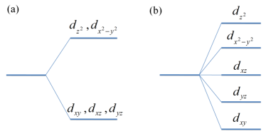
We assume a sufficiently weak interlayer interaction between graphene and the substrate MGmitra2016 ; Phong_17 ; Giovannetti_07 , so that the electronic states near the Fermi level derive mostly from - (graphene) states. Since we are mainly interested in the interplay between CFE and SOC, we shall focus on substrates containing transition metal atoms. We focus on atomic species with outer free shell formed by -states (). The electronic states of a free atom are complex wave functions with well defined angular momentum projection. When an ion is placed in a crystalline environment, its electronic states suffer distortions due to the electric field generated by the surrounding atoms. For () atomic states, this effect is usually stronger than the spin–orbit interaction itself, which can then be treated as a perturbation FazekasBook . The electronic states of a free atom are -fold degenerate (neglecting relativistic corrections), but when the atom is placed in a low-symmetry environment, the degeneracy is lifted [see Fig. 1(a)]. Depending on the crystal symmetry, some of the original complex atomic states combine to form real atomic states with no defined angular momentum projection. If the symmetry is sufficiently low, as in an orthorhombic crystal, the degeneracy is fully lifted [see Fig. 1(b)], and the atomic wavefunctions are real.
The Hamiltonian is written as , where is the standard nearest-neighbor tight-binding Hamiltonian for -electrons in graphene and is the interlayer interaction. To simplify the analysis, hopping processes within , as well as disorder effects, are neglected. Such an approximation suffices for a qualitative description of the effective (long-wavelength) interactions mediated on graphene note_local . Finally, we assume a general low-symmetry environment, such that the atomic Hamiltonian for the external free shell subspace reads as , with
| (2) | |||
| (3) |
where runs over the substrate atoms and () the associated dimensionless orbital (spin) angular momentum operators. The first term [Eq. (2)] describes the crystal field splitting of levels comment_energies . The second term [Eq. (3)] is the spin–orbit interaction on the substrate atoms. We note in passing that CFEs can also lead to anisotropic SOC in Eq. (3) Santos2017 . Such (usually small) anisotropy is neglected here, since its main effect is simply a modulation of the magnitude of the effective SOCs on graphene.
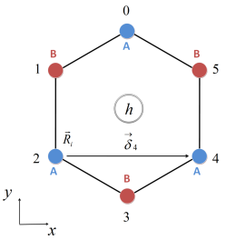
We consider two types of commensurate substrates. In the first type, transition metal atoms of a given species are placed at distance above the center of a hexagonal plaquette in graphene (hollow position in Fig. 2). In the second type, the atoms are located at a distance above a carbon atom (top position). The unit cell of graphene is formed by two sublattices and, as such, there are two possible top configurations: and (see Fig. 3). The eigenstates of the first term Eq. (2) in space representation can be written as
| (4) |
where is the radial part of wave-function, , () are tesseral harmonics. Unlike spherical harmonics (eigenfunctions of ), tesseral harmonics are real functions and do not have spherical symmetry. For calculation purposes, we recast the wavefunctions (we omit the radial part hereafter) in terms of eigenstates of as
| (5) | |||
| (6) | |||
| (7) | |||
| (8) | |||
| (9) |
Below, we show that the main effect of the hybridization of graphene orbitals with non-spherically symmetric states of the substrate is to induce anisotropic SOC.
III Effective Hamiltonian: hollow position
As a simple model for the substrate, we consider a monolayer of heavy atoms sitting at the hollow sites. The -orbitals of each substrate atom hybridize with the states of the nearest six carbon atoms (other hoppings are much smaller and thus are neglected). The hybridization Hamiltonian is , with
| (10) |
where are lattice vectors, is the position of inside the plaquette, for (up) down states and
| (11) |
Here, runs anti-clockwise and follows the convention in Fig. 2 and for even (odd) . The substrate–graphene hopping amplitudes are defined by , where are vectors connecting neighboring carbon atoms ReviewNuno ; see Fig. 2.
The hopping amplitudes are evaluated by means of the Slater–Koster approach SlaterKoster ; Harrison
| (12) | |||
| (13) | |||
| (14) | |||
| (15) | |||
| (16) |
where and are two-centers integrals, which can be obtained by quantum chemistry methods or by fitting to first-principles electronic structure calculations Cappelluti2013 ; SilvaGuillen2016 . are direction cosines of the vector connecting a -carbon atom and the substrate atom at position. The hopping amplitudes are given in the Appendix.
We are interested in the low-energy theory near the Dirac points . The Fourier transform of the hopping matrix at these points can be easily computed and we obtain, for each valley ()
| (17) |
The various constants read as , , and , where , with being the distance between two carbon atoms.
Next, we use degenerate perturbation theory to obtain a graphene-only effective Hamiltonian
| (18) | |||||
where we treated the spin–orbit term of the substrate Hamiltonian as a next-order perturbation compared to . The first term can be expressed in terms of Pauli matrices:
| (19) |
with
| (20) |
The first term in Eq. (19) is a trivial energy shift. The interaction is an orbital term, which can be absorbed by a redefinition of in Eq. (1). The interplay between SOC and CFE is captured by the second term, , which has the form
| (21) | |||||
with couplings determined by
| (22) | |||
| (23) | |||
| (24) | |||
| (25) |
The first two terms in Eq. (21) form an anisotropic Bychkov-Rashba coupling. The third term is the familiar intrinsic-like SOC. The last term is an in-plane spin–valley coupling, leading to an anisotropic spectrum. Note that this term vanishes in the absence of crystal field splitting. The same effective couplings in Eqs. (19) and (21) were obtained in Ref. Calleja2015 for Pb atoms in the absence of CFE due to the reduced point group symmetry of the underlying superlattice.
IV Effective Hamiltonian: Top Position
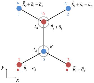
We assume that the top positions ( and ) are occupied by different atomic species (or, equivalently, equal species placed at different distances from graphene). This accounts for the important class of a graphene interface with reduced point group symmetry (in the absence of CFE). Such a sublattice-dependent interaction was absent in the hollow position case. The hybridization between orbitals of graphene and -atoms on top position can be written as , where the hopping matrix is given by
| (26) | |||||
and the -states are defined in similar way to the hollow position case, namely,
| (27) | |||
| (28) |
where and . Similar definitions are employed for states in Eq. (26).
The hopping parameters are written in the Appendix. Around points in the hexagonal Brillouin zone, the hopping matrix can be written as where
| (29) | |||||
with the various constants given in Appendix. Degenerate perturbation theory yields
| (30) | |||||
with coupling constants
| (31) | |||||
| (32) | |||||
representing an energy shift and a staggered sublattice potential, respectively. The combined effect of crystal field and SOC can be written as
| (33) | |||||
where the coupling constants are given by
| (34) | |||
| (35) | |||
| (36) | |||
| (37) | |||
| (38) | |||
| (39) |
In addition to the SOCs already obtained in the hollow case, the combination of a sublattice dependent interaction and CFE gives rise to new terms. We obtain the expected spin–valley coupling , which together with the Bychkov-Rashba SOC are the dominant spin–orbit interactions in group-VI TMD–graphene bilayers WangMorpurgo2015 ; MGmitra2016 . Interestingly, the broken orbital degeneracy in the substrate also generates an in-plane intrinsic spin-orbit coupling . This term can open a quantum spin Hall insulating gap that is robust against Bychkov-Rashba SOC. A more detailed analysis of the effect of this interaction will be given in the next section.
It is instructive to consider two different limiting cases. First we consider the situation where all the energies orbitals of the substrate are degenerate, i.e., absence of a CFE. By analyzing the coupling constants on equations (34-39) the only couplings that remain are the familiar isotropic Bychkov-Rashba coupling, intrinsic-like SOC and the spin–valley term. These same couplings were obtained for TMD/graphene heterostructures WangMorpurgo2015 ; MGmitra2016 and enable interesting spin-dependent phenomena, such as anisotropic spin lifetime Cummings2017 , spin Hall effect Milletari2017 and inverse spin galvanic effect Offidani2017 . The second limit case is when top positions and are equivalent, so that one has , and . For this situation the SOCs that appears are the same of Eq. (21) for hollow position case due to the restoration of sublattice symmetry.
V Discussion
This paper aims to explore the modifications to the electronic states of graphene placed on a substrates characterized by a crystal field environment. In a realistic scenario, we expect the proximity-induced SOC to be sensitive to the type of crystal field splitting and the valence of the substrate atoms. A quantitative analysis is beyond the scope of this work. Nevertheless, the crystal field is expected to be significant in compounds containing transition metals atoms, in which the incomplete outer shell is formed by electrons. The electronic structure of certain TMDs is known to be strongly affected by CFE on the atomic states of transition metal (TM) atoms Gong2013 ; Zhang2015 . TMD layers consist of an hexagonally close-packed sheet of TM atoms sandwiched between sheets of chalcogen atoms and their metal coordination can be either trigonal prismatic or octahedral. In the trigonal prismatic coordination, the two chalcogen sheets are stacked directly above each other (known as H phase). The stacking order in the octahedral phase (T phase) is ABC and the chalcogen atoms of one of the sheets can be located at the center of the honeycomb lattice. In this case, the coordination of the TM atoms is octahedral.
Group IV TMDs have an octahedral structure, whereas group VI TMDs, of the well studied W and Mo compounds, tend to display a trigonal prismatic geometry, whereas both octahedral and trigonal prismatic phases are observed in group V TMDs. The trigonal prismatic geometry enforces a splitting of orbitals in an single state and two doublets and . On the other hand, in the octahedral geometry, a doublet and a triplet are formed. Going back to Eqs. (21) and (33), one can see that the main signatures of the CFE is the broken rotational symmetry in the continuum due to the hybridization of graphene with states without spherical symmetry. The latter results in a in-plane spin–valley coupling, and an anisotropic Bychkov-Rashba SOC. For both top- and hollow- position cases, it is necessary that , for the appearance of the in-plane spin–valley coupling, which is the case of TM atoms with an octahedral distortion; see Fig. 1(a). This type of crystal field is found in the group IV family ( where , and ) and opens up the possibility to observe this coupling in bilayers of these materials and graphene. Less attention has been paid to this family Jiang2011 ; Li2014 compared to group V and VI TMDs. The application of Zr-based chalcogenides in solar energy devices has been suggested Jiang2011 , and the possibility of tuning its properties by pressure, electric field and phase engineering was recently explored in density functional theory calculations Kumar2015 . Our findings suggest that TMDs of family IV are potential candidates to induce non-trivial spin textures in graphene via proximity coupling. On the other hand, the anisotropic Bychkov-Rashba coupling requires , which is only possible in a very low symmetry environment. The low symmetric -phase in WTe2 monolayers, that presents a quantum spin Hall phase Qian2014 ; Wu2018 , could induce an anisotropic Rashba coupling in graphene. This type of anisotropy can lead to an increase of the spin Hall angle in graphene decorated with SOC impurities Cazalilla2016 .
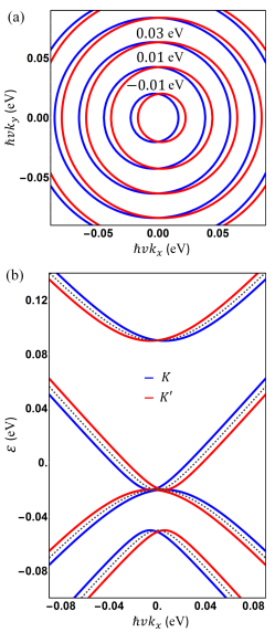
For large interlayer distances, the overlap matrix between states centred on different atomic positions can be neglected, and we can use Eqs. (22)-(25) and (34)-(39) to perform a rough estimative of the different SOCs. Using Slater–Koster parameters for TM-carbon bonds as reported in Ref. Le1991 and the crystal-field splitting and spin–orbit energy () reported in Ref. Jiang2011, , we estimate the graphene effective SOCs for distances times the graphene’s lattice spacing. The dominant SOCs are found to be Kane–Mele and Rashba couplings, with estimated magnitude in the range for both hollow and top substrate atoms, which is consistent with the robust weak antilocalization features in magnetocondutance measurements Whang2017 . The in-plane spin–valley SOC is one order of magnitude weaker, being for the hollow position case, and for the top position case (when atoms and have the same nature), which suggests a small but observable effect. For short graphene-substrate separations, numerical estimations need to take into account the overlap matrix between states at different atomic positions, which is beyond the scope of the present work. Note that the interlayer distance can be tuned by external pressure Kumar2015 , which can be employed to tailor the SOC. Figure 4 shows the low-energy spectrum along -direction when graphene has an effective SOC formed by Rashba, Kane-Mele and in-plane spin–valley interactions. We see a interesting feature on this spectrum: the energy dispersion around inequivalent valleys is shifted (along -direction) with respect to the bare graphene Dirac spectrum. This shift has opposite signs at inequivalent valleys as required by time-reversal symmetry.
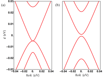
Finally, we discuss the in-plane spin–orbit interaction in Eq. (33). In our estimate for group IV-TMD–graphene bilayers this type of coupling is relatively weak, being of the same order of the in-plane spin–valley term ( 1 meV). However, it has interesting topological properties. As mentioned above, this SOC can induce a nontrivial topological insulating gap associated to a spin Chern number Sheng_06 . However, the robustness of the topological phase differs from that generated by the familiar intrinsic SOC in graphene KaneMele1 . When only -invariant SOCs are present, that is and , the quantum spin Hall gap closes if KaneMele1 , destroying the topological phase; see Fig. 5 (a). On the other hand, if the topological phase is a consequence of , the gap remains finite for any value of and as long as . A typical band structure is shown in Fig. 5(b), where the topological gap is finite even for large Bychkov-Rashba coupling. is one of the main obstacles to the observation of quantum spin Hall effect in graphene because of its interplay with . Our analysis suggest that realistic hybrid graphene–TMD bilayers can host a novel type of quantum spin Hall insulator with fully in-plane helical edge states.
VI Conclusion
We studied theoretically proximity spin–orbital effects in graphene placed on low-symmetry substrates with broken orbital degeneracy. We derived a low-energy (long-wavelength) theory for an idealized monolayer substrate, which allowed us to demonstrate a simple mechanism to remove the rotational invariance of electronic states in proximity-coupled graphene, i.e., their hybridization to crystal-field split states. The low symmetry environment was shown to render spin–orbit interactions of -electrons highly anisotropic. The most distinctive signature of the crystal field effect is the appearance of in-plane Zeeman ’spin–valley’ interaction and anisotropic intrinsic-type spin-orbit coupling , which can drive a transition to a quantum spin Hall insulating phase displaying in-plane helical edge states. As a possible candidate to observe the predicted effects, we suggested group IV TMD monolayers, where transition metal atoms have an octahedral distortion and contain the necessary ingredients to induce anisotropic in-plane SOCs on graphene.
Acknowledgments
T. G. R. acknowledges the support from the Newton Fund and the Royal Society (U.K.) through the Newton Advanced Fellowship scheme (ref. NA150043), T. P. C. and T. G. R. thank the Brazilian Agency CNPq for financial support. A.F. gratefully acknowledges the support from the Royal Society (U.K.) through a Royal Society University Research Fellowship.
Appendix
VI.1 Hopping parameters and -states.
The explicit expressions for the hopping parameters in Eq. (11) for the hollow-position case are
| (40) | |||
| (41) | |||
| (42) | |||
| (43) | |||
| (44) |
with constants , and given in Sec. III. -states of Eq. (11) can be written in terms of hexagonal states
| (45) |
with well-defined angular momentum and are described in reference Pachoud2014 . Using Eqs. (40-44), we have
| (46) | |||
| (47) | |||
| (48) | |||
| (49) | |||
| (50) |
We now move gears to the top-position case. Due to conservation of angular momentum, and are non-zero only for , , and . The explicit expressions of are
| (51) | |||
| (52) | |||
| (53) | |||
| (54) | |||
| (55) |
The explicit expressions of are
| (56) | |||
| (57) | |||
| (58) | |||
| (59) | |||
| (60) |
The constants of Eqs (51-55) are , , and , and by exchanging , for constants in (56-60).
-states of Eq (26) can be write in terms of triangular states Pachoud2014 ,
| (61) | |||
| (62) |
Here, are given by , , and . States (61) and (62), similarly to states (45), have well defined angular momentum and satisfy , and . In other words, graphene does not support triangular states with Pachoud2014 . Finally, we find
| (63) | |||
| (64) | |||
| (65) | |||
| (66) | |||
| (67) |
and,
| (68) | |||
| (69) | |||
| (70) | |||
| (71) | |||
| (72) |
References
- (1) P. Fazekas, Lecture Notes on Electron Correlation and Magnetism (World Scientific, Singapore, 1999).
- (2) E. Dagotto, Rev. Mod. Phys. 66, 763 (1994).
- (3) F. C. Zhang and T. M. Rice, Phys. Rev. B 37, 3759 (R) (1988).
- (4) R. Sachidanandam, T. Yildirim, A. B. Harris, A. Aharony, and O. Entin-Wohlman, Phys. Rev. B 56, 260 (1997).
- (5) P. Sati, et al., Phys. Rev. Lett. 96, 017203 (2006).
- (6) S. Ishihara, J. Inoue, and S. Maekawa, Phys. Rev. B 55, 8280 (1997).
- (7) M. B. Salamon and M. Jaime, Rev. Mod. Phys. 73, 583 (2001).
- (8) H. Jahn, and E. Teller, Phys. Rev. 49,874 (1936).
- (9) M. Ishizuka, I. Yamada, K. Amaya, and S. Endo, J. Phys. Soc. Japan 65, 1927 (1996).
- (10) G A Gehring and K A Gehring, Rep. Prog. Phys. 38, 1 (1975).
- (11) A. B. Cahaya, A. O. Leon, and G. E. W. Bauer, Phys. Rev. B 96, 144434 (2017).
- (12) D. Santos-Cottin, et al. Nature Communications 7, 11258 (2016).
- (13) C.-L. Song, et al., Appl. Phys. Lett. 97, 143118 (2010).
- (14) P. Lee, et al., ACS Nano 9, 10861 (2015).
- (15) S. Rajput, Y.-Y. Li, M. Weinert, and L. Li, ACS Nano, 10 8450 (2016).
- (16) D. Xiao, G.-B.Liu, W. Feng, X. Xu, and W. Yao. Phys. Rev. Lett. 108, 196802 (2012).
- (17) Q.H. Wang, et al. Nat. Nanotech. 7, 699 (2012).
- (18) K.F. Mak and J. Shan. Nat. Photon. 10, 216 (2016).
- (19) R. A. Muniz and J. E. Sipe, Phys. Rev. B 91, 085404 (2015).
- (20) M. Gmitra and J. Fabian, Phys. Rev. B 92, 155403 (2015).
- (21) A. Avsar, et al., ACS Nano 11, 11678 (2017).
- (22) Y. K. Luo, et al. Nano Lett. 17, 3877 (2017)
- (23) A. Avsar, et al., Nat. Commun. 5, 4875 (2014).
- (24) Z. Wang, D.-K. Ki, H. Chen, H. Berger, A. H. MacDonald, and A. F. Morpurgo, Nat. Commun. 6, 8339 (2015).
- (25) Z. Wang, D.-K. Ki, J. Y. Khoo, D. Mauro, H. Berger, L. S. Levitov, and A. F. Morpurgo, Phys. Rev. X 6, 041020 (2016).
- (26) S. Zihlmann, et al., Phys. Rev. B 97, 075434 (2018).
- (27) A. W. Cummings, J. H. Garcia, J. Fabian, and S. Roche, Phys. Rev. Lett. 119, 206601 (2017).
- (28) T. S. Ghiasi, J. Ingla-Aynes, A. Kaverzin, and B. J. van Wees, Nano Lett. 17, 7528 (2017).
- (29) L. A. Benitez, et al., Nature Physics 14, 303 (2018).
- (30) S. Omar and B. J. van Wees, Phys. Rev. B 97, 045414 (2018).
- (31) M. Milletari, M. Offidani, A. Ferreira, R. Raimondi, Phys. Rev. Lett. 119, 246801 (2017).
- (32) M. Offidani, M. Milletari, R. Raimondi, A. Ferreira, Phys. Rev. Lett. 119, 196801 (2017).
- (33) C. L. Kane and E. J. Mele, Phys. Rev. Lett. 95, 226801 (2005).
- (34) A. Pachoud, A. Ferreira, B. Ozyilmaz, and A. H. Castro Neto, Phys. Rev. B 90, 035444 (2014).
- (35) D. Kochan, S. Irmer, and J. Fabian. Phys. Rev. B 95, 165415 (2017).
- (36) E.L. Rashba, Phys. Rev. B 79, 161409(R) (2009).
- (37) M. Gmitra, D. Kochan, P. Hogl, and J. Fabian, Phys. Rev. B 93, 155104 (2016).
- (38) B. Hunt. et al. Science 340, 1427–1430 (2013).
- (39) J. Jung, A. M. DaSilva, A.H. MacDonald, and S. Adam. Nat. Comm. 6, 6308 (2015).
- (40) F. Calleja, et al., Nature Phys. 11, 43 (2015).
- (41) V. T. Phong, N. R. Walet, and F. Guinea, 2D Materials 5, 014004 (2017).
- (42) J. C. Slater and G. F. Koster, Phys. Rev. 94, 1498 (1954).
- (43) W. A. Harrison, Elementary Electronic Structure (World Scientific, Singapore, 2004).
- (44) G. Giovannetti, P. A. Khomyakov, G. Brocks, P. J. Kelly and J. van der Brink. Phys. Rev. B 76, 073103 (2007).
- (45) The relative strength of the proximity interactions at low energy is determined by the details of the hybridization between electronic states defined near the Dirac points (), which is independent of the electronic dispersion away from those points.
- (46) For convenience, the energy levels are defined with respect to the on-site energy of carbon atoms.
- (47) F. J. dos Santos, et al., arXiv:1712.07827 (2017).
- (48) A. H. Castro Neto, F. Guinea, N. M. R. Peres, K. S. Novoselov, and A. K. Geim, Rev. Mod. Phys. 81, 109 (2009).
- (49) E. Cappelluti, R. Roldan, J. A. Silva-Guillen, P. Ordejon, and F. Guinea, Phys. Rev. B 88, 075409 (2013).
- (50) J. A. Silva-Guillen, P. San-Jose, and R. Roldan, Applied Sciences 6, 284 (2016).
- (51) C. Gong, H. Zhang, W. Wang, L. Colombo, R. M. Wallace, and K. Cho, App. Phys. Lett 103,053513 (2013).
- (52) Y. J. Zhang, M. Yoshida, R. Suzuki, and Y. Iwasa, 2D Materials 2, 044004 (2015).
- (53) Y. Li, J. Kang, and J. Li, RSC Adv. 4, 7396 (2014).
- (54) H. Jiang, J. Chem. Phys., 134, 204705 (2011).
- (55) A. Kumar, H. He, R. Pandey, P. K. Ahluwalia, and K. Tankeshwar, Phys. Chem. Chem. Phys. 17, 19215 (2015).
- (56) X. Qian, J. Liu, L. Fu, and J. Li, Science 346, 1344 (2014).
- (57) S. Wu, et al., Science 359, 76 (2018).
- (58) H.-Y. Yang, C. Huang, H. Ochoa, and M. A. Cazalilla Phys. Rev. B 93, 085418 (2016).
- (59) D. H. Le, C. Colinet, and A. Pasturel, Physica B 168, 285 (1991).
- (60) D. N. Sheng, Z. Y. Weng, L. Sheng, and F. D. M. Haldane. Phys. Rev. Lett. 97, 036808 (2006).