Signature of Fermi arc surface states in Andreev reflection at the WTe2 Weyl semimetal surface.
Abstract
We experimentally investigate charge transport through the interface between a niobium superconductor and a three-dimensional WTe2 Weyl semimetal. In addition to classical Andreev reflection, we observe sharp non-periodic subgap resistance resonances. From an analysis of their positions, magnetic field and temperature dependencies, we can interpret them as an analog of Tomasch oscillations for transport along the topological surface state across the region of proximity-induced superconductivity at the Nb-WTe2 interface. Observation of distinct geometrical resonances implies a specific transmission direction for carriers, which is a hallmark of the Fermi arc surface states.
pacs:
73.40.Qv 71.30.+hI Introduction
Recent interest to Weyl semimetals is mostly connected with topological surface properties armitage . Weyl semimetals are conductors which, like other topological materials hasan ; zhang ; das ; chiu , are characterized by topologically protected conducting surface states. The concept of Weyl semimetals has been extended to type II materials armitage , like MoTe2 and WTe2, where constant energy surfaces are open electron and hole pockets with a Weyl point at their touching. Weyl points are topologically protected and their projections on the surface Brillouin zone are connected by Fermi arc surface states. For these materials, surface states were demonstrated in several experiments wang ; wu , although their topological nature is stil debatable bruno ; li . In contrast to three-dimensional topological insulators hasan described by invariant, Weyl surface states inherit the chiral property of the Chern insulator edge states armitage .
Topological materials exhibit non-trivial physics in proximity with a superconductor SNS1 ; SNS2 ; kundu . For a single normal-superconductor (NS) contact, Andreev reflection andreev allows low-energy electron transport from normal metal to superconductor by creating a Cooper pair, so a hole is reflected back to the normal side of the junction tinkham . The process can be more complicated heslinga if Andreev transport goes through an intermediate conductive region, e.g., the topological surface state at the NS interface klapwijk17 ; nbsemi ; ingasb . Also, geometrical resonances are predicted adroguer ; melnikov within the topological surface state in proximity with a superconductor, analogous to classical Tomasch tomasch1 ; tomasch2 ; tomasch_exp1 ; tomasch_exp2 effect.
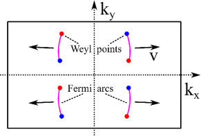
allows only internodal transport at the junction of the Weyl semimetal with a superconductor
Here, we experimentally investigate charge transport through the interface between a niobium superconductor and a three-dimensional WTe2 Weyl semimetal. In addition to classical Andreev reflection, we observe sharp non-periodic subgap resistance resonances. From an analysis of their positions, magnetic field and temperature dependencies, we can interpret them as an analog of Tomasch oscillations for transport along the topological surface state across the region of proximity-induced superconductivity at the Nb-WTe2 interface. Observation of distinct geometrical resonances implies a specific transmission direction for carriers, which is a hallmark of the Fermi arc surface states.
II Samples and technique
WTe2 compound was synthesized from elements by reaction of metal with tellurium vapor in the sealed silica ampule. The WTe2 crystals were grown by the two-stage iodine transport growth1 , that previously was successfully applied growth1 ; growth2 for growth of other metal chalcogenides like NbS2 and CrNb3S6. The WTe2 composition is verified by energy-dispersive X-ray spectroscopy. The X-ray diffraction (Oxford diffraction Gemini-A, MoK) confirms orthorhombic single crystal WTe2 with lattice parameters Å, Å, and Å.
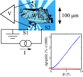
A sample sketch is presented in Fig. 1. We use dc magnetron sputtering to deposit a 70 nm thick niobium film on the insulating SiO2 substrate. Superconducting leads are formed by lift-off technique. A WTe2 single crystal ( dimensions) is weakly pressed to the niobium leads pattern, so the planar Nb-WTe2 junctions (with area) are formed at the bottom surface of the WTe2 crystal.
We study electron transport across a single Nb-WTe2 junction in a standard three-point technique, see Fig. 1 (c): the studied contact is grounded and two other contacts are used for applying current (below 100 A) and measuring WTe2 potential. To obtain characteristics, the dc current is additionally modulated by a low ac (0.5 A, 1.2 kHz) component. We measure both, dc () and ac () components of the WTe2 potential by using a dc voltmeter and a lock-in, respectively. We check, that the lock-in signal is independent of the modulation frequency in the 500 – 2500 Hz range, which is defined by applied ac filters.
To extract features specific to WTe2 Weyl semimetal surface states, the measurements are performed in a dilution refrigerator covering 30 mK–1.2 K temperature range. We check by standard magnetoresistance measurements that our WTe2 samples demonstrate large, non-saturating positive magnetoresistance in normal magnetic field, which goes to zero in parallel one, see inset to Fig. 1, as it has been shown for WTe2 Weyl semimetal mazhar .
III Experimental results
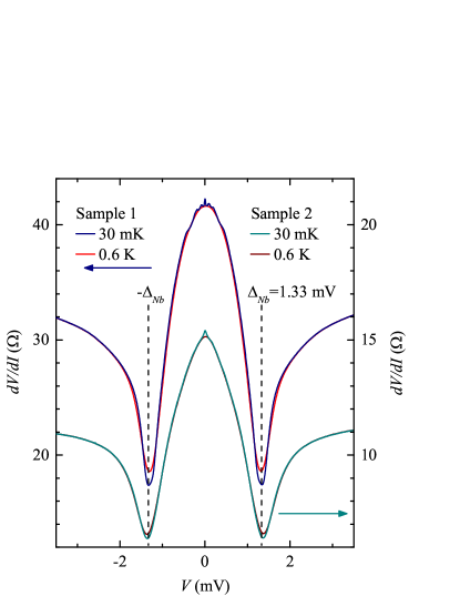
Examples of characteristics are shown in Fig. 2 for two different junctions with different . The obtained curves are verified to be independent of the mutual positions of the current/voltage, so they only reflect the transport parameters of the grounded Nb-WTe2 junction.
The main behavior is consistent with the standard one tinkham of a single Andreev junction: every curve demonstrates a clearly defined superconducting gap 1.33 mV (denoted by dashed lines), which is in a good correspondence with the expected K for niobium. The the subgap resistance is undoubtedly finite, which is only possible due to Andreev reflection. It exceeds the normal resistance value, so single-particle scattering is significant at the Nb-WTe2 interface tinkham . The interface scattering is expected, since the sputtered niobium is natively oxidized prior to placing a WTe2 single crystal onto the Nb leads pattern. A transmission of the interface can be estimated as for these junctions, which corresponds to the BTK barrier strength tinkham .
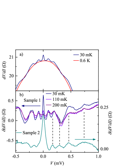
Specifics of the WTe2 Weyl semimetal appears as sharp subgap resistance resonances, see Figs. 2 and 3, which can not be expected tinkham for single Andreev NS contact. The resonances are suppressed completely above 0.6 K. Since the general behavior of curves is not sensitive to temperature much below K, see Fig. 2, the resonances can be analyzed in detail by subtracting the high-temperature (0.6 K) monotonous curve from the low-temperature (30 mK) one. The result () is shown in Fig. 3 (b) for the junctions from Fig. 2, the positions of the resonances are denoted by dashed lines. They are concentrated strictly within the superconducting gap and is a maximum at zero bias, the distance between the resonances is obviously increasing with bias in Fig. 3 (b). The number of visible resonances is different for different junctions. With increasing temperature, the amplitude of every resonance is diminishing, while its position is invariant, see Fig. 3 (b).
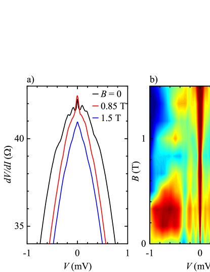
curves are shown in Fig. 4 (a) for different magnetic fields, oriented along a-axis of the crystal. In contrast to temperature suppression, the zero-bias peak survives above 0.85 T, while the resonances disappear completely. Moreover, curve still demonstrates non-trivial shape even for higher fields, with non-zero first derivative at zero bias, which also differs from temperature suppression. This evolution is shown in Fig. 4 (b) as colormap. The oscillations’ positions are constant up to their disappearance at 0.85 T, while superconductivity is completely suppressed around 4 T magnetic field in our samples.
IV Discussion
As a result, we observe pronounced subgap resonances for well-developer Andreev curves for a single Nb- SN junction. In general, resonance conditions require particle propagation between two different (SN or NN) interfaces.
For a thin crystal, it is naturally to think about vertical transport, normal to the Nb- interface. In this case, both Tomasch tomasch1 ; tomasch2 and MacMillan-Rowell mcmillan1 ; mcmillan2 geometrical resonances could be anticipated, which originates tomasch1 ; mcmillan1 ; mcmillan2 ; tomasch_exp1 ; tomasch_exp2 due to the space restriction in the S or N regions, respectively. However, these geometrical resonances should be observed at energies above the niobium superconducting gap, which contradicts to the experimental observations in Fig. 2. Also, MacMillan-Rowell oscillations mcmillan1 ; mcmillan2 ; osbite for bulk carriers in the WTe2 crystal are strictly periodic, which is is obviously not the case in Fig. 3.
Another possibility is multiple Andreev reflections tinkham (MAR), but the experimental curves are invariant to the choice of the potential contact. The resonance positions in Fig. 3 (b) does not correspond to the MAR sequence . Significant single-particle scattering at the Nb-WTe2 interface is inconsistent with MAR observation conditions for highly separated (more then 5 m) Nb contacts.
Thus, the observed resonances requires relation to surface states at the Nb- interface. WTe2 is regarded as type-II Weyl semimetal wang ; mazhar ; wang-miao hosting topological Fermi arcs states on (001) surfaces soluyanov , which was demonstrated in several experiments wu ; wang . In this case, an analog of Tomasch oscillations is allowed for transport along the topological surface state across the region of proximity-induced superconductivity near the niobium superconducting lead adroguer ; melnikov .
The resonances appear as Fabry-Perot-type transmission resonances for Bogoliubov quasiparticles in a long single NS junction, is a coherence length. They are situated adroguer ; melnikov at energies , where , is the Fermi velocity. According to this relation, the induced gap is reflected by the zero-bias structure heslinga ; klapwijk17 ; ingasb in Fig. 3. By fitting the resonance positions, we obtain meV, the effective junction dimension as m for (from ARPES databruno ).
This value is comparable with the dimensions of the planar Nb- junction (below m), taking in mind that placing on top of Nb does not guarantee good contact at all the surface. m is also about the mean free path along the a-axis in . It much exceeds the coherence length kulik-long ; dubos nm, which is obligatory to observe Tomasch oscillations for transport along the topological surface state adroguer ; melnikov .
The crucial point is that transmission resonances implies well-defined junction length . For the planar NS junction without axial symmetry, (nearly rectangular in our case), is different in different directions, which should smear the resonances for trivial surface states, e.g., originating from band bending near the WTe2 surface. On the other hand, Weyl surface states inherit the chiral property of the Chern insulator edge states armitage , where the preferable directions is defined by Fermi arcs on a particular crystal surface. In WTe2, the Weyl point are aligned along the -axis li of the crystal, forming preferable directions for surface carriers along the -axis, see Fig. 5. Thus, observation of sharp subgap resonances is specific for topological transport within the Fermi arc surface states at the Nb- interface. Since the resonances are defined by the interference effects, they are obviously suppressed in magnetic field above 0.85 T see Fig. 4. However, the curve evolution in higher fields is unusual for Andreev reflection and requires further investigations.
V Conclusion
As a conclusion, we experimentally investigate charge transport through the interface between a niobium superconductor and a three-dimensional WTe2 Weyl semimetal. In addition to classical Andreev reflection, we observe sharp non-periodic subgap resistance resonances. From an analysis of their positions, magnetic field and temperature dependencies, we can interpret them as an analog of Tomasch oscillations for transport along the topological surface state across the region of proximity-induced superconductivity at the Nb-WTe2 interface. Observation of distinct geometrical resonances implies a specific transmission direction for carriers, which is a hallmark of the Fermi arc surface states.
Acknowledgements.
We wish to thank V.T. Dolgopolov, V.A. Volkov, I. Gornyi, and A.S. Melnikov for fruitful discussions, and S.S Khasanov for X-ray sample characterization. We gratefully acknowledge financial support by the RFBR (projects 16-02-00405 and 18-02-00368) and RAS.References
- (1) As a recent review see N. P. Armitage, E. J. Mele, and Ashvin Vishwanath, Reviews of Modern Physics (2017), arxiv:1705.01111
- (2) M. Z. Hasan and C. L. Kane, Rev. Mod. Phys. 82, 3045 (2010).
- (3) X.-L. Qi and S.-C. Zhang, Rev. Mod. Phys. 83, 1057 (2011).
- (4) A. Bansil, H. Lin, and T. Das, Rev. Mod. Phys. 88, 021004 (2016).
- (5) C.-K. Chiu, J. C. Teo, A. P. Schnyder, and S. Ryu, Rev. Mod. Phys. 88, 035005 (2016).
- (6) Deng K., Wan G., Deng P., Zhang K., Ding S., Wang E., Yan M., Huang H., Zhang H., Xu Z., Denlinger J., Fedorov A., Yang H., Duan W., Yao H., Wu Y., Fan S., Zhang H., Chen X., Zhou S., Nat. Phys. 12, 1105–1110 (2016).
- (7) Ch. Wang, Y. Zhang, J. Huang, S. Nie, G. Liu, A. Liang, Yu. Zhang, B. Shen, J. Liu, C. Hu, Y. Ding, D. Liu, Y. Hu, S. He, L. Zhao, L. Yu, J. Hu, J. Wei, Z. Mao, Y. Shi, X. Jia, F. Zhang, S. Zhang, F. Yang, Z. Wang, Q. Peng, H. Weng, X. Dai, Z. Fang, Z. Xu, C. Chen, and X.J. Zhou, Phys. Rev. B 94, 241119(R) (2016).
- (8) Y. Wu, D. Mou, N.H. Jo, K. Sun, L. Huang, S.L. Bud’ko, P.C. Canfield, A. Kaminski, Phys. Rev. B 94, 121113(R) (2016).
- (9) F.Y. Bruno, A. Tamai Q.S. Wu, I. Cucchi, C. Barreteau, A. de la Torre, S. McKeown Walker, S. Riccò, Z. Wang, T.K. Kim, M. Hoesch, M. Shi, N.C. Plumb, E. Giannini, A.A. Soluyanov, and F. Baumberger, Phys. Rev. B 94, 121112(R) (2016).
- (10) P. Li, Y. Wen, X. He, Q. Zhang, C. Xia, Z. Yu, S. Yang, Z. Zhu, H. Alshareef, X. Zhang, Nature Com. 8, 2150 (2017).
- (11) Sean Hart, Hechen Ren, Timo Wagner, Philipp Leubner, Mathias Mühlbauer, Christoph Brüne, Hartmut Buhmann, Laurens W. Molenkamp & Amir Yacoby, Nature Physics 10, 638–643 (2014), doi:10.1038/nphys3036
- (12) Vlad S. Pribiag, Arjan J. A. Beukman, Fanming Qu, Maja C. Cassidy, Christophe Charpentier, Werner Wegscheider & Leo P. Kouwenhoven, Nature Nanotechnology 10, 593 (2015)
- (13) Udit Khanna, Dibya Kanti Mukherjee, Arijit Kundu, and Sumathi Rao Phys. Rev. B 93, 121409.
- (14) A. F. Andreev, Soviet Physics JETP 19, 1228 (1964).
- (15) M. Tinkham, Introduction to Superconductivity (2d ed., McGraw–Hill, New York, 1996).
- (16) D.R. Heslinga, S.E. Shafranjuk, H. van Kempen, and T.M. Klapwijk, Phys. Rev. B 49, 10484 (1994).
- (17) J. Wiedenmann, E. Liebhaber, J.s Kübert, E. Bocquillon, Ch. Ames, H. Buhmann, T.M. Klapwijk, L.W. Molenkamp, arXiv:1706.01638.
- (18) A. Kononov, S. V. Egorov, Z. D. Kvon, N. N. Mikhailov, S. A. Dvoretsky, and E. V. Deviatov, Phys. Rev. B 93, 041303(R) (2016)
- (19) A. Kononov, V.A. Kostarev, B.R. Semyagin, V.V. Preobrazhenskii, M.A. Putyato, E.A. Emelyanov, and E.V. Deviatov, Physical Review B 96, 245304 (2017). DOI: 10.1103/PhysRevB.96.245304
- (20) P. Adroguer, C. Grenier, D. Carpentier, J. Cayssol, P. Degiovanni, and E. Orignac, Phys. Rev. B 82, 081303(R), (2010).
- (21) N. B. Kopnin and A. S. Melnikov, Phys. Rev. B 84, 064524 (2011)
- (22) O.O. Shvetsov, V.A. Kostarev, A. Kononov, V.A. Golyashov, K.A. Kokh, O.E. Tereshchenko, and E.V. Deviatov, EPL 119, 57009 (2017), doi:10.1209/0295-5075/119/57009
- (23) W. J. Tomasch, Phys. Rev. Lett. 16, 16 (1966).
- (24) W. L. McMillan, P. W. Anderson, Phys. Rev. Lett. 16, 85 (1966).
- (25) O. Nesher, G. Koren, Phys. Rev. B 60, 9287 (1999).
- (26) C. Visani, Z. Sefrioui, J. Tornos, C. Leon, J. Briatico, M. Bibes, A. Barthélémy, J. Santamaría and Javier E. Villegas, Nature Physics, 8, 539 (2012), DOI: 10.1038/NPHYS2318
- (27) E. B. Borisenko, V. A. Berezin, N. N. Kolesnikov, V. K. Gartman, D. V. Matveev, O. F. Shakhlevich, Physics of the Solid State, 59, 1310, (2017).
- (28) A. Sidorov, A.E. Petrova, A.N. Pinyagin, N.N. Kolesnikov, S.S. Khasanov, S.M. Stishov, JETP, 122, 1047, (2016).
- (29) A. M. Toxen Phys. Rev. 123, 442 (1961).
- (30) J. M. Rowell, W. L. McMillan, Phys. Rev. Lett. 16, 453 (1966).
- (31) J. M. Rowell, Phys. Rev. Lett. 30, 167–170 (1973).
- (32) Mazhar N. Ali, Jun Xiong, Steven Flynn, Jing Tao, Quinn D. Gibson, Leslie M. Schoop, Tian Liang, Neel Haldolaarachchige, Max Hirschberger, N. P. Ong and R. J. Cava Nature 514, 205 (2014). doi:10.1038/nature13763
- (33) Wang, Y. et al., Nat. Commun. 7, 13142 (2016). doi: 10.1038/ncomms13142
- (34) A.A. Soluyanov, D. Gresch, Z. Wang, Q. Wu, M. Troyer, X. Dai, B.A. Bernevig, Nature 527, 495 (2015).
- (35) I. O. Kulik, Sov. Phys. JETP 30, 944 (1970).
- (36) P. Dubos, H. Courtois, B. Pannetier, F. K. Wilhelm, A. D. Zaikin, and G. Schön Phys. Rev. B 63, 064502 (2001)