Van der Waals spin valves
Abstract
We propose spin valves where a 2D non-magnetic conductor is intercalated between two ferromagnetic insulating layers. In this setup, the relative orientation of the magnetizations of the insulating layers can have a strong impact on the in-plane conductivity of the 2D conductor. We first show this for a graphene bilayer, described with a tight-binding model, placed between two ferromagnetic insulators. In the anti-parallel configuration, a band gap opens at the Dirac point, whereas in the parallel configuration, the graphene bilayer remains conducting. We then compute the electronic structure of graphene bilayer placed between two monolayers of the ferromagnetic insulator CrI3, using density functional theory. Consistent with the model, we find that a gap opens at the Dirac point only in the antiparallel configuration.
The controlled fabrication of layered structures combining ferromagnetic conductors and non magnetic materials, thin enough as to preserve spin polarization, made possible the discovery of fundamental spin dependent transport phenomena, such as Giant Magnetoresistance Baibich et al. (1988); Binasch et al. (1989) and tunnel Magnetoresistance Julliere (1975); Moodera et al. (1995). These developments led to the concept of spin valve, a structure whose conductivity is modulated by the relative orientation of two ferromagnetic electrodes Dieny et al. (1991) and, altogether, set the foundations of spintronics.
The study of the so called Van der Waals heterostructures Geim and Grigorieva (2013); Novoselov et al. (2016), metamaterials obtained by vertical stacking of 2D crystals, is a very fertile area of research. Using relatively simple fabrication methods, they allow the study of structures with tailored electronic properties that combine a variety of 2D materials, including insulators (h-BN), semiconductors (MoS2), conductors (graphene) and superconductors (NbSe2). The recent discovery of 2D crystals with magnetic order Wang et al. (2016); Lee et al. (2016); Gong et al. (2017); Huang et al. (2017) adds both ferromagnetic and antiferromagnetic insulators to this list. For instance, Van der Waals devices incorporating atomically thin layers of the ferromagnetic insulator CrI3, have being reportedKlein et al. (2018); Song et al. (2018); Wang et al. (2018); Jiang et al. (2018a); Huang et al. (2018); Jiang et al. (2018b). These findings pave the way to Van der Waals spintronics with new types of spin dependent transport phenomena.
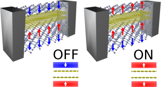
Here we propose a new class of spin valve that takes advantage of the spin proximity effect, i.e., the spin polarization of the surface electrons of a non-magnetic material adjacent to a ferromagnet. The proposed system, depicted in Figure 1, consists of a 2D conducting crystal sandwiched between two insulating ferromagnetic layers. If the magnetizations of the two proximity layers are anti-parallel (AF), the spin proximity effects have opposite sign at both sides of the 2D crystal. In contrast, for the parallel state (FM), the top and bottom proximity effects add up. As we show below, this difference has a strong influence in the in-plane conductance of the non-magnetic conductor, and in some instances leads to a conductor to insulator transition in the 2D crystal. This strong influence of spin proximity effect in a 2D crystals contrast with the case of 3D materials, for proximity effects are constrained to their surface.
Our proposal is different from lateral graphene spin valves Tombros et al. (2007); Han et al. (2014), where large areas of the graphene are not in contact with ferromagnetic electrodes, and is also different from spin-filter tunnel junctions, where the magnetic insulators act as barrier materials for vertical transport Miao et al. (2009); Klein et al. (2018); Song et al. (2018); Wang et al. (2018). The proposed spin valve resembles the early current in plane structures where giant magnetoresistance was discovered Baibich et al. (1988); Binasch et al. (1989), with the obvious difference that the magnetic layers are insulating in the Van der Waals spin valves.
We first illustrate the concept of Van der Waals (VdW) spin valves considering the case when the central conductor is a graphene bilayer. We use the standard tight-binding model for the graphene bilayerGuinea et al. (2006). Spin proximity effect is consideredPhong et al. (2017) by including a spin dependent potential whose sign can be different in the top and bottom graphene layers. Previous density functional theory (DFT) calculations for monolayer graphene deposited on different ferromagnetic insulators, such as EuOYang et al. (2013); Hallal et al. (2017), EuS Hallal et al. (2017), YIG Hallal et al. (2017), justify this model. We assume that the magnetization of both top and bottom layers lie on the same axis. We also assume that the bottom magnetization does not change, resulting in fixed spin-dependent potential , where is the spin projection along the magnetization axis. The top layer spin dependent potential is given by , where describes the magnetization orientation of the top magnetic layer, relative to the bottom layer. Thus, describes the parallel (FM) orientation and the antiparallel (AF) case.
Represented in the basis , where and correspond to the two triangular sublattices, and the subindices 1 and 2 label the top and bottom layers, respectively, the Bloch Hamiltonian for spin states reads:
| (5) |
where and describe the intralayer and interlayer hopping matrix elements, respectively. The resulting spin resolved energy bands, in the neighbourhood of the Dirac point, are shown in fig. 2 for the two states of the spin valve, . For the FM alignment (), the graphene bilayer presents spin-split bands, and remains in a conducting state,i.e., with a finite density of states at the Fermi energy. In contrast, for the AF case (), a band-gap opens up at the Dirac point. Thus, depending on the relative alignment of the top and bottom insulating ferromagnets, the graphene bilayer spin valve can be either a conductor, for the FM alignment, or a gapped system with depleted conductance, when the Fermi energy is set at the Dirac point. Within this model, both the band-gap in the AF alignment and the spin splitting in the FM alignment are given by .
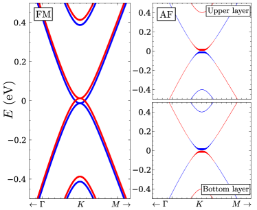
We now address the origin of the gap opening in graphene bilayer AF alignment of the VdW spin valve. For each spin channel, the Hamiltonian (5) in the AF alignment is identical to the model of graphene bilayer with an off-plane electric field, that is known to open up a gap in the band structure Ohta et al. (2006); McCann (2006). Interestingly, in the spin-valve, the sign of the effective electric field is opposite for opposite spins, . The spin projection of the AF bands over top and bottom layers, shown in Fig. 2, clearly shows the presence of a spin dipoleFernández-Rossier (2008): for a given spin, there is a charge imbalance driven by the exchange with the magnetic layers, that is compensated exactly by the opposite spin.
In a graphene bilayer, the gap opened by an electric field is known to have a valley dependent Chern number , where labels the valleys Martin et al. (2008); San-Jose et al. (2009). In the case of the spin valve in the AF state, this leads to Chern numbers that are both spin and valley dependent:
| (6) |
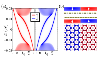
Eq. (6) permits to anticipate Martin et al. (2008); San-Jose et al. (2009) the emergence of spin-locked chiral one dimensional in gap states in domain walls separating two antiferromagnetic domains with opposite magnetizations (see Fig 3). In order to verify this, we compute the momentum resolved density of states of a domain wall along the zigzag direction as ilustrated in fig. 3. The domain wall is assumed to be abrupt, preserving spin collinearity. The calculation is done for a system with translational invariance along the wall direction, and embedded between two semi-infinite gapped graphene bilayer planes, using a Green function technique Lado et al. (2015). Both domains are insulating, but at each valley the Chern number is opposite for a given spin direction. Thus, a domain wall along the zigzag direction, that preserves the valley, features two chiral 1D in-gap states per valley and per spin (see fig. 3). It is interesting to note that, for a given valley, the states are spin chiral and therefore back-scattering requires either spin-mixing, or inter-valley scattering. A non collinear domain wall might result in spin mixing.
We now consider a possible physical realization of the Van der Waals spin valve, based on a graphene bilayer, that is feasible within the experimental state of the art. For that matter, we choose CrI3 monolayers as the insulating ferromagnet. It was recently shown that CrI3 monolayers remain ferromagnetic up to 45K Huang et al. (2017). In addition CrI3 preserves its magnetic properties even when deposited on graphite Huang et al. (2017) or encapsulated between graphite electrodes Klein et al. (2018); Song et al. (2018); Wang et al. (2018). Moreover, the spin proximity effect between CrI3 and two dimensional WSe2 has been demonstrated experimentally Zhong et al. (2017).
The DFT calculations were performed using Quantum ESPRESSO Giannozzi et al. (2009) with PBE exchange-correlation potential Perdew et al. (1996) and PAW pseudopotentials Blöchl (1994); Kucukbenli et al. (2014) and including van der Waals interactions within the semiempirical method of Grimme (DFT-D2) Grimme (2006). Spin orbit interactions, known to be important to determine the magnetic anisotropy of CrI3 Lado and Fernández-Rossier (2017), are not included in the calculation, as they are not expected to induce qualitative change in the spin proximity effect discussed here.
We now discuss our results both for monolayer CrI3 /monolayer graphene as well as graphene bilayer in between two monolayers of CrI3. The former permits to rationalize the results of the bilayer. For the bilayer, we use a unit cell with 4 layers, CrI3/graphene bilayer/CrI3, and two different geometries: 1) a free standing multilayer and 2) a superlattice with periodic boundary conditions along the off-plane direction. In the case of the superlattice with periodic boundary conditions, we considered the lattice parameter of graphene for the plane and varied the lattice parameter in order to optimize the interlayer distance by minimizing the total energy. For the free standing multilayer, we used a lattice parameter along that ensures the absence of interaction between the replicas of the system. In all cases the unit cell contains a 33 supercell with 18 carbon atoms per graphene layer, 2 chromium and 6 iodine atoms per CrI3 layer. Thus, for the sandwiched graphene bilayer, the unit cell has a total of 52 atoms. The calculations show that the spin of Cr atoms is , that are hosted by the bands.
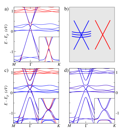
We first discuss the results for the monolayer graphene on top of CrI3, shown in (3)(a). Our results are in line with previous DFT calculations for this system Zhang et al. (2017). With the exception of some anti-crossings, the energy bands are an overlay of those of the decoupled monolayers, as expected in a Van der Waals structure. Occupied bands, way below the Fermi energy , are made of iodine states and the spin majority states of Cr. Empty bands, high above , are made of spin minority states of Cr. In the 2 eV window around the Fermi energy, the bands are those of the graphene Dirac cones and the spin majority states. These four bands (coming from 2 Cr atoms in the unit cell) are narrow, lie almost completely above the Fermi energy, and hybdridize with the graphene Dirac cones in the majority spin channel close to the Dirac point. In contrast, the minority spin Dirac cone remains intact (see cartoon in (4)(b). Therefore, for one spin channel the Dirac electrons barely notice the presence of the CrI3, for the other spin channel, there is a strong hybdrization with a narrow band.
The bands structure of the CrI3/graphene bilayer/CrI3 are shown in figure (3), both for the FM (left) and AF (right) configurations. Both of them show the graphene bilayer bands and the bands. For the FM case, the shape of the graphene bilayer bands is preserved in one spin channel (the minority spin), but a strong hybridization opens up a gap in the majority spin channel, slightly above the Fermi energy, which lies below the Dirac point. For the AF configuration, both spin channels of the graphene bilayer become hybdridized with the narrow bands of CrI3. So, from that point of view alone, we expect that the in-plane conductance is much larger in the FM alignment than the AF one.
We now turn our attention to the states around the Dirac energy, where the conduction and valence parabolic bands of freestanding graphene bilayer meet. For the AF configuration, a band-gap splits the electron and hole parabolic of graphene bilayer (see inset of Fig. (4d)), with a gap of 7 . For the FM configuration, there is a spin splitting of the bands near the Dirac point, whose magnitude is, interestingly, the same, than the AF gap. So, in that regard, the DFT results for the bilayer graphene placed between two CrI3 layers are in line with the toy model. However, there is electron transfer from graphene to CrI3, so that the Fermi energy does not lie at the Dirac point. It must be noticed that, even if there is charge transfer, we expect a very small in-plane conductance in the CrI3, on account of the very small dispersion of the occupied states.
Thus, our DFT calculations strongly suggest that a graphene bilayer encapsulated between two layers of CrI3 will present a strong spin-valve effect, with the FM alignment having a larger in-plane conductance, on account of the fact that bands in one spin-channel are decoupled from the non-dispersive CrI3 bands, in contrast with the AF, where both spin channels are hybdridized. Interestingly, the same mechanism should also apply for the graphene monolayer. In addition, for the graphene bilayer, application of a gate voltage could set the Fermi energy at the Dirac point, resulting in a conductor to insulator transition driven by the alignment of the magnetizations.
The control of the relative orientation of the magnetization of the layers could be done by application of a magnetic field, provided that two conditions are met. First, the interlayer coupling should be smaller than the Zeeman coupling. Interlayer coupling of CrI3 bilayers, without graphene in the middle, meets this demand. The presence of the graphene bilayer should significantly reduce the interlayer coupling. Accordingly, our DFT calculations yield eV per unit cell. Second, the switching field of top and bottom layers should be different. A very natural way to achieve that is to pin the magnetization of the bottom layer. This could be done, for instance, using a bilayer of CrI3 for which antiferromagnetic interlayer coupling has been reported Huang et al. (2017); Klein et al. (2018); Jiang et al. (2018a); Huang et al. (2018); Jiang et al. (2018b)
The concept of Van der Waals spin valve goes beyond the case of the graphene bilayer. For instance, the tunable spin proximity effect can drive a metal insulator transition in a graphene monolayer in the Quantum Hall regime. At half filling, high quality graphene quantum Hall bars are often insulating. Application of a strong in-plane magnetic field can induce a Quantum Hall ferromagnet that has a finite edge conductance Young et al. (2014); Lado et al. (2015). In a spin valve, such transition could be promoted by spin proximity effect, rather than Zeeman interaction. Another possibility are Van der Waals spin valves with a superconducting middle layer, such as NbSe2. In the FM state, spin proximity effect can kill superconductivity, that would only survive in the AF state. Such a transition has been observed in superconducting thin films sandwiched between bulk ferromagnetic insulators Li et al. (2013). The concept of Van der Waals spin valve can be extended to the control of optical properties. For instance, spin proximity might control whether dark or bright excitons of the middle layer are the ground state of the 2D semiconductor.
In conclusion, we have proposed a new type of spin valve where a non-magnetic 2D crystal is sandwiched between two ferromagnetic insulators and its in-plane conductance is controlled by spin proximity effect. We hope that our work will motivate the experimental exploration of Van der Waals current in plane spin valves, including the of other materials in the non-magnetic layers, such as superconductors, as well as other magnetic layers, such as bulk ferrromagnets, for which the spin valve effect proposed here should also work.
We acknowledge J. L. Lado for fruitful discussions and technical assistance in the calculations. We acknowledge financial support from FEDER project NORTE-01-0145-FEDER-000019, the Marie Curie Nano TRAIN for Growth Cofund program at INL and FCT for the P2020-PTDC/FIS-NAN/3668/2014 project. We acknowledge Efrén Navarro-Morata for fruitful discussions.
References
- Baibich et al. (1988) M. N. Baibich, J. M. Broto, A. Fert, F. N. Van Dau, F. Petroff, P. Etienne, G. Creuzet, A. Friederich, and J. Chazelas, Physical Review Letters 61, 2472 (1988).
- Binasch et al. (1989) G. Binasch, P. Grünberg, F. Saurenbach, and W. Zinn, Physical Review B 39, 4828 (1989).
- Julliere (1975) M. Julliere, Physics Letters A 54, 225 (1975).
- Moodera et al. (1995) J. S. Moodera, L. R. Kinder, T. M. Wong, and R. Meservey, Physical Review Letters 74, 3273 (1995).
- Dieny et al. (1991) B. Dieny, V. S. Speriosu, S. Metin, S. S. Parkin, B. A. Gurney, P. Baumgart, and D. R. Wilhoit, Journal of Applied Physics 69, 4774 (1991).
- Geim and Grigorieva (2013) A. K. Geim and I. V. Grigorieva, Nature 499, 419 (2013).
- Novoselov et al. (2016) K. Novoselov, A. Mishchenko, A. Carvalho, and A. C. Neto, Science 353, aac9439 (2016).
- Wang et al. (2016) X. Wang, K. Du, Y. Y. F. Liu, P. Hu, J. Zhang, Q. Zhang, M. H. S. Owen, X. Lu, C. K. Gan, P. Sengupta, et al., 2D Materials 3, 031009 (2016).
- Lee et al. (2016) J.-U. Lee, S. Lee, J. H. Ryoo, S. Kang, T. Y. Kim, P. Kim, C.-H. Park, J.-G. Park, and H. Cheong, Nano Letters 16, 7433 (2016).
- Gong et al. (2017) C. Gong, L. Li, Z. Li, H. Ji, A. Stern, Y. Xia, T. Cao, W. Bao, C. Wang, Y. Wang, et al., Nature 546, 265 (2017), ISSN 0028-0836.
- Huang et al. (2017) B. Huang, G. Clark, E. Navarro-Moratalla, D. R. Klein, R. Cheng, K. L. Seyler, D. Zhong, E. Schmidgall, M. A. McGuire, D. H. Cobden, et al., Nature 546, 270 (2017).
- Klein et al. (2018) D. R. Klein, D. MacNeill, J. L. Lado, D. Soriano, E. Navarro-Moratalla, K. Watanabe, T. Taniguchi, S. Manni, P. Canfield, J. Fernández-Rossier, et al., arXiv preprint arXiv:1801.10075 (2018).
- Song et al. (2018) T. Song, X. Cai, M. W.-Y. Tu, X. Zhang, B. Huang, N. P. Wilson, K. L. Seyler, L. Zhu, T. Taniguchi, K. Watanabe, et al., arXiv preprint arXiv:1801.08679 (2018).
- Wang et al. (2018) Z. Wang, I. Gutiérrez-Lezama, N. Ubrig, M. Kroner, T. Taniguchi, K. Watanabe, A. Imamoğlu, E. Giannini, and A. F. Morpurgo, arXiv preprint arXiv:1801.08188 (2018).
- Jiang et al. (2018a) S. Jiang, J. Shan, and K. F. Mak, Nature materials (2018a).
- Huang et al. (2018) B. Huang, G. Clark, D. R. Klein, D. MacNeill, E. Navarro-Moratalla, K. L. Seyler, N. Wilson, M. A. McGuire, D. H. Cobden, D. Xiao, et al., arXiv:1802.06979v2 [cond-mat.mes-hall] (2018).
- Jiang et al. (2018b) S. Jiang, L. Li, Z. Wang, K. F. Mak, and J. Shan, arXiv:1802.07355v1 (2018b).
- Tombros et al. (2007) N. Tombros, C. Jozsa, M. Popinciuc, H. T. Jonkman, and B. J. Van Wees, Nature 448, 571 (2007).
- Han et al. (2014) W. Han, R. K. Kawakami, M. Gmitra, and J. Fabian, Nature nanotechnology 9, 794 (2014).
- Miao et al. (2009) G.-X. Miao, M. Müller, and J. S. Moodera, Phys. Rev. Lett. 102, 076601 (2009).
- Guinea et al. (2006) F. Guinea, A. C. Neto, and N. Peres, Physical Review B 73, 245426 (2006).
- Phong et al. (2017) V. T. Phong, N. R. Walet, and F. Guinea, 2D Materials 5, 014004 (2017).
- Yang et al. (2013) H. Yang, A. Hallal, D. Terrade, X. Waintal, S. Roche, and M. Chshiev, Physical Review Letters 110, 046603 (2013).
- Hallal et al. (2017) A. Hallal, F. Ibrahim, H. Yang, S. Roche, and M. Chshiev, 2D Materials 4, 025074 (2017).
- Ohta et al. (2006) T. Ohta, A. Bostwick, T. Seyller, K. Horn, and E. Rotenberg, Science 313, 951 (2006).
- McCann (2006) E. McCann, Phys. Rev. B 74, 161403 (2006).
- Fernández-Rossier (2008) J. Fernández-Rossier, Physical Review B 77, 075430 (2008).
- Martin et al. (2008) I. Martin, Y. M. Blanter, and A. Morpurgo, Physical Review Letters 100, 036804 (2008).
- San-Jose et al. (2009) P. San-Jose, E. Prada, E. McCann, and H. Schomerus, Physical Review Letters 102, 247204 (2009).
- Lado et al. (2015) J. L. Lado, N. García-Martínez, and J. Fernández-Rossier, Synthetic Metals 210, 56 (2015).
- Zhong et al. (2017) D. Zhong, K. L. Seyler, X. Linpeng, R. Cheng, N. Sivadas, B. Huang, E. Schmidgall, T. Taniguchi, K. Watanabe, M. A. McGuire, et al., Science Advances 3, e1603113 (2017).
- Giannozzi et al. (2009) P. Giannozzi, S. Baroni, N. Bonini, M. Calandra, R. Car, C. Cavazzoni, D. Ceresoli, G. L. Chiarotti, M. Cococcioni, I. Dabo, et al., J. Phys.: Condens. Mat. 21, 395502 (2009).
- Perdew et al. (1996) J. P. Perdew, M. Ernzerhof, and K. Burke, J. Chem. Phys. 105, 9982 (1996).
- Blöchl (1994) P. E. Blöchl, Phys. Rev. B 50, 17953 (1994).
- Kucukbenli et al. (2014) E. Kucukbenli, M. Monni, B. Adetunji, X. Ge, G. Adebayo, N. Marzari, S. De Gironcoli, and A. D. Corso, arXiv preprint arXiv:1404.3015 (2014).
- Grimme (2006) S. Grimme, J. Comput. Chem. 27, 1787 (2006).
- Lado and Fernández-Rossier (2017) J. L. Lado and J. Fernández-Rossier, 2D Materials 4, 035002 (2017).
- Zhang et al. (2017) J. Zhang, B. Zhao, T. Zhou, Y. Xue, C. Ma, and Z. Yang, arXiv preprint arXiv:1710.06324 (2017).
- Young et al. (2014) A. Young, J. Sanchez-Yamagishi, B. Hunt, S. Choi, K. Watanabe, T. Taniguchi, R. Ashoori, and P. Jarillo-Herrero, Nature 505, 528 (2014).
- Li et al. (2013) B. Li, N. Roschewsky, B. A. Assaf, M. Eich, M. Epstein-Martin, D. Heiman, M. Münzenberg, and J. S. Moodera, Physical Review Letters 110, 097001 (2013).