In-situ tuning of individual position-controlled nanowire quantum dots via laser-induced intermixing
Abstract
We demonstrate an - technique to tune the emission energy of semiconductor quantum dots. The technique is based on laser-induced atomic intermixing applied to nanowire quantum dots grown using a site-selective process that allows for the deterministic tuning of individual emitters. A tuning range of up to 15 meV is obtained with a precision limited by the laser exposure time. A distinct saturation of the energy shift is observed, which suggests an intermixing mechanism relying on grown-in defects that are subsequently removed from the semiconductor material during annealing. The ability to tune different emitters into resonance with each other will be required for fabricating remote quantum dot-based sources of indistinguishable photons for secure quantum networks.
A prime motivator for the development of single photon sources is that of secure optical communications based on quantum key distribution (QKD). Implementations such as quantum repeater-basedLo and Chau (1999) entanglement distribution and measurement-device-independent QKDLo et al. (2012) require the generated photons to be indistinguishable one from the otherSantori et al. (2002) (i.e. perfect overlap of the photon wave-packets in all degrees of freedom: energy, time, space, polarization). Quantum dot-based sources are a promising candidate for implementation in QKD networks: they can be extremely efficient if incorporated within appropriate photonic environments i.e. cavitiesYoshie et al. (2001); Moreau et al. (2001), waveguidesG. et al. (2014), they have demonstrated high purity on-demand single photon emissionAharonovich et al. (2016) and sequentially emitted photons from the same dot can be highly indistinguishable when using resonant excitationLoredo et al. (2016); Wang et al. (2016).
For use in distributed QKD networks however, indistinguishable photons from separate quantum dots are required and this has proven challengingGold et al. (2014); Giesz et al. (2015); Thoma et al. (2017); Reindl et al. (2017) due to the variation in emission energy from dot to dot. Apart from selecting two quantum dots that happen to have the same emission energy, attempts have been made to dynamically tune two dots into resonance using controls such as applied strainFlagg et al. (2010) or electric-field Patel et al. (2010). An alternative to dynamic tuning is quantum dot intermixing which has been shown to be an effective method to tune emission energies over a wide spectral rangeHaysom et al. (2000, 2000); Dubowski et al. (2000); Girard et al. (2004); Dion et al. (2006, 2008, 2008). Intermixing is typically performed ex-situ by rapid thermal annealingGirard et al. (2004) but can also be done in-situ using a focused laserDubowski et al. (2000). - tuning with a focused laser has been demonstrated using quantum dot ensemblesRastelli et al. (2007).
In this study we investigate laser-induced intermixing processes in single InAsP/InP nanowire quantum dots. An InAsP/InP quantum dot is an inherently metastable system where if enough energy is provided, typically through heating, the As and P atoms will intermix through a diffusion process. This intermixing can be enhanced at lower temperatures by the presence of mobile crystal defects that are either already present (e.g. through judicious choice of crystal growth conditionsDion et al. (2006) or ion implantationDion et al. (2008)) or are thermally created. As these defects diffuse through the InAsP/InP quantum dot they cause an atomic mixing on the group V sites and hence a change in the emission energy of the dot. No change is observed on the group III sites since indium is the only group III atom present in these structures. This process is highly temperature dependent, with the creation of defects (typically at the semiconductor surface) requiring higher temperatures than the defect diffusion.
In addition to changes in emission energy, quantum dot intermixing can also affect material quality and lead to improved indistinguishability of the emitted photons. Defect states are known to trap carriers, leading to spectral fluctuations of the dot emission as the charge state fluctuates and reducing the indistinguishability of sequentially emitted photonsReimer et al. (2016). This is particularly relevant in InP-based nanowire devices, where growth temperatures required for vapor-liquid-solid (VLS) epitaxy are lower than in conventional growth, leading to a higher density of impurities and crystal defects (e.g. group V interstitialsDion et al. (2006)). Given that the low temperature intermixing process relies on the diffusion of grown-in defects and considering that these defects will eventually be annihilated or trapped at sinks such as exposed semiconductor surfaces, we expect that following the intermixing process we will be left with a material of improved crystal quality.
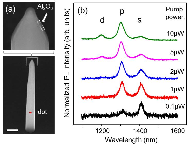
The InAsP/InP nanowire quantum dot devices used in this study were grown using a combined selective-area and VLS epitaxy approachDalacu et al. (2009, 2012) (see Methods). Importantly, the nanowires were grown using a position-controlled processDalacu et al. (2009) that ensures only a single nanowire within the intermixing laser spot, allowing for the tuning of individual quantum dots. To provide protection against surface decomposition during intermixing (see Supporting Information), the devices were coated with 40 nm of Al2O3 or SiO2, see Figure 1(a). Intermixing was carried out at a substrate temperatures of both 4 K and 300 K using a laser focused to a spot size of 2 m (see Methods). For the 300 K measurements, devices emitting at telecom wavelengthsHaffouz et al. were used. The confining potentials in these dots are sufficiently deep to allow observation of ground and excited state emission at room temperature. For the 4 K measurements, devices emitting around nm were used.
Room temperature, power-dependent photoluminescence (PL) spectra from a typical telecom quantum dot used in the room temperature intermixing experiments are shown in Figure 1(b). At low pump powers, the ground-state emission is observed at nm. With increasing pump power, the atomic-like level structure is clearly evidenced by the appearance of peaks at higher energy which correspond to recombination from excited levels (e.g. -shell and -shell).
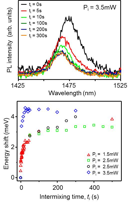
Ground-state emission wavelengths were determined from PL measurements at excitation powers , where nW is the power required to saturate the ground-state transition. Intermixing was achieved by exciting at powers for various times . The optical absorption of the pump laser in the nanowire resulted in a rapid heating to temperatures high enough to induce intermixingDion et al. (2006) (typically C). Figure 2(a) shows the 300 K PL from the ground state of a single nanowire dot as a function of for an intermixing laser power of mW using a 633 nm laser. In Figure 2(b), we show the dependence on intermixing time of the ground-state energy shift for four nanowire devices annealed at different powers. All devices show a blue-shift of the ground state energy of approximately 3 - 4 meV. The tuning behavior is non-linear, with the rate decreasing and the energy shift finally saturating with increasing intermixing time. The sample exposed to the highest optical power exhibits the highest initial tuning rate.
This behavior is typical of the intermixing process in InAsP/InP quantum dots with large numbers of grown-in P anti-site defectsDion et al. (2006, 2008, 2008). Upon annealing, P anti-site defects dissociate to form P interstitials and In vacancies. As mentioned above, the highly mobile P interstitials subsequently diffuse through the quantum dot where the atomic intermixing of the group V species changes the composition profile of the dot, blue-shifting the emission energy as the InAsP dot material becomes increasingly P rich. This group V intermixing process can be described within a Fickian diffusion modelDion et al. (2008), using a temperature dependent inter-diffusion length where is the inter-diffusion constant. If the source of defects enabling this diffusion process is never depleted then is constant with time and the dot will intermix until its composition is very close to InP. In the nanowire case however, we observe a distinct saturation of the energy shift with time, consistent with the depletion of inter-diffusion-promoting defects in the system. We note that the largest shift obtained, ( meV) covers a significant fraction of the standard deviation of the emission energies typically observed in the nanowire system, meVChen et al. (2016) allowing us to tune a large proportion of the nanowire dots to the same emission energy.
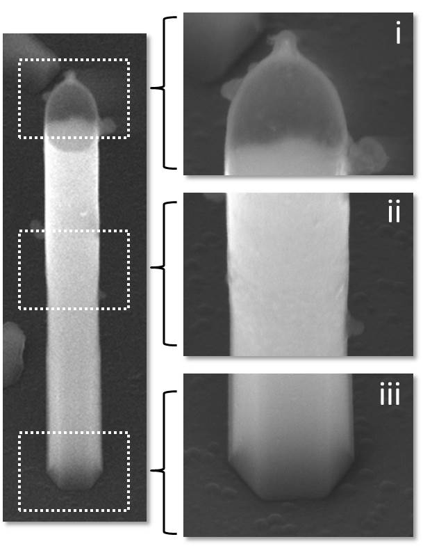
As well as an energy shift, the intermixing process in the nanowire devices also results in a large reduction in the PL intensity, clearly seen in Figure 2(a). The integrated intensities of the four samples in Figure 2(b) decrease by a factor of four after the first few seconds of intermixing. The decease in brightness can be understood by looking at the nanowire after annealing. A scanning electron microscopy (SEM) image of a nanowire that has been annealed is shown in Figure 3, where significant differences from the as-grown devices are observed. We identify three different regions on the nanowire: (i) the top, where the InP has melted and left behind an inflated Al2O3 shell complete with a Au catalyst nipple, (ii) the middle, where melted InP from above is trapped underneath the Al2O3 shell and (iii) the bottom, which is intact, complete with clearly observable crystallographic sidewall facets.
In Reference 23, the authors employed microdisk structures in which the pedestal limited the heat flow to the substrate. In such structures, the microdisk attains a uniform temperature which, for a given laser power, is determined by the thermal resistance of the pedestal. In the nanowire case, the temperature at a height above the substrate is expected to vary linearly according to (see Supporting Information):
| (1) |
where is the temperature of the substrate, is the nanowire diameter, and mW m-1 ∘C-1 is the thermal conductivity of InP. Clearly, exciting with sufficiently high powers to attain intermixing temperatures (i.e. C) at a dot height of m results in temperatures exceeding the melting point of InP, C, at the top of the nanowire, m. The deterioration of the nanowire observed in Figure 3 will clearly modify the propagation of the waveguide mode (HE11) which is crucial to obtaining high collection efficiencies in these devicesG. et al. (2014); Friedler et al. (2009).
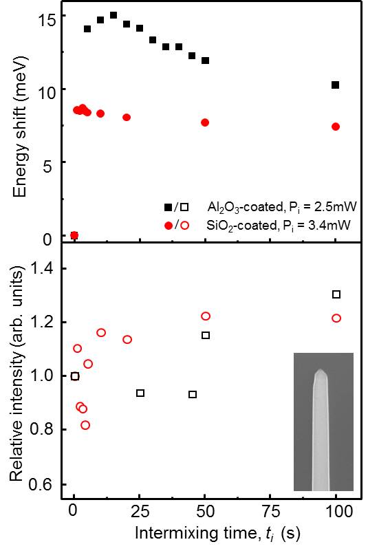
According to Equation 1, one can avoid melting the nanowire top while maintaining sufficiently high temperatures at the dot location simply by placing the dot higher in the nanowire and decreasing the laser power. Samples were grown with the quantum dot positioned m from the substrate (i.e. m higher than the devices shown in Figure 1, see Supporting Information). For these measurements, devices were prepared with either an Al2O3 or SiO2 protective coating. The energy shift and integrated intensity as a function of intermixing time are shown in Figure 4 for both types of devices. The drop in intensity observed previously is absent, in fact these devices show a modest () increase in integrated intensity after annealing. SEM images taken after intermixing (see inset, Figure 4) show no signs of nanowire melting, consistent with this behavior.
Due to the non-linear growth rate of these nanowire devicesDalacu et al. (2009), the additional core material grown to shift the quantum dots higher produces taller nanowires (7 - 8 m compared to 5 - 6 m) with a more pronounced taper. This being the case, we expect the energy shift of these Al2O3 coated devices to be different to that obtained with the shorter wires. In fact, with more defect-containing material above the quantum dot, one would expect a larger shift, as observed. We do not expect Al2O3 and SiO2 coated devices to show the same shift considering the changes to the strain environment arising from the different coatings and the role that strain plays in determining the diffusion of defects in the systemBarik et al. (2007). We also note that the power required to intermix these samples is similar to the powers which previously produced melting. The different geometry of the nanowires, and particularly the different taper, will modify the absorption profile in the wireFriedler et al. (2009); Frederiksen et al. (2017) and produce different temperatures in the nanowire for the same excitation power.
For extended anneal times both samples in Figure 4(a) exhibit a slow red-shift of the ground-state, especially pronounced for the Al2O3 coated sample. The origin of this shift is unclear but may be related to coating-mediated changes in the strain-environment. Dielectric coatings on nanowires are known to shift quantum dot emission energies due to the strain that they applyBavinck et al. (2012). For the coatings used in this study we observe a 22 nm (14 nm) red-shift (blue-shift) in the dot emission after SiO2 (Al2O3) deposition indicating that SiO2 (Al2O3) applies tensile (compressive) strain on the InP nanowire (see Supporting Information). To quantify the contribution of the observed energy shift with anneal due to a coating-mediated change in the strain environment, we have remeasured the Al2O3-coated nanowires post-anneal with the Al2O3 removed using an HF wet-etch. If the annealing process does not change the strain environment, we expect a red-shift of 14 nm. We observe slight red-shifts and even blue-shifts depending on the extent of the anneal (see Supporting Information). This behavior suggests that the strain on the InP due to the Al2O3 coating transitions from compressive to tensile during the annealing process and is consistent with the red-shift observed for extended anneals. Evidence supporting structural changes in the Al2O3 with anneal based on wet-etch rates are given in Supporting Information.
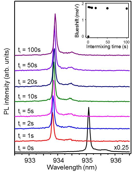
Finally, we have verified that the laser-induced intermixing approach also operates at low temperature (i.e. K). For these measurements, quantum dots emitting at nm and positioned m from the substrate were used and the protective coating was SiO2. Irradiating at the maximum HeNe laser power available (3.5 mW) did not result in any observable energy shift. To achieve high enough temperatures to promote intermixing, these samples were irradiated with a picosecond pulsed source at nm with in the range 3 to 9 mW.
PL spectra as a function of anneal time are shown in Figure 5. The intermixing shift is instantaneous on the scale of the shutter speed (500 ms) and shows a time dependence (inset) very similar to the SiO2 coated sample in Figure 4. The maximum shift obtained is meV, substantially reduced compared to the sample in Figure 4. We attribute this reduction, as above, to differences in the nanowire geometries. In particular, the nanowire diameter in this device was tailored for emission at nm (see Methods) and is much smaller than devices targeting telecom wavelengths (i.e. nm compared to nm). Consequently, the volume of defect-containing InP material above the quantum dot is significantly reduced, resulting in a smaller energy shift.
In conclusion, we have demonstrated an - technique to tune individual site-selected quantum dots using laser-induced intermixing. The observed shifts exceed the inhomogeneous broadening in our nanowire devices, thus offering a route to tune two arbitrary dots into resonance with a precision controlled through exposure time and limited by the rate of heat transfer to the substrate. We attribute the distinct saturation of the energy shift as indicative of improved material quality which has potential implications with regard to the ability to generate indistinguishable photons.
Sample Growth The InAsP/InP nanowire devices were grown using chemical beam epitaxy on patterned Fe-doped InP (111)B substrates using a combined selective-area and VLS epitaxy approachDalacu et al. (2009). The patterned substrates consisted of Au catalysts in the center of circular openings in a SiO2 mask. A two stage growth was used in which an InP nanowire core with an embedded InAsP quantum dot was grown first using growth conditions that promote VLS (i.e. axial) growth. The nanowire core was subsequently clad with an InP shell using growth conditions that promote substrate and radial growth. The shell defines the photonic waveguide necessary for the efficient collection of the quantum dot emissionFriedler et al. (2009). The diameter of the waveguide is dictated by the size of the SiO2 opening and is tailored to the dot emission wavelength (i.e. )Haffouz et al. . To provide protection against surface decomposition the devices were coated with 40 nm of Al2O3 or SiO2 deposited by atomic layer deposition (ALD) or plasma-enhanced chemical vapor deposition PECVD, respectively. For details on the device fabrication and growth, see Refs. 25, 26, and 27
Optical Spectroscopy. Photoluminescence measurements on individual nanowires were performed with the wires still attached to the (111)B InP substrate. The 4 K measurements were done in a continuous flow helium cryostat using above bandgap excitation (HeNe or Ti-Sapphire laser) through a 50X microscope objective (N.A. = 0.42) with a m spot size. The long (short) wavelength PL was collected through the same microscope objective, dispersed using a 0.32 m (0.5 m) grating spectrometer and detected using a liquid-nitrogen cooled InGaAs diode (CCD) array.
References
- Lo and Chau (1999) Lo, H.-K.; Chau, H.-F. Science 1999, 283, 2050–2056.
- Lo et al. (2012) Lo, H.-K.; Curty, M.; Qi, B. Phys. Rev. Lett. 2012, 108, 130503.
- Santori et al. (2002) Santori, C.; Fattal, D.; Vučković, J.; Solomon, G.; Yamamoto, Y. Nature 2002, 419, 594–597.
- Yoshie et al. (2001) Yoshie, T.; Scherer, A.; Chen, H.; Huffaker, D.; Deppe, D. Appl. Phys. Lett. 2001, 79, 114–116.
- Moreau et al. (2001) Moreau, E.; Gérard, J. M.; Bram, I.; Manin, L.; Thierry-Mieg, V. Appl. Phys. Lett. 2001, 79, 2865–2867.
- G. et al. (2014) G.,; Bulgarini,; Reimer, M. E.; Bavinck, M. B.; Jöns, K. D.; Dalacu, D.; Poole, P. J.; Bakkers, E. P. A. M.; Zwiller, V. Nano Lett. 2014, 7, 4102–4106.
- Aharonovich et al. (2016) Aharonovich, I.; Englund, D.; Toth, M. Nat. Photonics 2016, 10, 631–641.
- Loredo et al. (2016) Loredo, J. C. et al. Optica 2016, 3, 443.
- Wang et al. (2016) Wang, H.; Duan, Z.-C.; Li, Y.-H.; Chen, S.; Li, J.-P.; He, Y.-M.; Chen, M.-C.; He, Y.; Ding, X.; Peng, C.-Z.; Schneider, C.; Kamp, M.; Höfling, S.; Lu, C.-Y.; Pan, J.-W. Phys. Rev. Lett. 2016, 116, 213601.
- Gold et al. (2014) Gold, P.; Thoma, A.; Maier, S.; Reitzenstein, S.; Schneider, C.; Höfling, S.; Kamp, M. Phys. Rev. B 2014, 89, 035313.
- Giesz et al. (2015) Giesz, V.; Portalupi, S. L.; Grange, T.; Antón, C.; Santis, L. D.; Demory, J.; Somaschi, N.; Sagnes, I.; Lemaître, A.; Lanco, L.; Auffeves, A.; Senellart, P. Phys. Rev. B 2015, 92, 161302.
- Thoma et al. (2017) Thoma, A.; Schnauber, P.; Böhm, J.; Gschrey, M.; Schulze, J.-H.; Strittmatter, A.; S. Rodt, T. H.; Reitzenstein, S. Appl. Phys. Lett. 2017, 110, 011104.
- Reindl et al. (2017) Reindl, M.; Jöns, K. D.; Huber, D.; Schimpf, C.; Huo, Y.; Zwiller, V.; Rastelli, A.; Trotta, R. Nano Lett. 2017, 17, 4090–4095.
- Flagg et al. (2010) Flagg, E. B.; Muller, A.; Polyakov, S. V.; Ling, A.; Migdall, A.; Solomon, G. S. Phys. Rev. Lett. 2010, 104, 137401.
- Patel et al. (2010) Patel, R. B.; Bennett, A. J.; Farrer, I.; Nicoll, C. A.; Ritchie, D. A.; Shields, A. J. Nat. Photonics 2010, 4, 632.
- Haysom et al. (2000) Haysom, J. E.; Aers, G. C.; Raymond, S.; Poole, P. J. J. Appl. Phys. 2000, 88, 3090.
- Haysom et al. (2000) Haysom, J. E.; Poole, P. J.; Williams, R. L.; Raymond, S.; Aers, G. C. Solid State Commun. 2000, 116, 187.
- Dubowski et al. (2000) Dubowski, J. J.; Allen, C. N.; Fafard, S. Appl. Phys. Lett. 2000, 77, 3583.
- Girard et al. (2004) Girard, J. F.; Dion, C.; Desjardins, P.; Allen, C. N.; Poole, P. J.; Raymond, S. Appl. Phys. Lett. 2004, 84, 3382.
- Dion et al. (2006) Dion, C.; Poole, P. J.; Raymond, S.; Desjardins, P.; Schiettekatte, F. Appl. Phys. Lett. 2006, 89, 131905.
- Dion et al. (2008) Dion, C.; Desjardins, P.; Schiettekatte, F.; Chicoine, M.; Robertson, M. D.; Shtinkov, N.; Poole, P. J.; Wu, X.; Raymond, S. J. Appl. Phys. 2008, 104, 043527.
- Dion et al. (2008) Dion, C.; Desjardins, P.; Shtinkov, N.; Schiettekatte, F.; Poole, P. J.; Raymond, S. J. Appl. Phys. 2008, 103, 083526.
- Rastelli et al. (2007) Rastelli, A.; Ulhaq, A.; Kiravittaya, S.; Wang, L.; Zrenner, A.; Schmidt, O. G. Appl. Phys. Lett. 2007, 90, 073120.
- Reimer et al. (2016) Reimer, M. E.; Bulgarini, G.; Fognini, A.; Heeres, R. W.; Witek, B. J.; Versteegh, M. A. M.; Rubino, A.; Braun, T.; Kamp, M.; Höfling, S.; Dalacu, D.; Lapointe, J.; Poole, P. J.; Zwiller, V. Phys. Rev. B 2016, 93, 195316.
- Dalacu et al. (2009) Dalacu, D.; Kam, A.; Austing, D. G.; Wu, X.; Lapointe, J.; Aers, G. C.; Poole, P. J. Nanotech. 2009, 20, 395602.
- Dalacu et al. (2012) Dalacu, D.; Mnaymneh, K.; Lapointe, J.; Wu, X.; Poole, P. J.; Bulgarini, G.; Zwiller, V.; Reimer, M. E. Nano Lett. 2012, 12, 5919–5923.
- (27) Haffouz, S.; Zeuner, K. D.; Dalacu, D.; Poole, P. J.; Lapointe, J.; Poitras, D.; Mnaymneh, K.; Wu, X.; ; Couillard, M.; Korkusinski, M.; Schöll, E.; Jöns, K. D.; Zwiller, V.; Williams, R. L. DOI:10.1021/acs.nanolett.8b00550
- Chen et al. (2016) Chen, Y.; Zadeh, I. E.; Jöns, K. D.; Fognini, A.; Reimer, M. E.; Zhang, J.; Dalacu, D.; Poole, P. J.; Ding, F.; Zwiller, V.; Schmidt, O. G. Appl. Phys. Lett. 2016, 108, 182103.
- Friedler et al. (2009) Friedler, I.; Sauvan, C.; Hugonin, J. P.; Lalanne, P.; Claudon, J.; Gérard, J. M. Opt. Exp. 2009, 17, 2095.
- Barik et al. (2007) Barik, S.; Fu, L.; Tan, H. H.; Jagadish, C. Appl. Phys. Lett. 2007, 90, 243114.
- Frederiksen et al. (2017) Frederiksen, R.; Tutuncuoglu, G.; Matteini, F.; Martinez, K. L.; i Morral, A. F.; Alarcon-Llado, E. ACS Photonics 2017, 4, 2235–2241.
- Bavinck et al. (2012) Bavinck, M. B.; Zieliński, M.; Witek, B. J.; Zehender, T.; Bakkers, E. P. A. M.; Zwiller, V. Nano Lett. 2012, 12, 6206–6211.