nelsonleung@uchicago.edu
luy100@uchicago.edu††thanks: These authors contributed equally to this work.
nelsonleung@uchicago.edu
luy100@uchicago.edu
Deterministic Bidirectional Communication and Remote Entanglement Generation Between Superconducting Quantum Processors
pacs:
Valid PACS appear hereAbstract
We propose and experimentally demonstrate a simple and efficient scheme for photonic communication between two remote superconducting modules. Each module consists of a random access quantum information processor with eight-qubit multimode memory and a single flux tunable transmon. The two processor chips are connected through a one-meter long coaxial cable that is coupled to a dedicated “communication” resonator on each chip. The two communication resonators hybridize with a mode of the cable to form a dark “communication mode” that is highly immune to decay in the coaxial cable. We modulate the transmon frequency via a parametric drive to generate sideband interactions between the transmon and the communication mode. We demonstrate bidirectional single-photon transfer with a success probability exceeding 60%, and generate an entangled Bell pair with a fidelity of 79.3 0.3%.
Introduction
A practical quantum computer requires a large number of qubits working in cooperation Fowler2012SurfaceComputation , a challenging task for any quantum hardware platform. For superconducting qubits, there is an ongoing effort to integrate increasing numbers of qubits on a single chip Noroozian2012CrosstalkArrays ; Wenner2011WirebondQubits ; Chen2014FabricationCircuits ; Vesterinen2014MitigatingQubits ; Foxen2017QubitInterconnects ; Dunsworth2018ADevices ; Rosenberg20173DQubits . A promising approach to scaling up superconducting quantum computing hardware is to adopt a modular architecture Monroe2014Large-scaleInterconnects ; Brecht2016MultilayerComputing ; Chou2018DeterministicQubits in which modules are connected together via communication channels to form a quantum network. This reduces the number of qubits required on a single chip, and allows greater flexibility in reconfiguring and extending the resulting information processing system. In such an architecture, each module is capable of performing universal operations on multiple-bits, and neighboring modules are connected through photonic channels, allowing communication and entanglement generation between remote modules.
Remote entanglement between superconducting qubits has been realized probabilistically Roch2014ObservationQubits ; Narla2016RobustQubits ; Dickel2018Chip-to-chipFields . Conversely, realizing deterministic photonic communication requires releasing a single photon from one qubit and catching it with the remote qubit. In the long-distance limit, the photon emission and absorption are from a continuum density of states. In this limit, static coupling limits the maximum transfer fidelity to only 54% Stobinska2009PerfectSpace ; Wang2011EfficientMode . This limit is exceeded by dynamically tailoring the emission and absorption profiles Yin2013CatchStates ; Srinivasan2014Time-reversalTransfer ; Pechal2014Microwave-ControlledElectrodynamics ; Wenner2014CatchingEfficiency . These capabilities are presently being used to perform photonic communication between superconducting qubits connected by a transmission line within a cryostat Axline2017On-demandMemories ; Campagne-Ibarcq2017DeterministicTransitions ; Dickel2017Chip-to-chipFields ; Kurpiers2017DeterministicPhotons . In these experiments, the use of a circulator enables the finite-length transmission line to be modeled as a long line with a continuum density of states, at the cost of added transmission loss.
Here, we establish bidirectional photonic communication between two multi-qubit superconducting quantum processors through a multimodal communication channel. Rather than inserting a circulator, the multimode nature of the finite length transmission line is made manifest and exploited Jacobs2016FastNetworks . For intra-cryostat communication, the required connection coaxial cable length of 1 m or less results in a free spectral range on the order of hundreds of MHz. In this setting, the resonances of the coaxial cable form hybridized normal modes with on-chip communication resonators, and photons are transferred coherently through the discrete modes of the channel in contrast to emission/absorption through a continuum. We use parametric flux modulation of the qubit frequency to generate resonant sideband interactions between the qubit and the communication channel Beaudoin2012First-orderModulation ; Strand2013 ; Sirois2015Coherent-stateConversion ; McKay2016UniversalBus . This approach avoids the loss due to the circulator that significantly limits the communication fidelity, and enables bidirectional quantum communication.
Results
Network of two multimode modules
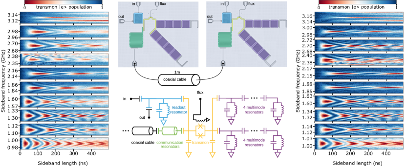
We extend the random access quantum processor module presented in Ref. Naik2017RandomElectrodynamics to allow photonic communication between two remote modules, thereby realizing a two-node quantum network. Each processor consists of an eight-qubit multimode memory comprised of two chains of four identical and strongly coupled superconducting resonators, a single flux-tunable transmon, and two additional resonators McKay2015High-ContrastQED . The first of these resonators is used for readout, and the second is coupled to the coaxial cable to enable the inter-module communication. The transmon can resonantly couple to all the resonators (readout, multimode and communication) through parametric flux modulation to realize intra-module gate operations and inter-module photonic communications. Figure 1 shows a schematic of our two modules. The readout resonators have the lowest frequencies [module 1: 5.7463 GHz; module 2: 5.7405 GHz], the communication resonators have the highest frequencies [ 7.88 GHz, see the appendix for detailed analysis of parameters] , and the eight memory mode frequencies are in the range 5.8 GHz - 7.7 GHz, spaced by 200 MHz. For the circuit design, we arranged the multimode resonators to be spatially separated from the readout and communication resonators by placing the high impedance transmon in-between, preventing Purcell loss of the multimode resonators through the low Q readout and communication resonators Houck2008ControllingQubit ; Reed2010FastQubit ; Gambetta2011SuperconductingCoupling . We operate the transmons at the static frequency of [1: 4.7685 GHz; 2: 4.7420 GHz] with an anharmonicity of [1: 109.8 MHz; 2: 109.9 MHz].
We induce resonant interactions between the transmon and an individual mode by modulating the transmon frequency via its flux bias. The modulation creates sidebands of the transmon excited state, detuned from the original resonance by the frequency of the applied flux tone. When one of these sidebands is resonant with a mode, the system experiences stimulated vacuum Rabi oscillations Naik2017RandomElectrodynamics . This process is similar to resonant vacuum Rabi oscillations Rempe1987ObservationMaser , but occur at a rate that is controlled by the modulation amplitude Strand2013 ; Beaudoin2012First-orderModulation . To illustrate the application of parametric control, we employ the following experimental sequence. First, the transmon is excited via its charge bias. Subsequently, we modulate the flux bias to create sidebands of the transmon excited state at the modulation frequency. This is repeated for different flux pulse durations and frequencies, with the population of the transmon excited state measured at the end of each sequence. When the frequency matches the detuning between the transmon and a given eigenmode, we observe full-contrast stimulated vacuum Rabi oscillations. Figure 1 shows that the transmon can selectively interact with each of the eigenmodes by choosing the appropriate modulation frequency. As previously demonstrated, this sideband interaction and rotations of the transmon are sufficient for universal operations on each set of multimode resonators Naik2017RandomElectrodynamics . Similarly, the photon transfer process between two remote qubits is initiated by switching on the sideband interactions targeting the communication resonator on each chip. As the bare frequencies of the transmon and the communication resonator are far detuned ( 3 GHz, 50 MHz), the sideband coupling scheme for photonic communication achieves a high on/off ratio.
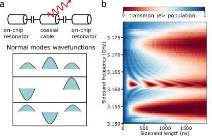
Multimode communication channel
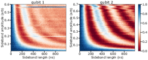
The two communication resonators are designed to have identical frequencies. They are chosen to be coplanar waveguide resonators with a large center pin and gap width to make the frequency insensitive to fabrication variations Underwood2012Low-disorderPhotons . These resonators are coupled via the one-meter long coaxial cable, where the cable can be thought of as a multimode resonator with a free spectral range of around 200 MHz. The coupling strength between the cable and the communication resonators is . The cable mode that we use for communication has a frequency that is within of the frequencies of the communication modes. Since the free spectral range of the coaxial cable is an order of magnitude larger than , we consider the cable as a single mode nearly resonant with the communication resonators. The cable and the communication resonators thus together produce three hybridized normal modes which are depicted in Figure 2. The near-degeneracy of the coaxial cable with the two communication resonators give rise to this almost equally-spaced three-mode structure, which can be seen from the three stimulated vacuum Rabi chevrons in Fig. 2 b. The center normal mode used for communication ideally has no participation in the cable mode, and as a result, its loss rate is limited by the internal quality factors of the communication resonators and small Purcell losses from neighboring cable modes. In comparison to the neighboring modes, the center normal mode couples more strongly to both qubits due to higher wavefunction participation at the communication resonators. Thus, this communication mode has both the advantages of high quality factor and high coupling rate. For any practical device, the center normal mode does have a non-zero participation in the lossy coaxial cable due to a frequency mismatch between the two on-chip communication resonators. From the measurements of previous individual test chips, the detuning between these two resonators is expected to be less than 3 MHz (), an assumption that is validated by the simulation shown in the appendix, resulting in a less than 5% of cable mode participation in the communication mode.
The coherence time of the communication mode can be characterized using protocols analogous to those for the transmon; the qubit pulses are merely sandwiched between a pair of transmon-mode iSWAP pulses to transfer the quantum state between the transmon and the mode Naik2017RandomElectrodynamics . We find ns and s, corresponding to a quality factor of about 4000. This quality factor is reasonably high, considering that it involves losses from the long lossy cable, wirebonds, solder of the SMA connector, and the copper leads of the sample holder. The two neighboring normal modes have much lower coherence times due to the higher participation of the lossy cable mode. From fitting to fig. 2b we estimate an upper bound of for these modes to be 200 ns.
Bidirectional communication
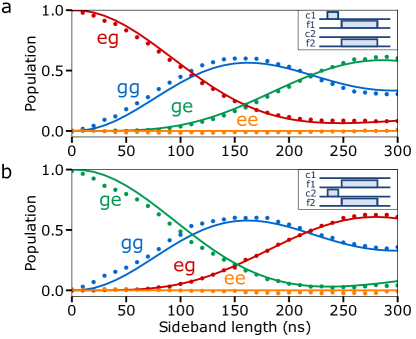
To demonstrate photonic communication between the two chips, we send a single photon from one chip to the other. First, we excite the sender qubit, then we switch on sideband interactions simultaneously on both qubits, targeting the communication channel. We send a photon in the reverse direction using the same sideband sequence but instead exciting the other qubit, thus demonstrating bidirectional photon transfer. Figure 3 shows the transmon population plotted as a function of the sideband pulse length. The master equation simulation results (solid lines) are shown along with the experimental data (dots). We are able to obtain photon transfer with a success rate of 61%. We use simultaneous square pulses for the time-envelopes of the sideband interactions. From the simulations detailed in the appendix, we found that square pulses gave superior performance for our current circuit parameters. Note that the achieved transfer fidelity exceeds 54%, the maximum fidelity for absorbing a naturally shaped emission into a continuum Stobinska2009PerfectSpace ; Wang2011EfficientMode . This demonstrates a qualitative difference in transferring via a multimode cable compared to that of releasing and catching flying photonic qubits through a continuum.
The transfer fidelity is limited by qubit dephasing and photon decay in the communication mode. Qubit 1 has a higher dephasing rate ( 700 ns) than qubit 2 ( 1.4 s). The dephasing rate of qubit 1 is comparable to the sideband coupling rate, with the result that this qubit is not able to fully release its excitation during the transfer process. Conversely, for transfer in the other direction qubit 1 is not able to receive all of the excitations. This transfer infidelity can be largely mitigated by using a fixed-frequency qubit less susceptible to the flux noise, with its coupling strength to the communication mode parametrically controlled via a tunable coupler circuit Allman2014TunableResonator ; Chen2014QubitCoupling ; Sirois2015Coherent-stateConversionb ; McKay2016UniversalBusb ; Lu2017UniversalQubitb . The remaining loss of transfer fidelity comes from the loss in the communication mode. From our numerical simulations detailed in the appendix, we estimate that the overall photon loss in both the qubits and the communication mode contribute to an infidelity of 24%, while the dephasing error of the two qubits accounts for an infidelity of 15%. The sideband coupling rate of the transmon is limited by the range over which its frequency can be parametrically tuned, resulting in a maximum effective sideband coupling to the communication resonator of 2 MHz. With improved qubit coherence time, our simulation shows that more sophisticated transfer protocols such as STIRAP Halfmann1998CoherentSO2 ; Vasilev2009OptimumPassage can be employed to boost transfer efficiency.
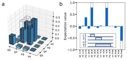
Bell state entanglement
We now entangle two qubits by creating a Bell state between the transmons on the respective chips Bell1964OnParadox . We can create such a state by first applying the gate between the excited qubit 1 and the communication mode, which generates the Bell state between them. We implement the by applying a sideband modulation pulse to qubit 1 to perform a rotation. Subsequently, we transfer the state of the communication mode to qubit 2 through the gate by applying a sideband modulation pulse to the latter to perform a rotation. Ideally this sequence prepares the Bell state shared between the two remote qubits. To minimize decoherence the sender and receiver pulses can be applied simultaneously, so long as the lengths and amplitudes of the pulses are adjusted appropriately. Choosing qubit 1 as the sender and using square pulses, we found — both in our simulation and in the experiment — that maximal fidelity was obtained by setting both pulses at the same coupling rate and the length of the receiver pulse to be slightly longer than twice that of the sender. The resulting Bell state has a fidelity of 79.3 0.3%. We obtained the density matrix using quantum state tomography with an over-complete set of measurements complemented with the maximum likelihood method James2001MeasurementQubits . It can be inferred from the data that the fidelity is almost equally limited by photon decay in the cable and the qubit dephasing errors. We also note that the Bell state fidelity is significantly higher than the success probability we achieved for photon transfer. Likely explanations for this is that qubit 1 is actively involved in the process for only half the duration of the protocol and there is less excitation in the cable over the duration of the protocol. The process is thus less sensitive to the dephasing noise in the qubit and decay loss in the cable.
Conclusion
We have built upon the random access quantum information processor previously presented in Ref. Naik2017RandomElectrodynamics , so as to realize photonic communication between two remote modules, a first step in realizing a modular network. The sideband modulation of the transmon qubit in each module can be applied to implement local operations on the multimode resonators and to perform photon transfer between the two modules. The multimode characteristic of the communication channel (a coaxial cable) is enabled by the absence of a circulator. This mode structure results in normal modes that are superpositions of a mode of the inter-module communication cable and the on-chip resonators. One of the these normal modes is “dark” to the coaxial cable mode, thus avoiding much of the cable loss and allowing for high fidelity photon transfer. We characterized our system by performing single photon transfer with 61% fidelity and Bell-state preparation with 79.3% fidelity. These fidelities can be increased by improving the qubit coherence time and the strength of the coupling to the communication channel. Future work will include implementing more sophisticated photon transfer protocols (e.g. STIRAP), applying heralding protocols to protect against photon transmission error, implementing local gates on memory modes in conjunction with photonic communication to facilitate large-scale computation, and integrating the present architecture with high-quality-factor 3D superconducting cavities Reagor2013ReachingCavities .
Data availability
Data available on request from authors.
References
- (1) Fowler, A. G., Mariantoni, M., Martinis, J. M. & Cleland, A. N. Surface codes: Towards practical large-scale quantum computation. Physical Review A 86, 032324 (2012).
- (2) Noroozian, O., Day, P. K., Eom, B. H., Leduc, H. G. & Zmuidzinas, J. Crosstalk Reduction for Superconducting Microwave Resonator Arrays. IEEE Transactions on Microwave Theory and Techniques 60, 1235–1243 (2012).
- (3) Wenner, J. et al. Wirebond crosstalk and cavity modes in large chip mounts for superconducting qubits. Superconductor Science and Technology 24, 065001 (2011).
- (4) Chen, Z. et al. Fabrication and characterization of aluminum airbridges for superconducting microwave circuits. Applied Physics Letters 104, 052602 (2014).
- (5) Vesterinen, V., Saira, O. P., Bruno, A. & DiCarlo, L. Mitigating information leakage in a crowded spectrum of weakly anharmonic qubits (2014). eprint arXiv:1405.0450.
- (6) Foxen, B. et al. Qubit compatible superconducting interconnects (2017). eprint arXiv:1708.04270.
- (7) Dunsworth, A. et al. A method for building low loss multi-layer wiring for superconducting microwave devices. Applied Physics Letters 112, 063502 (2018).
- (8) Rosenberg, D. et al. 3D integrated superconducting qubits. npj Quantum Information 3, 42 (2017).
- (9) Monroe, C. et al. Large-scale modular quantum-computer architecture with atomic memory and photonic interconnects. Physical Review A 89, 022317 (2014).
- (10) Brecht, T. et al. Multilayer microwave integrated quantum circuits for scalable quantum computing. npj Quantum Information 2, 16002 (2016).
- (11) Chou, K. S. et al. Deterministic teleportation of a quantum gate between two logical qubits (2018). eprint arXiv:1801.05283.
- (12) Roch, N. et al. Observation of Measurement-Induced Entanglement and Quantum Trajectories of Remote Superconducting Qubits. Physical Review Letters 112, 170501 (2014).
- (13) Narla, A. et al. Robust Concurrent Remote Entanglement Between Two Superconducting Qubits. Physical Review X 6, 031036 (2016).
- (14) Dickel, C. et al. Chip-to-chip entanglement of transmon qubits using engineered measurement fields. Physical Review B 97, 064508 (2018).
- (15) Stobińska, M., Alber, G. & Leuchs, G. Perfect excitation of a matter qubit by a single photon in free space. EPL (Europhysics Letters) 86, 14007 (2009).
- (16) Wang, Y., Minář, J., Sheridan, L. & Scarani, V. Efficient excitation of a two-level atom by a single photon in a propagating mode. Physical Review A 83, 063842 (2011).
- (17) Yin, Y. et al. Catch and Release of Microwave Photon States. Physical Review Letters 110, 107001 (2013).
- (18) Srinivasan, S. J. et al. Time-reversal symmetrization of spontaneous emission for quantum state transfer. Physical Review A 89, 033857 (2014).
- (19) Pechal, M. et al. Microwave-Controlled Generation of Shaped Single Photons in Circuit Quantum Electrodynamics. Physical Review X 4, 041010 (2014).
- (20) Wenner, J. et al. Catching Time-Reversed Microwave Coherent State Photons with 99.4% Absorption Efficiency. Physical Review Letters 112, 210501 (2014).
- (21) Axline, C. et al. On-demand quantum state transfer and entanglement between remote microwave cavity memories (2017). eprint arXiv:1712.05832.
- (22) Campagne-Ibarcq, P. et al. Deterministic remote entanglement of superconducting circuits through microwave two-photon transitions (2017). eprint arXiv:1712.05854.
- (23) Dickel, C. et al. Chip-to-chip entanglement of transmon qubits using engineered measurement fields (2017). eprint arXiv:1712.06141.
- (24) Kurpiers, P. et al. Deterministic Quantum State Transfer and Generation of Remote Entanglement using Microwave Photons (2017). eprint arXiv:1712.08593.
- (25) Jacobs, K. et al. Fast quantum communication in linear networks. EPL (Europhysics Letters) 114, 40007 (2016).
- (26) Beaudoin, F., da Silva, M. P., Dutton, Z. & Blais, A. First-order sidebands in circuit QED using qubit frequency modulation. Physical Review A 86, 022305 (2012).
- (27) Strand, J. D. et al. First-order sideband transitions with flux-driven asymmetric transmon qubits. Phys. Rev. B 87, 220505 (2013).
- (28) Sirois, A. J. et al. Coherent-state storage and retrieval between superconducting cavities using parametric frequency conversion. Applied Physics Letters 106, 172603 (2015).
- (29) McKay, D. C. et al. Universal Gate for Fixed-Frequency Qubits via a Tunable Bus. Physical Review Applied 6, 064007 (2016).
- (30) Naik, R. K. et al. Random access quantum information processors using multimode circuit quantum electrodynamics. Nature Communications 8, 1904 (2017).
- (31) McKay, D. C., Naik, R., Reinhold, P., Bishop, L. S. & Schuster, D. I. High-Contrast Qubit Interactions Using Multimode Cavity QED. Physical Review Letters 114, 080501 (2015).
- (32) Houck, A. A. et al. Controlling the Spontaneous Emission of a Superconducting Transmon Qubit. Physical Review Letters 101, 080502 (2008).
- (33) Reed, M. D. et al. Fast reset and suppressing spontaneous emission of a superconducting qubit. Applied Physics Letters 96, 203110 (2010).
- (34) Gambetta, J. M., Houck, A. A. & Blais, A. Superconducting Qubit with Purcell Protection and Tunable Coupling. Physical Review Letters 106, 030502 (2011).
- (35) Rempe, G., Walther, H. & Klein, N. Observation of quantum collapse and revival in a one-atom maser. Physical Review Letters 58, 353–356 (1987).
- (36) Underwood, D. L., Shanks, W. E., Koch, J. & Houck, A. A. Low-disorder microwave cavity lattices for quantum simulation with photons. Physical Review A 86 (2012).
- (37) Allman, M. et al. Tunable Resonant and Nonresonant Interactions between a Phase Qubit and L C Resonator. Physical Review Letters 112, 123601 (2014).
- (38) Chen, Y. et al. Qubit Architecture with High Coherence and Fast Tunable Coupling. Physical Review Letters 113, 220502 (2014).
- (39) Sirois, A. J. et al. Coherent-state storage and retrieval between superconducting cavities using parametric frequency conversion. Applied Physics Letters 106, 172603 (2015).
- (40) McKay, D. C. et al. Universal Gate for Fixed-Frequency Qubits via a Tunable Bus. Physical Review Applied 6, 064007 (2016).
- (41) Lu, Y. et al. Universal Stabilization of a Parametrically Coupled Qubit. Physical Review Letters 119, 150502 (2017).
- (42) Halfmann, T. & Bergmann, K. Coherent population transfer and dark resonances in SO2. The Journal of Chemical Physics 104, 7068 (1998).
- (43) Vasilev, G. S., Kuhn, A. & Vitanov, N. V. Optimum pulse shapes for stimulated Raman adiabatic passage. Physical Review A 80, 013417 (2009).
- (44) Bell, J. On the Einstein-Podolsky-Rosen paradox. Physics 1, 195–200 (1964).
- (45) James, D. F. V., Kwiat, P. G., Munro, W. J. & White, A. G. Measurement of qubits. Physical Review A 64, 052312 (2001).
- (46) Reagor, M. et al. Reaching 10 ms single photon lifetimes for superconducting aluminum cavities. Applied Physics Letters 102, 192604 (2013).
- (47) Wallraff, A. et al. Approaching Unit Visibility for Control of a Superconducting Qubit with Dispersive Readout. Physical Review Letters 95, 060501 (2005).
- (48) Chow, J. M. et al. Detecting highly entangled states with a joint qubit readout. Physical Review A 81, 062325 (2010).
- (49) Leung, N., Abdelhafez, M., Koch, J. & Schuster, D. Speedup for quantum optimal control from automatic differentiation based on graphics processing units. Physical Review A 95, 042318 (2017).
Acknowledgements.
The authors thank R. Cook, Y. Zhong, and A. A. Clerk for useful discussions, and A. Oriani for support with cryogenic facilities. This material is based upon work supported by the Army Research Office under (W911NF-15-2-0058). The views and conclusions contained in this document are those of the authors and should not be interpreted as representing the official policies, either expressed or implied, of the Army Research Laboratory or the U.S. Government. The U.S. Government is authorized to reproduce and distribute reprints for Government purposes notwithstanding any copyright notation herein. Research was also supported by the U. S. Department of Defense under DOD contract H98230-15-C0453. This work was partially supported by the University of Chicago Materials Research Science and Engineering Center, which is funded by the National Science Foundation under Award No. DMR-1420709. This work made use of the Pritzker Nanofabrication Facility of the Institute for Molecular Engineering at the University of Chicago, which receives support from SHyNE, a node of the National Science Foundation’s National Nanotechnology Coordinated Infrastructure (NSF NNCI-1542205). We gratefully acknowledge support from the David and Lucile Packard Foundation.Author contributions
N.L., Y.L designed and fabricated the device, designed the experimental protocols, performed the experiments, and analyzed the data. K.J. provided theoretical support. S.C., R.N., N.E., R.M provided fabrication and experimental support. All authors co-wrote the paper.
Competing financial interests
The authors declare no competing financial interests.
Appendix A Cryogenic setup and control instrumentation
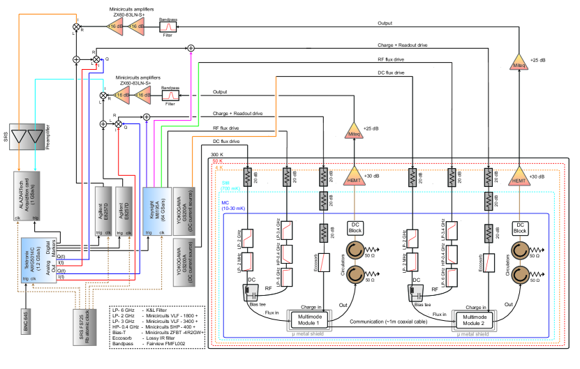
The device is heat sunk via an OFHC copper post to the base stage of a Bluefors dilution refrigerator (10-30 mK). The sample is surrounded by a can containing two layers of -metal shielding and a layer of lead shielding, thermally anchored using an inner close fit copper shim sheet, attached to the copper can lid. The schematic of the cryogenic setup, control instrumentation, and the wiring of the device is shown if Supplementary Figure 5. Each device is connected to the rest of the setup through three ports: a charge port that applies qubit and readout drive tones, a flux port for shifting the qubit frequency using a DC-flux bias current and for applying RF sideband flux pulses, and an output port for measuring the transmission from the readout resonator. The readout pulses are generated by mixing a local oscillator tone (generated from an Agilent 8257D RF signal generator), with pulses generated by a Tektronix AWG5014C arbitrary waveform generator (TEK) with a sampling rate of 1.2 GSa/s, using an IQ-Mixer (MARQI MLIQ0218). The charge drive pulses are generated with Keysight M8195A arbitrary waveform generator by direct synthesis, and subsequently combined with the readout drive pulse. The combined signals are sent to the device, after being attenuated a total of 60 dB in the dilution fridge, using attenuators thermalized to the 4K (20 dB), still (20 dB) and base stages (20 dB). The charge drive line also includes a lossy ECCOSORB CR-117 filter to block IR radiation, and a low-pass filter with a sharp roll-off at 6 GHz, both thermalized to the base stage. The flux-modulation pulses are also directly synthesized by the Keysight M8195A arbitrary waveform generator and attenuated by dB at the 4 K stage, and bandpass filtered to within a band of 400 MHz - 3.4 GHz at the base stage, using the filters indicated in the schematic. The DC flux bias current is generated by a YOKOGAWA GS200 low-noise current source, attenuated by 20 dB at the 4 K stage, and low-pass filtered down to a bandwidth of 1.9 MHz. The DC flux bias current is combined with the flux-modulation pulses at a bias tee thermalized at the base stage. The state of the transmon is measured using the transmission of the readout resonator, through the dispersive circuit QED readout scheme Wallraff2005ApproachingReadout . The transmitted signal from the readout resonator is passed through a set of cryogenic circulators (thermalized at the base stage) and amplified using a HEMT amplifier (thermalized at the 4 K stage). Once out of the fridge, the signal is filtered (narrow bandpass filter around the readout frequency) and further amplified. The amplitude and phase of the resonator transmission signal are obtained through a heterodyne measurement, with the transmitted signal demodulated using an IQ mixer and a local oscillator at the readout resonator frequency. The heterodyne signal is amplified (SRS preamplifier) and recorded using a fast ADC card (ALAZARtech).
Appendix B Device Hamiltonian
Without connecting to the coaxial cable, the Hamiltonian of the i-th (i=1,2) circuit can be modeled by
| (1) |
where , , and stand for the annihilation operators of the flux-tunable qubit, the readout resonator, the communication cavity and the m-th multimode on the i-th chip. The communication cavities of the two chips are of identical coplanar waveguide resonator design with large center pin and gap width, leading to approximately the same resonant frequency and the same coupling strength to the coaxial cable mode ,
| (2) |
2 can be directly diagonalized, yielding three normal modes , and ,
| (3) |
where
| (4) |
and
| (5) |
Here stands for the deviation of the cable mode frequency from the communication resonator frequency, i.e. , and . The normal mode frequencies relative to the qubit frequency can be readily obtained from Fig. 2.b, so that and can be calculated from Eq. 3 and 4. Eq. 1 and 5 together give the renormalized coupling strengths between the qubit and these normal modes,
| (6) |
It is worth noting that the center normal mode, , is selected to be our communication channel mode in the experiment, for two obvious reasons: it contains only the two resonator modes with no convolution with the cable mode, as seen in Eq. 5, thus highly immune to the photon loss of the cable. Eq. 6 shows that it also couples more strongly to the qubit comparing to the other two normal modes, which also agrees well with Fig. 2.b where the center chevron has the fastest oscillation.
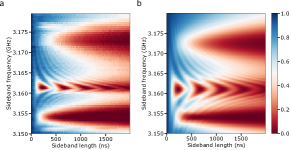
Fitting Eq. 4 to Fig. 2b, we obtain MHz and MHz, from which we can numerically reproduce the chevron patterns observed in the experiment (Fig.6).
Here we list the relevant circuit parameters in the following table:
| sample 1 | sample 2 | |
|---|---|---|
| static: 4.7685 GHz; range: 3.0 - 5.9 GHz | static: 4.7420 GHz; range: 3.5 - 5.5 GHz | |
| 109.8 MHz | 109.9 MHz | |
| 5.7463 GHz | 5.7405 GHz | |
| 7.88 GHz | 7.88 GHz | |
| 5.9 - 7.6 GHz | 5.9 - 7.6 GHz | |
| 10.1 s | 7.9 s | |
| 0.7 s | 1.4 s |
Appendix C Sideband interaction and calibrations
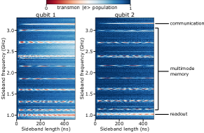
In these scans, we can clearly identify ten chevron patterns corresponding to one readout resonator, eight multimode memory resonators, and one communication resonator. The crosstalk at sideband frequency 2.4 GHz corresponds to directly driving the g-e transition at the half of this frequency. The clean chevron patterns indicate that our transmons are free from spurious crosstalks. Compared to the segmented scans in the main text, these sideband scans are taken at higher amplitude to broaden the chevron patterns for better visualization. The chevron patterns also show with faster oscillations and slightly higher frequency due to DC-offset, described in the next section.
The essential ingredient of photonic communication for our devices is the flux sideband interaction. It is therefore important to calibrate the sideband interactions well on both devices for obtaining high fidelity photonic communication. For our devices, this involves using the correct amplitude, frequency and timing of the sideband interactions. This section describes our calibration protocols for these parameters.
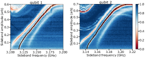
First, we run a 2D sweep (sideband amplitude and sideband frequency) of stimulated vacuum rabi around the communication mode frequencies. The main feature in figure 8 shows a clear pattern of three resonances, corresponds to the three hybridized normal modes of the communication channel. From the data, it is obvious that the resonance frequencies are dependent on the sideband amplitudes. The effect originated from the non-linear flux-frequency relation of the transmon, causing a shift (DC-offset) of the qubit frequency during the flux modulation. By doing a finer scan around the resonance frequency, we calibrated the on-resonance frequency of each sideband amplitude with an accuracy of 100 kHz.
With the calibrated frequencies, we sweep the sideband length with a range of sideband amplitudes and obtain stimulated vacuum Rabi oscillation. The experimental data is displayed in figure 9. As expected, a higher sideband amplitude implies a higher effective coupling rate. Using this data, we obtained the effective qubit dissipation parameters during the sideband coupling. These dissipation parameters are subsequently being applied in master equation simulation of photon transfer and Bell entanglement generation.
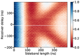
Lastly, we calibrated the timing of the two flux sideband pulses. Due to slightly different travel path length of flux line control from AWG to sample, we expect a slightly different timing between the two flux sideband pulses. Since the simultaneity of two flux sideband pulses is essential for high fidelity transfer, it is important to calibrate this systematic error. The experiment was conducted with two equal length sideband pulses but sweeping the software delay between two pulses. Here, a negative receiver delay means the sender qubit (qubit 1) sideband pulse starts before the receiver qubit (qubit 2) sideband pulse. Figure 10 shows the population of the sender qubit with sweeping parameters of two sideband length and receiver delay. The center of the “K" pattern corresponds to the scenario where the photon is maximally captured by the receiver qubit. We obtained the “K" pattern as symmetric around receiver delay time of -10 ns, indicating the flux sideband pulse of the receiver qubit (qubit 2) lags the flux sideband pulse of the sender qubit (qubit 1). As a sanity check, we switched the role of sender and receiver qubit, such that sender is qubit 2 and receiver is qubit 1. In such case, we found that the pattern is symmetric around receiver delay time of +10 ns. This confirms our conclusion that indeed the qubit 2 lags the flux sideband pulse of qubit 1 due to a delay in the lines.
Appendix D Master equation simulation
In order to calculate the communication processes between the remote qubits using master equation simulations, we first write out the circuit Hamiltonian under flux modulations, based on Eq. 16, as
| (7) |
where stand for the three normal mode and their coupling strengths to the two transmon qubits. Assuming weak flux modulation with , and under the rotating frame transformation exp, Eq. 7 can be rewritten as
| (8) |
Here stands for the Bessel function of the first kind of the first order, and all the fast-oscillating terms have been abandoned. With the flux-modulation frequencies being , and applying the two-level-approximation for the qubits, we find the "transfer Hamiltonian" as
| (9) |
where and are the two lossy “bright” normal mode, and is the “dark" communication channel mode. Plugging this into the master equation,
| (10) |
we are able to simulate the bidirectional photon transfer experiment (Fig. 3) and the remote entanglement experiment (Fig. 4).
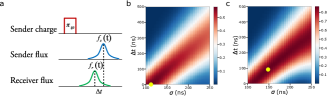
Simultaneous square sideband pulses are adopted in both the photon transfer and Bel state creation experiment to achieve the shortest pulse time possible, as is shown in fig. 3 and 4. However, there is a possibility that better fidelities could be acquired through further minimizing the photon loss in the communication mode, by making use of adiabatic protocols in a manner akin to the stimulated Raman adiabatic passage (STIRAP). A typical STIRAP protocol has a pulse sequence shown in fig. 11a, where after the excitation of the sender qubit, the receiving pulse turns on first, and slowly ramps down together with the ramping up of the sending pulse. When the ramping of the pulses are done adiabatically w.r.t the gap between the communication mode and the qubit modes, the transfer could be completed without inducing the communication mode population, and is therefore immune to the photon loss in the communication mode. However, this comes at the cost of much longer transfer time, which introduces more loss from the qubits.
For simplicity we model the sender and receiver pulses as two Gaussian pulses with the same maximum amplitude as the square pulse scheme used in our experiment. In the time domain, the two pulses are set to be
| (11) |
The fidelity yielded by this protocol is calculated as a function of both the pulse width and the delay time , via master equation simulation with real circuit parameters. Fig. 11b shows that a maximum fidelity of 56% is achieved when two Gaussian pulses with us overlap each other, which indicates that non-adiabatic transfer with shortest time is favorable in our current parameter regime. This also justifies our choice of the simultaneous square pulse scheme which is the fastest in all non-adiabatic schemes. In contrast, if the coherence of the qubit is improved to us and us, the same simulation results in a maximum fidelity of 85% at delay time (fig. 11c) that is higher than the simultaneous square pulse fidelity of 82%, proving the usefulness of the adiabatic protocol for future improvements.
Appendix E Readout and state tomography
To measure the two-qubit state, we record the homodyne voltage for each qubit from every run. For example, run of the experiment would result in a 4D heterodyne voltage values (, , , ). These voltages are random numbers generated from a specific distribution corresponding to state projection and experimental noise. To measure the population in the four two-qubit basis states: we construct the histograms for these states by applying pulses to the qubits. These histograms approximate the probability distribution for measuring a given voltage pair when the system is in a given basis state.
We employed logistic regression for classification of the two-qubit states. By setting decision thresholds for maximizing the classification accuracy for the two-qubit basis states according to the voltage distribution, we obtain a confusion matrix representing the correct and incorrect identification of basis state. For an unknown density matrix we construct the classification distribution for from N measurements, and project onto the basis states by applying the inverse of the calculated confusion matrix.
We perform state tomography using the standard method by calculating the linear estimator,
| (12) |
To calculate the term we apply a unitary operator to prior to measurement. For two-qubits, there are nine required measurements corresponding to the following unitary operators, .
This simple linear estimator method can return unphysical results because it projects onto the space of all Hermitian matrices with Trace 1. However a physical density matrix must also be positive semi-definite. Following the maximum likelihood protocol outlined in McKay2015High-ContrastQED ; James2001MeasurementQubits , we estimate the most likely physical density matrix by minimizing the function,
| (13) |
, where are the set of applied tomography pulses, is the basis state, is the measured probability, and is a physical density matrix satisfying the physical constraints. The starting guess for the minimization is the density matrix estimated from the linear estimator with all negative eigenvalues set to zero. To form a over-complete set for a total of 17 tomography measurements, we also measure the negative pulse set Chow2010DetectingReadout .
Appendix F Online Gaussian process for Bell state optimization
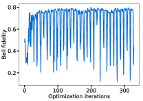
For two square pulses, there are in total 6 parameters (amplitude, frequency, and duration of each square pulse). The linear interpolation calibration of the DC offsets relates the amplitude and frequency parameters, thus resulting in 4 parameters to be optimized. All the parameters are fairly dependent on each other in the process of simultaneous transfer, meaning all 4 parameters have to be optimized together. Exhaustive search is quite forbidden even with just 4 parameters. Therefore, we employed optimization techniques, in particular, the Gaussian process to assist in optimizing Bell state creation. We employed an online optimization directly applied to the experimental device. In each iteration, the Gaussian process model proposes 8 candidate solution (1 obtained from L-BFGS-B optimization on the Gaussian model, and 7 obtained from random sampling filtered with the best model prediction), and we also test 2 candidate solution from pure random sampling to improve parameter space exploration. Figure 12 shows the optimization trajectory of Bell state creation. The model quickly starts to converge, and after some time we obtained Bell state with a fidelity close to 80%. Since only half of the excitation is being transmitted in the process, the transmission is less likely to be lost. We are able to obtain bell state creation with a fidelity higher than single photon transfer. During the optimization, we clipped the value of density matrix to a maximum of 0.5 for the calculation of fidelity. Without doing so, we found our numerical optimization results bias towards a higher excited population ( 0.5) of the sender qubit, where ideally one would expect the excited population to be 0.5. This artifact is likely due to the inner product definition of the fidelity, where 0.5 excited population actually increases part of the inner products. We also took the absolute value of the resulting density matrix. This process optimized the Bell state up to a local qubit phase. To recover the target Bell state, we used the transfer parameters obtained from the optimizer and applied local phase advancement on one of the qubits. We repeated the Bell state creation experiment for 10+ times to obtain a statistics on the error of the Bell state fidelity. The resulted Bell state fidelity with this procedure was 79.3% 0.3%. The online optimization with Gaussian process works reasonably well even we started with random initial parameters for the two square pulses. For arbitrarily shaped pulses, the high-dimensionality would necessarily require one to employ a model-based offline quantum optimal control Leung2017SpeedupUnits to facilitate the optimization process.