The critical role of substrate disorder in valley splitting in Si quantum wells
Abstract
Atomic-scale disorder at the top interface of a Si quantum well is known to suppress the valley splitting. Such disorder may be inherited from the underlying substrate and relaxed buffer growth, but can also arise at the top quantum well interface due to the random SiGe alloy. Here, we perform activation energy (transport) measurements in the quantum Hall regime to determine the source of the disorder affecting the valley splitting. We consider three Si/SiGe heterostructures with nominally identical substrates but different barriers at the top of the quantum well, including two samples with pure-Ge interfaces. For all three samples, we observe a surprisingly strong and universal dependence of the valley splitting on the electron density () over the entire experimental range (=30-200 eV). We interpret these results via tight binding theory, arguing that the underlying valley physics is determined mainly by disorder arising from the substrate and relaxed buffer growth.
Gate-defined quantum dots in Si are attractive candidates for quantum bits (qubits), because of their weak spin-orbit coupling, natural abundance of nuclear-spin-zero 28Si, and compatibility with industrial scale fabrication techniques Zwanenburg et al. (2013). However, Si qubits are affected by the conduction band valley degeneracy, which is twofold for devices formed in Si/SiGe quantum wells or at Si-MOS interfaces Ando et al. (1982); Schäffler (1997). The remaining degeneracy is lifted by a sharp quantum well interface. The energy difference between these levels, known as the valley splitting, depends on details of the interface, including atomic-scale disorder, as well as the vertical electric field Ando (1979); Friesen et al. (2006, 2007); Kharche et al. (2007). For several types of silicon spin qubits, including single-spin Veldhorst et al. (2015); Yoneda et al. (2018); Zajac et al. (2018); Watson et al. (2018), singlet-triplet Petta et al. (2005); Maune et al. (2012); Wu et al. (2014); Nichol et al. (2017), and exchange-only Gaudreau et al. (2011); Medford et al. (2013); Eng et al. (2015), the valley splitting should be large enough that only the lowest valley state is accessible during preparation, manipulation, and readout. Furthermore, valley splitting sets the energy scale for silicon-based quantum dot hybrid qubits Kim et al. (2014, 2015); Schoenfield et al. (2017); Thorgrimsson et al. (2017), and should be in a range that is appropriate for AC gating (10 GHz). For all qubit schemes, scalability will be enhanced when the valley splitting is as predictable and repeatable as possible.
Large valley splittings have been relatively easy to achieve in Si-MOS quantum dots, due to the combination of strong, tunable electric fields and abrupt SiO2 interfaces Yang et al. (2013); Gamble et al. (2016), and in donor-based qubits it arises naturally from the strong three-dimensional confinement Pla et al. (2012); Harvey-Collard et al. (2017); Broome et al. (2018). In Si/SiGe heterostructures, valley splittings tend to be smaller, making more important any variations in the valley splitting that can arise, for example, from variability in the sharpness and disorder of quantum well interfaces; experimental measurements reveal valley splittings ranging from tens to hundreds of eV Weitz et al. (1996); Koester et al. (1997); Lai et al. (2006); Goswami et al. (2007); Shi et al. (2011, 2014); Mi et al. (2015), 1-2 orders of magnitude below theoretical predictions for ideal quantum wells Boykin et al. (2004). Recent theoretical work predicts that specific alternating layers of pure Si and pure Ge at the quantum well top interface may significantly enhance the valley splitting Zhang et al. (2013). However, the added complexity could increase the atomic-scale disorder. To minimize such effects, it is interesting to consider a simplified structure, reflecting the common element in each of the proposed heterostructures: a thin, pure-Ge layer at the top of the quantum well. As an added benefit, this structure has no alloy disorder in the active region, which could also suppress the valley splitting Kharche et al. (2007).
Here we report the growth of heterostructures with a thin, pure-Ge layer at the top of the quantum well. Structural characterization by scanning transmission electron microscopy (STEM) reveals this layer to be approximately 5 monolayers thick. We report electronic transport measurements on three Hall bars, one each from two different heterostructures with such a thin Ge layer, and one from a conventional Si/SiGe heterostructure used as a control. We find the electron mobility at a density of 41011cm-2 in these samples is slightly lower in the presence of the Ge layer (56,000 and 70,000 cm2/Vs, compared to 100,000 cm2/Vs for the control sample). Magnetotransport measurements performed on all three samples reveal well developed Shubnikov-de Haas oscillations and integer quantum Hall plateaus. We report activation energy measurements for magnetic fields corresponding to filling factors =3 and =5, for electron densities ranging from 2.01011 to 5.51011 cm-2. These measurements reveal energy gaps, corresponding to the valley splitting, which vary from a minimum of 30 eV up to 200 eV, with the latter value attained for a sample with a pure Ge layer, at an electron density of =510cm-2 and filling factor =3. While the relatively small differences in the measured mobilities and valley splittings between the studied samples at fixed electron density can be attributed to heterostructure modulations and the presence or absence of alloy disorder at the top of the quantum well, we observe a much stronger dependence of the valley splitting on the electron density and the corresponding vertical electric field, which is consistent across all three samples, including the control. Tight binding theory, including both the experimentally applied electric field and interface disorder in the form of atomic steps, is able to explain this steep dependence on density. Based on the combination of these theoretical results and the experimental observations, we propose that disorder in the underlying substrate and relaxed buffer layer, which is nominally identical for all three samples, is a dominant contributor to the valley splitting and its dependence on electron density.
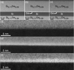
All three samples are grown by CVD on commercially linearly-graded SiGe alloy with a final 2 m Si0.71Ge0.29 layer that is chemo-mechanically polished. Before the final CVD growth, these virtual substrates are ultrasonically degreased in acetone, then methanol, then rinsed in DI water. The native oxide is stripped in HF, DI rinsed, and then regrown in a UV-Ozone cleaner; this process is repeated once more. The samples are then Piranha cleaned, DI rinsed, and SC1 cleaned. After a final 5 minute DI rinse, the samples are dipped in 10% HF for 20 seconds and loaded immediately into an LPCVD reactor where they are flash heated to 825∘C while silane and germane are flowing, then the temperature is reduced to the final 600∘C level. A 580 nm 29% Ge alloy layer is deposited before growing the final well. For Sample A, the control, a conventional Si/SiGe heterostructure is grown. Samples B and C include a 1 nm thick interfacial layer of Ge above the Si quantum well. All three heterostructures have 13 nm Si quantum wells, followed by 34 nm barriers of Si0.71Ge0.29 (A) or Ge/Si0.71Ge0.29 (B,C), and 0.5 nm Si capping layers. The composition of each layer is set by the flow rates of the precursor gases: silane for Si and germane for Ge. For samples A and B, the growth is done continuously, at a constant temperature of 600∘C, ensuring that there is always active gas at the growth surface. For sample C, at the top of the quantum well we lower the sample temperature to 400∘C to pause the growth while the reactive gas is changed from silane to germane, potentially yielding a more chemically abrupt interface with a modified disorder morphology. We then exchange the Si and Ge precursors, while the sample is cold, and raise the temperature back to 600∘C to resume the growth of the Ge/Si0.71Ge0.29 barrier.
Figure 1 shows high-angle annular dark-field images of the three samples, taken with a scanning transmission electron microscope (STEM). The images confirm that samples B and C have a high concentration of Ge extending 1 nm above the Si quantum well, corresponding to 5 monolayers of material. The higher resolution images in Figs. 1(d)-1(f) suggest that all the samples have quite abrupt top quantum well interfaces; any differences in the abruptness are beyond the resolution of the STEM.
The undoped heterostructures were patterned with Hall bars of dimension 20 200 m. Ti/Au gates were evaporated on top of a 95 nm thick atomic layer deposition film of Al2O3, enabling in-situ tuning of the electron density. The mobilities of the samples at a density of 41011 cm-2 are 100,000 for Sample A, 70,000 for Sample B, and 56,000 for Sample C, all in units of cm2/Vs. While the samples with Ge at the quantum well top interface have lower mobility, for all three samples the mobilities are consistent with previous demonstrations of quantum dot devices in Si/SiGe heterostructures Simmons et al. (2009); Wang et al. (2013).
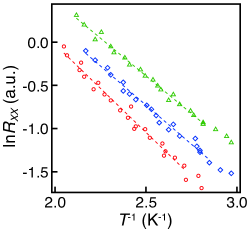
In Fig. 2, we report the magnetoresistance of all three samples in a cryostat at base temperature (50 mK). Shubnikov-de Haas minima in occur when the Fermi level lies in the Landau level gaps with odd-numbered filling factors (), corresponding to valley splittings Schäffler (1997). We measure the temperature dependence of by fixing the magnetic field, heating the sample to 250 mK, and allowing it to cool slowly while measuring . A typical data set is shown in Fig. 2(d). In the activated regime, the minima follow an Arrhenius scaling, Weitz et al. (1996), allowing us to determine the mobility gap corresponding to valley splitting (see supplementary material). The primary source of uncertainty arises from the choice of the temperature range for the fitting. At lower temperatures, is dominated by hopping conduction rather than activation, yielding a nonlinear Arrhenius plot Ebert et al. (1983). A departure from linearity also occurs at high temperatures, as the minima begin to shift in position and disappear Usher et al. (1990). To exclude these effects, we perform the fits over ranges that appear linear by eye on Arrhenius plots, and we estimate the uncertainty in the slope by varying the fitting range until it includes clearly nonlinear regions.
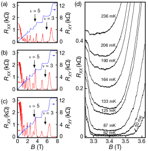
As a control experiment, and to compare the mobility gap to an expected single particle gap, we apply this method to the Zeeman splitting of the =6 Landau level. We obtain a gap from the Arrhenius fits corresponding to Landé -factors of for sample A, for sample B, and for sample C, close to the expected single particle value of =2 for Si and providing an indication of the difference between the single particle gap and the mobility gap in these samples Prange and Girvin (1990).
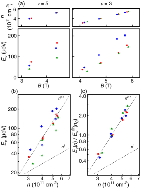
Mobility gaps corresponding to valley excitations are reported in the lower two panels of Fig. 3(a), which show the extracted gaps for =5 and 3. While the largest gap occurs for sample C, which has enhanced Ge concentration at the top of the well, the presence or absence of such a single Ge layer does not have a dramatic effect on the valley splitting gaps we measure here, indicating that alloy disorder does not play an important role in determining the valley splitting in these samples. In fact, all three samples reveal energy gaps that increase quite similarly with increasing perpendicular magnetic field. One reason for this dependence is that larger magnetic fields cause electrons to occupy smaller orbits, thus mitigating the suppression of valley splitting due to interface disorder Friesen et al. (2006); Lee and von Allmen (2006); Goswami et al. (2007). Valley splittings also depend strongly on the vertical electric field and thus on the density . Because the experiments are performed at two different but fixed filling fractions , as the magnetic field changes so does the density, with =, as shown in the upper two panels of Fig. 3(a). Large electric fields, given by =, pull electrons strongly against the upper barrier of the quantum well, so that larger density yields larger valley splitting; for ideal interfaces with no atomic steps, the dependence of on is linear Ohkawa and Uemura (1977); Boykin et al. (2004).
A plot of the experimental results as a function of density, shown in Fig. 3(b), reveals a clearly superlinear dependence on density. Fitting simultaneously all six of the data sets (samples A-C, with =3 and 5) to a power-law function , where is the same for all data sets, but is allowed to vary, yields =2.70.2. While the valley splitting is numerically different in all samples, all the data are fit by the same power law, as demonstrated in Fig. 3(c), where we plot the ratio of , with = cm-2, for all data sets.
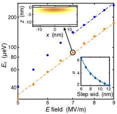
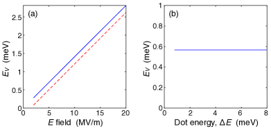
We now argue that the strong dependence of mobility gap on electric field can be understood as a consequence of steps at the quantum well interface. We perform tight binding calculations that include the vertical electric field and interfacial roughness, the latter in the form of uniformly spaced single-atomic steps (see supplementary material for details of the simulations). Fig. 4(a) shows the valley splitting as a function of the vertical electric field for step separations of 9.4 nm. This value was chosen so that the range of valley splittings, from 30 to 200 eV, matches the experimental measurements reported in Fig. 3. The power law dependence of the calculated valley splitting on electric field is found to be , extremely close to the experimental result of 2.7. This correspondence is remarkable, as shown in the lower right inset, which plots as a function of step width, revealing that even a relatively small change in step width can easily change the power law scaling away from that shown in the main panel of Fig. 4. The large observed value of is also remarkable for deviating so strikingly from the expectation that =1 Ando et al. (1982); Friesen et al. (2007); Boykin et al. (2004); Yang et al. (2013); Gamble et al. (2016), which only occurs in the limit of very low disorder, as indicated by the asymptotic behavior of Fig. 4, lower inset, and supplementary material. The similarity of the exponent for the three samples is evidence that the step densities are essentially inherited from the relaxed buffer growth and underlying substrate, and do not depend on the details of the top interface or the alloy disorder occurring there. This step separation corresponds to a miscut angle (0.8∘), which is larger than the sample miscut angles (=0.1-0.2∘) measured with X-ray diffraction, a fact that is unsurprising, because the epitaxial growth process is expected to yield additional steps that go up and down away from the average slope. Such increases in roughness are well known in strained epitaxial growth Evans et al. (2012).
Extrapolating these quantum Hall results to quantum dots is not unreasonable, with the following important caveats. First, the energy gaps obtained by activation measurements in quantum Hall experiments are actually mobility gaps, which are affected by electron-electron interactions and localized impurities Prange and Girvin (1990). Our estimates for the -factor indicate differences between the measured mobility gap and the expected single-particle Zeeman splitting on the order of 10%. Second, the quantum Hall requirement that , for constant filling factor, does not apply to dots, where the confinement potential is typically defined by a fixed gate arrangement and the voltages applied to those gates. For example, a typical orbital energy of =0.5 meV in a quantum dot corresponds to an r.m.s. radius of 20 nm, while the magnetic confinement in the =3 Landau level at =5.5 T corresponds to an r.m.s. radius of 7.7 nm. Quantum Hall transport measurements are therefore exposed to fewer atomic steps at the quantum well interface, and should typically reveal valley splittings larger than in quantum dots, for the same electric field. Finally, it is important to note that transport measurements effectively average over mesoscopic length scales, while quantum dot measurements do not. However, our theoretical analysis of the parameter demonstrates that single-electron physics provides key insights into the observed behavior.
In summary, we conclude that it is possible to control composition in the growth direction on the very short length scales appropriate for engineering enhancements in the valley splitting Zhang et al. (2013). In principle, this could be a useful tool for eliminating valley splitting effects arising from alloy disorder in SiGe barriers; however the dominant effect on the valley splitting, for the samples considered here, appears to arise from interfacial steps and atomic-scale disorder in the heterostructure layers below the top quantum well interface. Better control of this disorder is therefore essential for increasing the valley splitting in Si/SiGe heterostructures in future experiments.
See supplementary material for details on the activation energy analysis and the tight-binding methods.
We acknowledge helpful discussions with H.-W. Jiang, R. Joynt, and C. A. Richter. This research was sponsored in part by the Army Research Office (ARO) under Grant Numbers W911NF-17-1-0274, W911NF-12-1-0607 and by NSF (DMR-1206915), and by the Vannevar Bush Faculty Fellowship program sponsored by the Basic Research Office of the Assistant Secretary of Defense for Research and Engineering and funded by the Office of Naval Research through Grant No. N00014-15-1-0029.. Development and maintenance of the growth facilities used for fabricating samples is supported by DOE (DE-FG02-03ER46028). The views and conclusions contained in this document are those of the authors and should not be interpreted as representing the official policies, either expressed or implied, of the Army Research Office (ARO), or the U.S. Government. The U.S. Government is authorized to reproduce and distribute reprints for Government purposes notwithstanding any copyright notation herein. We acknowledge the use of facilities supported by NSF through the UW-Madison MRSEC (DMR-1121288).
Supplementary Information
In these Supplementary Materials, we provide additional experimental details, and describe our theoretical models and methods.
SI Spin Excitations at the Landau Level
In Fig. S1 we present the results of a spin-state activation experiment performed at , which was mentioned in the main text. The fitting procedure is analogous to the procedure discussed in Fig. 2 of the main text. By fitting the measured activation energy to the expected Zeeman splitting, , we obtain the estimates , , and for the Landé -factors in samples A, B, and C, respectively. The results differ by up to 10% from the expected value of for a Si quantum well. These variations can be attributed in part to changes in the mobility gap caused by electron-electron interactions and localization effects Prange and Girvin (1990).
SII Tight-Binding Hamiltonian
In order to incorporate atomic-scale disorder into our calculations, we adopt a two-band tight-binding Hamiltonian in two dimensions, as described in Boykin et al. (2004); Saraiva et al. (2010), with nearest and next-nearest-neighbor hopping parameters in the crystallographic direction, given by
| (S1) |
where are the valley minima in Si, for a cubic unit cell of size nm, and is the longitudinal effective mass. In the direction, we have just one nearest-neighbor hopping parameter, given by
| (S2) |
where is the transverse effective mass. For the two-band model, the atomic sites are arranged on a two-dimensional square lattice with atomic spacing .
Confinement potentials describing the quantum well barrier and the magnetic and electric fields are introduced into the tight-binding Hamiltonian through the on-site terms. For Si0.71Ge0.29 quantum well barriers, we assume a barrier height of 160 meV, while for Ge barriers, we assume a barrier height of 700 meV, corresponding to the band Schäffler (1997). We also include atomic-scale disorder (i.e., steps) in the position of the quantum well barrier, as indicated in Fig. 4(c) of the main text. For these simulations, we assume identical, uniformly spaced steps, which are conformal for all the different layer boundaries, yielding interfaces that are tilted away from the crystallographic axis by angle
The potential energy for a uniform electric field is given by . As in the experiments, the electric field, , is oriented perpendicular to the growth surface. As discussed in the main text, we adopt the quantum Hall constraint , which requires simultaneous variation of and , to achieve a constant filling factor .
We incorporate magnetic fields into the simulations through the Landau gauge, with the following considerations. In the quantum Hall regime, the wave functions of current-carrying electrons are localized in one direction, but extended in the orthogonal direction, along contour lines of constant potential Prange and Girvin (1990). For a quantum well with interfacial step disorder, such equipotential lines approximately follow the contours of the step. To a good approximation, the magnetic confinement of an electron therefore occurs in the direction transverse to the steps, which we define here as , relative to the growth direction, . For this geometry, the wavefunction component along is a simple plane wave, and we will ignore it here for simplicity. The resulting magnetic confinement potential is given by
| (S3) |
where is the cyclotron frequency, and is the center of confinement for the parabolic potential. In principle, could also be taken as an free parameter in our simulations; however, the valley splitting is not found to depend strongly on , and we simply choose it to coincide with a step rise, for convenience. To complete the tight-binding description, the potential terms and are simply evaluated at the lattice sites.
SIII Additional Tight-Binding Calculations
In the main text, we report a superlinear dependence of the valley splitting on the carrier density , and thus the electric field , which we attribute to the presence of interfacial disorder. To justify these claims, we describe here simulation results obtained in two related model systems, in the absence of interfacial disorder. In Fig. S2(a), we show that the valley splitting depends linearly on for a fixed confinement potential. In Fig. S2(b), we show that the valley splitting is independent of the confinement potential for constant . As shown in Fig. 4 of the main text, the valley splitting depends on both and the confinement potential when interfacial steps are present.
References
- Zwanenburg et al. (2013) F. A. Zwanenburg, A. S. Dzurak, A. Morello, M. Y. Simmons, L. C. L. Hollenberg, G. Klimeck, S. Rogge, S. N. Coppersmith, and M. A. Eriksson, Rev. Mod. Phys., 85, 961 (2013).
- Ando et al. (1982) T. Ando, A. B. Fowler, and F. Stern, Rev. Mod. Phys., 54, 437 (1982).
- Schäffler (1997) F. Schäffler, Semicond. Sci. Tech., 12, 1515 (1997).
- Ando (1979) T. Ando, Phys. Rev. B, 19, 3089 (1979).
- Friesen et al. (2006) M. Friesen, M. A. Eriksson, and S. N. Coppersmith, Appl. Phys. Lett., 89, 202106 (2006).
- Friesen et al. (2007) M. Friesen, S. Chutia, C. Tahan, and S. N. Coppersmith, Phys. Rev. B, 75, 115318 (2007).
- Kharche et al. (2007) N. Kharche, M. Prada, T. B. Boykin, and G. Klimeck, Appl. Phys. Lett., 90, 092109 (2007).
- Veldhorst et al. (2015) M. Veldhorst, C. H. Yang, J. C. C. Hwang, W. Huang, J. P. Dehollain, J. T. Muhonen, S. Simmons, A. Laucht, F. E. Hudson, K. M. Itoh, A. Morello, and A. S. Dzurak, Nature, 526, 410 (2015).
- Yoneda et al. (2018) J. Yoneda, K. Takeda, T. Otsuka, T. Nakajima, M. R. Delbecq, G. Allison, T. Honda, T. Kodera, S. Oda, Y. Hoshi, N. Usami, K. M. Itoh, and S. Tarucha, Nat. Nano., 13, 102 (2018).
- Zajac et al. (2018) D. M. Zajac, A. J. Sigillito, M. Russ, F. Borjans, J. M. Taylor, G. Burkard, and J. R. Petta, Science, 359, 439 (2018).
- Watson et al. (2018) T. F. Watson, S. G. J. Philips, E. Kawakami, D. R. Ward, P. Scarlino, M. Veldhorst, D. E. Savage, M. G. Lagally, M. Friesen, S. N. Coppersmith, M. A. Eriksson, and L. M. K. Vandersypen, Nature, 555, 633 (2018).
- Petta et al. (2005) J. R. Petta, A. C. Johnson, J. M. Taylor, E. A. Laird, A. Yacoby, M. D. Lukin, C. M. Marcus, M. P. Hanson, and A. C. Gossard, Science, 309, 2180 (2005).
- Maune et al. (2012) B. M. Maune, M. G. Borselli, B. Huang, T. D. Ladd, P. W. Deelman, K. S. Holabird, A. A. Kiselev, I. Alvarado-Rodriguez, R. S. Ross, A. E. Schmitz, M. Sokolich, C. A. Watson, M. F. Gyure, and A. T. Hunter, Nature, 481, 344 (2012).
- Wu et al. (2014) X. Wu, D. R. Ward, J. R. Prance, D. Kim, J. K. Gamble, R. T. Mohr, Z. Shi, D. E. Savage, M. G. Lagally, M. Friesen, S. N. Coppersmith, and M. A. Eriksson, Proc. Nat. Acad. Sci., 111, 11938 (2014).
- Nichol et al. (2017) J. M. Nichol, L. A. Orona, S. P. Harvey, S. Fallahi, G. C. Gardner, M. J. Manfra, and A. Yacoby, npj Quantum Inf., 3, 1 (2017).
- Gaudreau et al. (2011) L. Gaudreau, G. Granger, A. Kam, G. C. Aers, S. A. Studenikin, P. Zawadzki, M. Pioro-Ladrière, Z. R. Wasilewski, and A. S. Sachrajda, Nat. Phys., 8, 54 (2011).
- Medford et al. (2013) J. Medford, J. Beil, J. M. Taylor, S. D. Bartlett, A. C. Doherty, E. I. Rashba, D. P. DiVincenzo, H. Lu, A. C. Gossard, and C. M. Marcus, Nat. Nano., 8, 654 (2013).
- Eng et al. (2015) K. Eng, T. D. Ladd, A. Smith, M. G. Borselli, A. A. Kiselev, B. H. Fong, K. S. Holabird, T. M. Hazard, B. Huang, P. W. Deelman, I. Milosavljevic, A. E. Schmitz, R. S. Ross, M. F. Gyure, and A. T. Hunter, Science Adv., 1, 1500214 (2015).
- Kim et al. (2014) D. Kim, Z. Shi, C. B. Simmons, D. R. Ward, J. R. Prance, T. S. Koh, J. K. Gamble, D. E. Savage, M. G. Lagally, M. Friesen, S. N. Coppersmith, and M. A. Eriksson, Nature, 511, 70 (2014).
- Kim et al. (2015) D. Kim, D. R. Ward, C. B. Simmons, D. E. Savage, M. G. Lagally, M. Friesen, S. N. Coppersmith, and M. A. Eriksson, npj Quantum Inf., 1, 15004 (2015).
- Schoenfield et al. (2017) J. S. Schoenfield, B. M. Freeman, and H. Jiang, Nat. Commun., 8, 64 (2017).
- Thorgrimsson et al. (2017) B. Thorgrimsson, D. Kim, Y.-C. Yang, L. W. Smith, C. B. Simmons, D. R. Ward, R. H. Foote, J. Corrigan, D. E. Savage, M. G. Lagally, M. Friesen, S. N. Coppersmith, and M. A. Eriksson, npj Quantum Inf., 3, 32 (2017).
- Yang et al. (2013) C. H. Yang, A. Rossi, R. Ruskov, N. S. Lai, F. A. Mohiyaddin, S. Lee, C. Tahan, G. Klimeck, A. Morello, and A. S. Dzurak, Nat. Commun., 4, 2069 (2013).
- Gamble et al. (2016) J. K. Gamble, P. Harvey-Collard, N. T. Jacobson, A. D. Baczewski, E. Nielsen, L. Maurer, I. Montaño, M. Rudolph, M. Carroll, C. Yang, A. Rossi, A. Dzurak, and R. P. Muller, Appl. Phys. Lett., 109, 253101 (2016).
- Pla et al. (2012) J. J. Pla, K. Y. Tan, J. P. Dehollain, W. H. Lim, J. J. L. Morton, D. N. Jamieson, A. S. Dzurak, and A. Morello, Nature, 489, 541 (2012).
- Harvey-Collard et al. (2017) P. Harvey-Collard, N. T. Jacobson, M. Rudolph, J. Dominguez, G. A. Ten Eyck, J. R. Wendt, T. Pluym, J. K. Gamble, M. P. Lilly, M. Pioro-Ladrière, and M. S. Carroll, Nat. Commun., 8, 1029 (2017).
- Broome et al. (2018) M. A. Broome, S. K. Gorman, M. G. House, S. J. Hile, J. G. Keizer, D. Keith, C. D. Hill, T. F. Watson, W. J. Baker, L. C. L. Hollenberg, and M. Y. Simmons, Nat. Commun., 9, 980 (2018).
- Weitz et al. (1996) P. Weitz, R. Haug, K. von Klitzing, and F. Schäffler, Surf. Sci., 361-362, 542 (1996).
- Koester et al. (1997) S. J. Koester, K. Ismail, and J. O. Chu, Semicond. Sci. Tech., 12, 384 (1997).
- Lai et al. (2006) K. Lai, T. M. Lu, W. Pan, D. C. Tsui, S. Lyon, J. Liu, Y. H. Xie, M. Mühlberger, and F. Schäffler, Phys Rev B, 73, 161301(R) (2006).
- Goswami et al. (2007) S. Goswami, K. A. Slinker, M. Friesen, L. M. McGuire, J. L. Truitt, C. Tahan, L. J. Klein, J. O. Chu, P. M. Mooney, D. W. van der Weide, R. Joynt, S. N. Coppersmith, and M. A. Eriksson, Nat. Phys., 3, 41 (2007).
- Shi et al. (2011) Z. Shi, C. B. Simmons, J. Prance, J. K. Gamble, M. Friesen, D. E. Savage, M. G. Lagally, S. N. Coppersmith, and M. A. Eriksson, Appl. Phys. Lett., 99, 233108 (2011).
- Shi et al. (2014) Z. Shi, C. B. Simmons, D. R. Ward, J. R. Prance, X. Wu, T. S. Koh, J. K. Gamble, D. E. Savage, M. G. Lagally, M. Friesen, S. N. Coppersmith, and M. A. Eriksson, Nat. Comm., 5, 3020 (2014).
- Mi et al. (2015) X. Mi, T. M. Hazard, C. Payette, K. Wang, D. M. Zajac, J. V. Cady, and J. R. Petta, Phys. Rev. B, 92, 035304 (2015).
- Boykin et al. (2004) T. B. Boykin, G. Klimeck, M. A. Eriksson, M. Friesen, S. N. Coppersmith, P. von Allmen, F. Oyafuso, and S. Lee, Appl. Phys. Lett., 84, 115 (2004).
- Zhang et al. (2013) L. Zhang, J.-W. Luo, A. Saraiva, B. Koiller, and A. Zunger, Nat. Commun., 4, 2396 (2013).
- Simmons et al. (2009) C. B. Simmons, M. Thalakulam, B. M. Rosemeyer, B. J. V. Bael, E. K. Sackmann, D. E. Savage, M. G. Lagally, R. Joynt, M. Friesen, S. N. Coppersmith, and M. A. Eriksson, Nano Lett., 9, 3234 (2009).
- Wang et al. (2013) K. Wang, C. Payette, Y. Dovzhenko, P. W. Deelman, and J. R. Petta, Phys. Rev. Lett., 111, 046801 (2013).
- Ebert et al. (1983) G. Ebert, K. von Klitzing, C. Probst, E. Schuberth, K. Ploog, and G. Weimann, Solid State Communications, 45, 625 (1983).
- Usher et al. (1990) A. Usher, R. J. Nicholas, J. J. Harris, and C. T. Foxon, Phys. Rev. B, 41, 1129 (1990).
- Prange and Girvin (1990) R. E. Prange and S. M. Girvin, eds., The Quantum Hall Effect, 2nd ed. (Springer-Verlag, 1990).
- Lee and von Allmen (2006) S. Lee and P. von Allmen, Phys Rev B, 74, 245302 (2006).
- Ohkawa and Uemura (1977) F. J. Ohkawa and Y. Uemura, J. Phys. Soc. Jpn., 43, 907 (1977).
- Evans et al. (2012) P. G. Evans, D. E. Savage, J. R. Prance, C. B. Simmons, M. G. Lagally, S. N. Coppersmith, M. A. Eriksson, and T. U. Schülli, Adv. Mater., 24, 5217 (2012), ISSN 1521-4095.
- Saraiva et al. (2010) A. L. Saraiva, B. Koiller, and M. Friesen, Phys. Rev. B, 82, 245314 (2010).