Probing the Ultimate Plasmon Confinement Limits with a Van der Waals heterostructure
The ability to confine light into tiny spatial dimensions is important for applications such as microscopy, sensing and nanoscale lasers. While plasmons offer an appealing avenue to confine light, Landau damping in metals imposes a trade-off between optical field confinement and losses. We show that a graphene-insulator-metal heterostructure can overcome that trade-off, and demonstrate plasmon confinement down to the ultimate limit of the lengthscale of one atom. This is achieved by far-field excitation of plasmon modes squeezed into an atomically thin hexagonal boron nitride dielectric h-BN spacer between graphene and metal rods. A theoretical model which takes into account the non-local optical response of both graphene and metal is used to describe the results. These ultra-confined plasmonic modes, addressed with far-field light excitation, enables a route to new regimes of ultra-strong light-matter interactions.
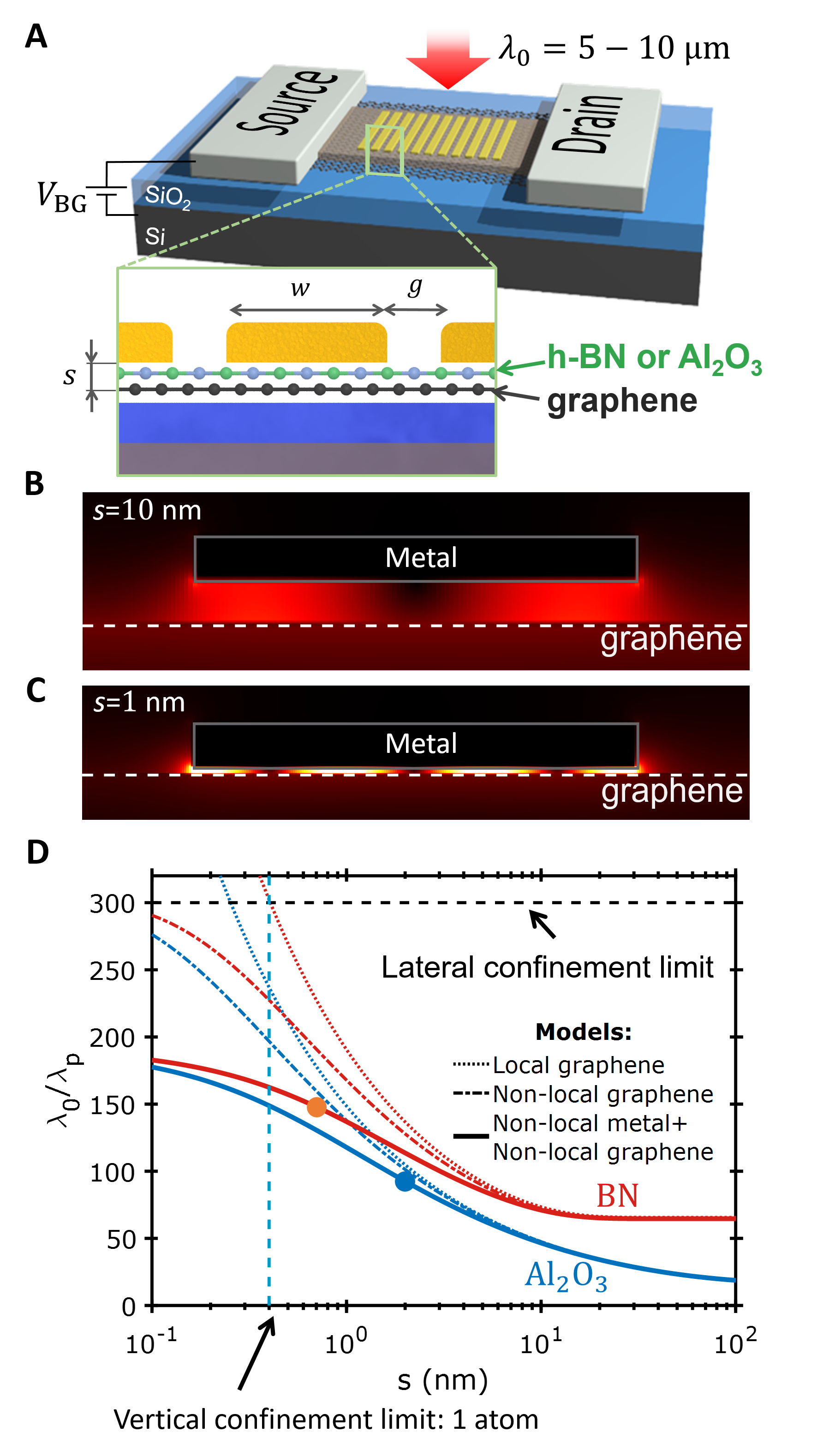
Van der Waals heterostructrures are constructed by vertically stacking atomically thin materials, selected from a rich palette of thousands of materials such as graphene (semi-metal), hexagonal boron nitride (h-BN, dielectric) and transition metal dichalcogenides (semi-conductors) (?). These are key enablers for tailoring electronic, optical and opto-electronic properties (?). The most common heterostructure for 2D electronics is graphene encapsulated by h-BN, and recently this system has also emerged as a platform for polaritonics (?, ?), with the capability to strongly confine plasmon polaritons with a relatively long plasmon lifetime exceeding 500 fs at room temperature (?). Heterostructures of graphene, h-BN, and metals have revealed so-called propagating acoustic plasmons (?, ?, ?), in which metal screening confines the light in the space between the metal and the graphene, and it slows down the plasmon to a velocity almost as low as /300 (with the speed of light) (?). What is then the ultimate limit on the confinement of propagating or resonant plasmons? For bulk metal-based plasmonic systems, such as tapers (?), grooves (?), metal-insulator-semiconductor (?), metal-insulator-metal (?, ?) waveguides, the confinement of propagating surface plasmon polaritons is limited by Landau damping (?). For example, the quality factor of plasmonic Fabry-Pérot modes dropped below one for a confinement below 15 nm (?). Further enhancement of optical fields to the nanometer scale is possible in hotspots (?, ?, ?), although these are broadband in character.
We present a graphene-insulator-metal platform that allows us to realize and probe the ultimate physical limits of (out-of-plane) confinement of propagating plasmons down to the ultimate physical boundary of one atom-thick layer (here ), and without sacrificing damping. We take advantage of the fact that plasmons in two-dimensional materials are fundamentally different from plasmons in bulk metals as the restoring force by the long-range Coulomb interactions, essential for the plasmon confinement, can be controlled by tailoring the external environment. For that reason the out-of-plane confinement and wavelength compression can be increased strongly without suffering from Landau damping. We use far-field light to couple to these strongly confined plasmons and find a vertical mode length down to 0.3 nm, while higher order Fabry-Pérot resonances reveal that the propagating character of the plasmons is preserved.
The basic device geometry consists of graphene as the plasmonic material, encapsulated by atomically thin dielectric materials (h-BN or \ceAl2O3) and covered by a metallic rod array (Fig. 1A) (see (?) for details on the fabrication processes). The advantages of the periodic metal-insulator-graphene system is twofold. First, the presence of the metal results in efficient screening of the graphene plasmons, squeezing the so-called screened graphene plasmons (SGPs) into the graphene-metal gap without reducing their lifetime. Although screening and coupling of radiation to plasmons in classical 2D electron gases (2DEG) was previously achieved using grating-gate field-effect-transistors in the THz range (?), a relatively thick barrier layer (nm) prevented the confinement of plasmons to the sub-nanometer limit, as we report here. Second, metal rods facilitate efficient coupling between far-field light and the strongly confined plasmons, where the width of the rods define the resonant conditions for the plasmon modes. This approach does not require patterning of the graphene into nanoribbons or nanodiscs as for previous infrared graphene plasmonic studies with far-field light (?, ?).
The effect of the coupling of far-field light into our devices is represented by the field profiles obtained by Finite-Difference-Time-Domain (FDTD) simulations (Figs. 1B, C). The plasmons are launched at the metal edges and most of the electric field is confined between metal and graphene, with virtually no leakage into the metal. This confinement arises because the metal acts as a nearly perfect conductor that prevents (most of the) field penetration. As image charges are induced in the metal, the plasmon mode is analogous to the anti-symmetric plasmon mode of two nearby graphene sheets with twice the spacer thickness (?), known as acoustic plasmons, carrying larger momentum than for conventional plasmon resonances in graphene ribbons (see (?), section 5.7). Within the dielectric gap, the plasmons maintain their propagating character and reflect at the edges of the rod, forming what appears to be a standing wave pattern similar to two coupled Fabry-Pérot resonators (?).
Bringing the metal closer will increase the plasmon screening, which slows down the plasmons as previously observed with s-SNOM by a proximity to a metal layer (?, ?), and also enhances the vertical confinement, as shown for two different materials and graphene conductivity models (local and non-local) (Fig. 1D). The most extreme case is that of a monolayer h-BN spacer, where in theory the vertical plasmon confinement is below 1 nm. Interestingly, the calculated width of the resonance (shown in (?), section 6) does not increase when reducing the spacer thickness . Therefore, this platform allows us to access the ultimate confinement limits of propagating plasmons in two spatial directions: out-of-plane confinement defined by and in-plane confinement governed by .
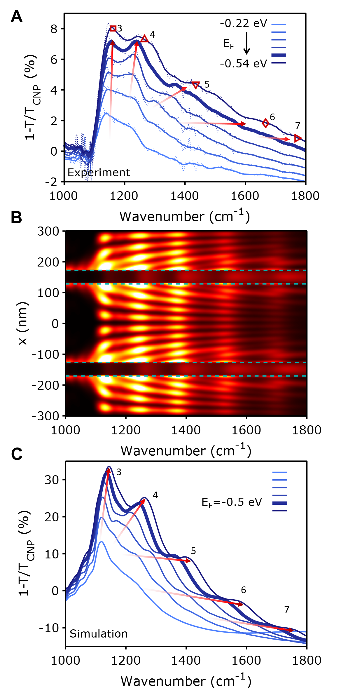
The far-field approach presented above allows probing of this plasmon confinement using Fourier Transform Infrared (FTIR) transmission measurements. Gate dependent, spectral extinction () curves are measured (Fig. 2A) for a device with continuous graphene (unpatterned), covered with nm \ceAl2O3 spacer ( nm) and metallic rods of 256 nm ( nm). These curves are obtained from the transmission curves normalized by the transmission of undoped graphene (at the charge neutrality point, CNP) for several gate voltages (hence, Fermi energies , see (?) section 2.2) at the same position, with light polarized perpendicular to the rods long axis. The spectra in Fig. 2a exhibit multiple resonances, which become more pronounced and continuously blue shift with increasing Fermi energies, thus confirming their plasmonic nature. The appearance of multiple peaks demonstrates that the incoming light can resonantly couple to higher orders of plasmonic modes than reported previously using nanoribbons (?). We find up to five visible resonances that can be controlled by the spacer thickness and the metallic array geometry.
We corroborate the phenomenon by examining the simulated electric field intensity profiles at the graphene surface for the same geometry as the measured device (Fig. 2B) and the corresponding simulated extinction spectra (Fig. 2C). The simulations, obtained by FTDT simulations (see (?) section 4), show a good agreement with the experiment (for =2nm) in terms of shape and peak position using the local optical response of graphene as well as a local metal permittivity models. The resonances can be related to Fabry-Pérot behavior of the propagating SGPs below the metal and the resonance orders can be approximated by the half number of nodes in the field profile (Fig. 2B). This observation confirms that resonances up to the order are contributing to optical extinction, while for patterned graphene (?, ?) only very weak second order resonances have been experimentally reported. We attribute the efficient launching of these higher-order resonances to the strong dipole modes at the metal edges ( (?) section 9), which provide the required momentum to scatter light into graphene plasmons.
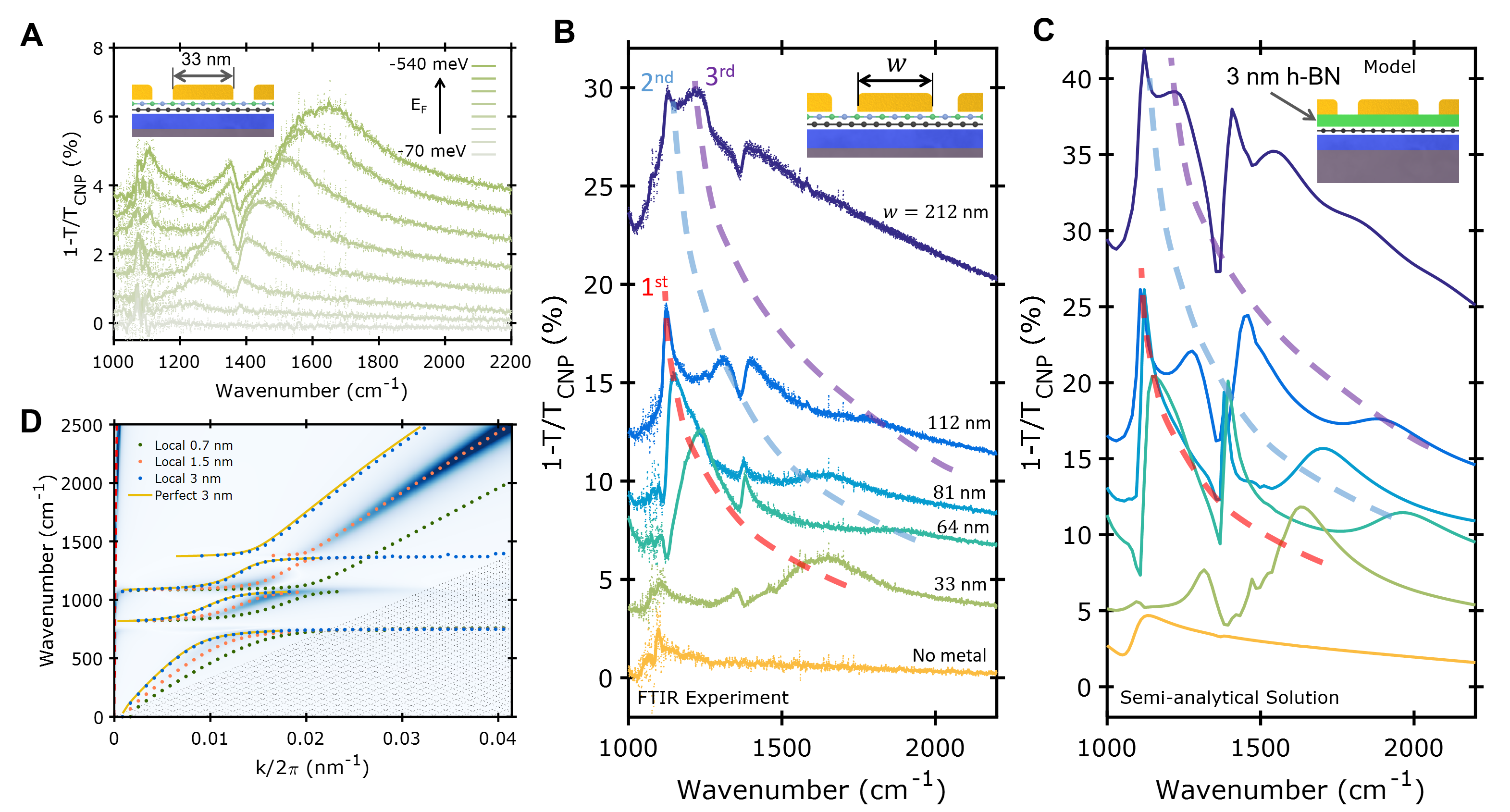
To probe the physical limits of SGP confinement we studied devices with a metal-graphene spacer with only one monolayer of CVD-grown h-BN of thickness 0.7nm (?, ?). The extinction spectra were obtained for various of a device with nm and nm (Fig. 3A). Strikingly, even in this case, the SGP resonances are still visible with high extinction values. A single plasmon peak is clearly visible and blue shifts for increasing , while hybridizing and anti-crossing with \ceSiO2 and \ceh-BN phonons. This shift with Fermi energy confirms that the extinction resonance is due to graphene plasmons.
The propagating character of the SGP modes can be assessed by further increasing , which allows us to probe higher order Fabry-Pérot resonances. We will show that this measurement is equivalent to changing the plasmonic cavity width which defines the resonant conditions. Extinction of several devices with increasing and similar gap around nm and doping of eV were studied (Fig. 3B). Additional doping dependences of these devices can be found in Fig.S5. The first order resonance (indicated by the red dashed lines in Fig 3B) displays hybridization with the optical phonons of its dielectric environment (as observed for plasmons in graphene nanoribbons (?)). We observe that when increasing , the first order resonance shifts to lower energies and hybridizes not only with the h-BN phonons, but also with the \ceSiO2 phonons. More resonances appear with increasing . For example, for , a second order resonance appears at 1900 cm-1 (green dashed line), which also shifts for larger and starts hybridizing when increasing . For the largest , the (pink dashed line) and even order resonances appear for our measurement range.
The same trends are seen in the calculated spectra (Fig. 3C), obtained from a semi-analytical approach, which consists of a Fourier decomposition of the fields (for TM-modes) in each dielectric region of the system (see (?) section 5). In addition, for these very tightly confined optical fields one must also take into account that the non-local optical response of both the metal and graphene can have appreciable effects. First of all, the in-plane momentum of the graphene plasmon is strongly enhanced by the presence of the metal and approaches , where the momentum dependence of the graphene optical conductivity (i.e. non-local corrections to the conductivity) increases (?). These graphene non-local corrections are modelled within the framework of the random-phase-approximation (RPA, see (?) section 5.6). Second, due to additional strong vertical field confinement of the order of 1 nm, the components of out-of-plane wavevectors approach , which is the Fermi momentum of the charge carriers in the metal (?). This trend can lead to additional non-local effects in the metal resulting in field penetration into the metal. It is therefore relevant to quantify these effects in order to determine fundamental limits of the vertical field confinement of the propagating plasmon.
Before we discuss a more rigorous treatment of the metal non-local effects, we provide a qualitative picture (?), where the non-local metal permittivity (NMP) was modelled as a dielectric shell surrounding a local metal permittivity (LMP) bulk material. Applying this model to our system we used a perfect conductor model (i.e. with zero damping) for the the bulk metal and the thickness of a uniform dielectric spacer is used as a fitting parameter. Simulations for this case, with an effective dielectric thickness of 3 nm (Fig 3C), show good agreement with the experiment (Fig 3B). Even though this result conflicts with the estimated spacer thickness ( nm), the non-local effect can be understood by the fact that the electromagnetic field does penetrate more into the metal for smaller (see Figs. 4 and S13) increasing the effective .
The excited plasmon modes associated with the extinction peaks in Figs 2 and 3 can be seen as a combination of SGPs under the metal and unscreened graphene plasmons in the gap region with their relative contribution depending on the geometry. Nevertheless, the calculated field profiles in Fig. 1b,c and the scaling of the plasmon resonance peak energy with clearly show that the electric field (associated with the plasmon modes) is mostly confined between the metal and the graphene. This confinement is also consistent with the observation that the plasmon resonances shift most significantly when varying compared to a change of the gap (see (?) section 3) and the fact that the system can be seen as a plasmonic crystal (analogous to photonic crystals) (?).
To further explore that a thicker dielectric in the LMP model results in non-local effects in the metal, the dispersion relation of the SGP modes is shown Fig 3D. The dispersion relation for a fully NMP model is offset to higher energies compared to a LMP model accounting for the proper h-BN thickness ( nm, green dotted line). Accounting for a thicker dielectric spacer used to fit our data ( nm), the dispersion curves shift down and overlaps with the NMP model. Qualitatively, this is in agreement with our findings. An additional shift is expected for a periodic structure instead of a continuous one as calculated in Fig 3D, because of a small coupling between the modes below the rods.
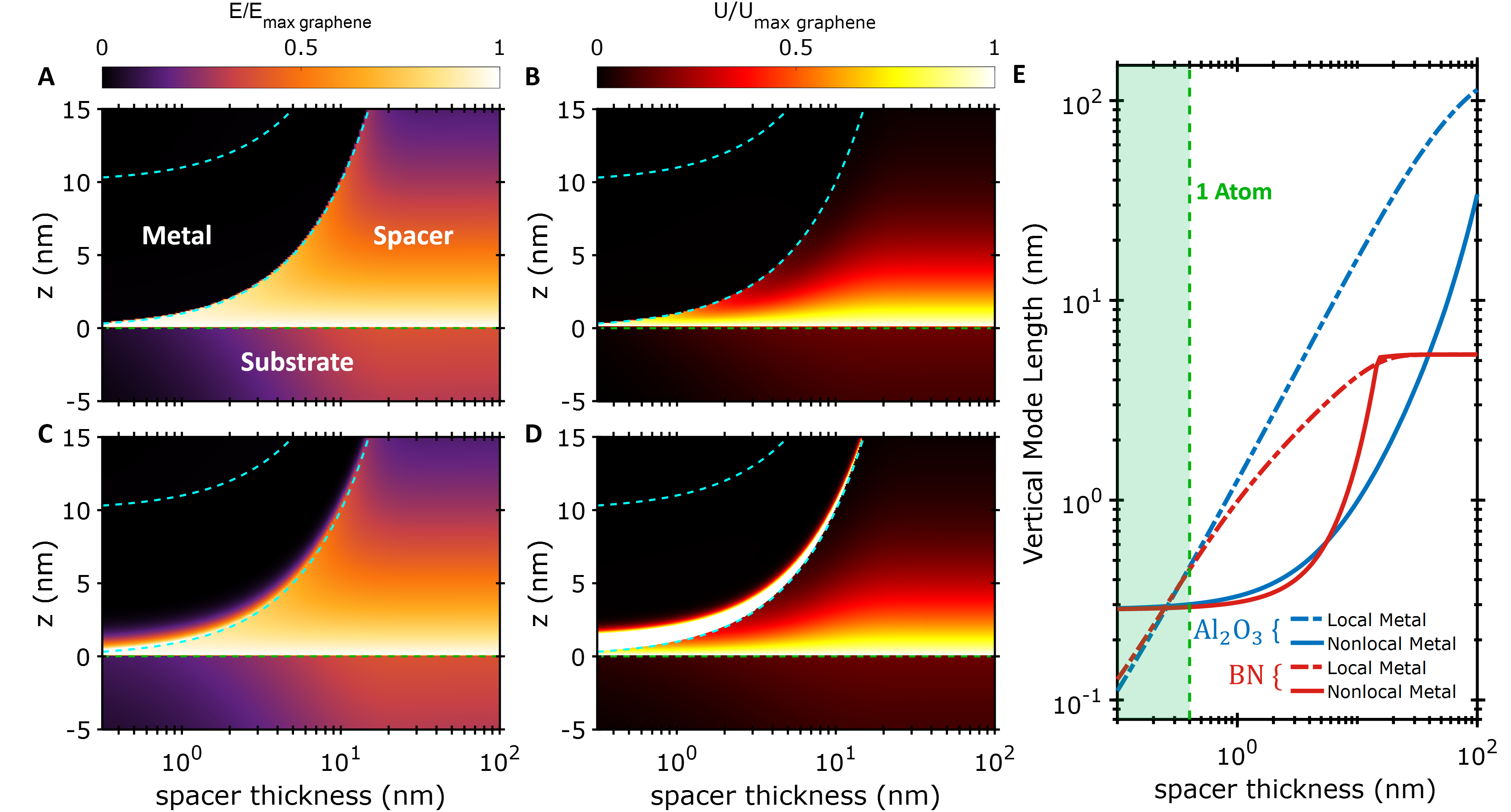
We can now evaluate the ultimate limit on the plasmonic vertical field and mode volume confinement. We have calculated the electric field intensity and energy density distribution for different spacer thicknesses (Fig. 4) and considered both LMP and NMP models. We used the definitions in section 5 of (?), taking into account dispersion effects. Inspecting first the electric field magnitude obtained from the LMP model and normalized by the maximum of the graphene plasmon (Fig. 4A,B), we find that most of it is confined between the graphene and the metal and the penetration of the field inside the the metal is negligible. On the other hand, considering metal non-local effects (NMP model) offers a more complete picture of the physics of the electrons that accumulate at the metal surface in order to screen the electromagnetic field (?). When the out of plane wavector is increased for thinner spacers, the electrons start suffering from Pauli and electrostatic repulsion. This effect results into a saturation of the electron density and leads to field penetration into the metal, as the metal screening capability is reduced (?). The penetration of the field into the metal becomes significant for below 3 nm, although the field remains maximum in the spacer region.
This non-local field penetration limits the vertical mode length, which is defined by the ratio of the energy density integrated over the out-of-plane coordinate to the maximum of the field intensity in the region of the spacer (?, ?):
| (1) |
The energy density distribution (Fig. 4D) peaks at the metal surface for a NMP model as a consequence of charge accumulation and the combination of high field and permittivity values, which is in contrast to the LMP (Fig. 4C). Below a certain spacer thickness, the energy density at the metal surface becomes larger than the energy density in the dielectric region near graphene. At this point the transition of the maximum energy density from graphene to the metal dominates the vertical mode length (Fig. 4E). The out-of-plane confinement is calculated from Eq. (1) and the energy density distribution that is shown in Fig. 4E. While for LMP, the vertical mode length can be made arbitrarily small, the non-local metal behaviour limits the vertical mode length to about 0.3 nm. This corresponds to a plasmonic mode confinement down to the atomic scale, as confirmed by our experiments.
These results raise the question why the plasmonic mode for nm, which penetrates the metal (due to non-local response), does not lead to strong (over)damping by Landau damping? For metals, the strongest confinement normal to the surface is limited by direct excitation of electron-hole pairs (Landau damping), accounted for by the non-local response function (?). A quantitive analysis of the metallic non-local corrections to the dynamic response and damping (?, ?) trough the Feibelman parameters revealed that these effects are much stronger for approaching . Interestingly, for , the imaginary part of the Feibelman parameters approaches zero, as the phase space for electon-hole excitations decreases with . The real part of the Feibleman parameters do not approach zero for . Thus, for our experimental conditions, the metal non-local effects are relevant as the electrons in the metal cannot perfectly screen the field, but the additional damping from electronic excitations in the metal is weak.
In terms of ultimate mode volume limit, we remark that a reduction of vertical confinement reduces also the lateral propagating plasmon wavelength (Fig. 1D). While our experiment discloses the fundamental limits of the vertical mode length of , it also allows us to estimate the complete mode volume confinement with respect to the volume associated with the extent of the free photons . If instead of an array (as in this work) a single resonant structure (e.g. a metal disc on graphene, with a monolayer h-BN spacer) was built using our approach, a vertical mode length down to nm and plasmon wavelenth (see Fig. 1D) would be attainable. Using these values (for ) that include the full non-local response for both graphene and metal, this would correspond to a mode volume of and mode volume ratio , which is at least two orders of magnitude smaller than reported so far with graphene nanoribbons (?), and sufficiently high to explore new regimes of light-matter interactions such as the ultra-strong coupling regime.
Our results show that 2D-material heterostructures can be considered as a powerful toolbox for nano-photonics with vertical sub-nanometer precision. We use this to combine efficient coupling between radiation and plasmons with extreme confinement, and found that propagating graphene plasmons can be confined down to 0.3 nm and drive a low-loss non-local metal response. The metallic structure can also be used as a nearby efficient gate (?) which provides a route to low-voltage applications to study molecular sensing with even higher resolution, to enhance non-linear effects, or to design photodetectors with plasmon enhanced sensitivity and tunability.
References
- 1. A. K. Geim, I. V. Grigorieva, Nature 499, 419 (2013).
- 2. K. Novoselov, A. Mishchenko, A. Carvalho, A. C. Neto, Science 353 (2016).
- 3. T. Low, et al., Nature materials 16, 182 (2017).
- 4. D. Basov, M. Fogler, F. G. de Abajo, Science 354 (2016).
- 5. A. Woessner, et al., Nature Mater. 14, 421 (2015).
- 6. A. Principi, R. Asgari, M. Polini, Solid State Communications 151, 1627 (2011).
- 7. V. V. Popov, Journal of Infrared, Millimeter, and Terahertz Waves 32, 1178 (2011).
- 8. P. Alonso-González, et al., Nature nanotechnology 12, 31 (2017).
- 9. M. B. Lundeberg, et al., Science 357, 187 (2017).
- 10. M. I. Stockman, Physical Review Letters 93, 137404 (2004).
- 11. S. I. Bozhevolnyi, V. S. Volkov, E. Devaux, T. W. Ebbesen, Physical Review Letters 95, 046802 (2005).
- 12. R. F. Oulton, V. J. Sorger, D. A. Genov, D. F. P. Pile, X. Zhang, Nature Photonics 2, 496 (2008).
- 13. J. A. Dionne, L. A. Sweatlock, H. A. Atwater, A. Polman, Physical Review B 73, 035407 (2006).
- 14. H. T. Miyazaki, Y. Kurokawa, Physical review letters 96, 097401 (2006).
- 15. S. Bozhevolnyi, L. Martin-Moreno, F. Garcia-Vidal, Quantum Plasmonics, Springer Series in Solid-State Sciences (Springer International Publishing, 2016).
- 16. C. Ciraci, et al., Science 337, 1072 (2012).
- 17. F. Benz, et al., Science 354, 726 (2016).
- 18. T. V. Teperik, P. Nordlander, J. Aizpurua, A. G. Borisov, Physical review letters 110, 263901 (2013).
- 19. V. W. Brar, M. S. Jang, M. Sherrott, J. J. Lopez, H. A. Atwater, Nano Letters 13, 2541 (2013).
- 20. H. Yan, et al., Nature Photonics 7, 394 (2013).
- 21. See the supplementary materials.
- 22. I.-T. Lin, C. Fan, J.-M. Liu, IEEE Journal of Selected Topics in Quantum Electronics 23, 144 (2017).
- 23. Z. Fang, et al., ACS Nano 7, 2388 (2013).
- 24. K. K. Kim, et al., Nano Letters 12, 161 (2012).
- 25. J. H. Park, et al., ACS Nano 8, 8520 (2014).
- 26. V. W. Brar, et al., Nano Lett. 14, 3876 (2014).
- 27. Y. Luo, A. I. Fernandez-Dominguez, A. Wiener, S. A. Maier, J. B. Pendry, Physical Review Letters 111, 1 (2013).
- 28. C. David, F. J. G. de Abajo, ACS-Nano 8, 9558 (2014).
- 29. R. Ruppin, Physics letters A 299, 309 (2002).
- 30. S. A. Maier, Optics Express 14, 1957 (2006).
Acknowledgments
The authors thank Gerasimos Konstantatos and Valerio Pruneri for the intensive use of their respective FTIRs, very insightful discussions with Marco Polini, Thomas Christensen, Asger Mortenson and Javier Aizpurua on non-local effects and with Achim Woessner on simulation and modelling of graphene acoustic plasmons modes. Funding: We acknowledge financial support from the Spanish Ministry of Economy and Competitiveness, through the Severo Ochoa Programme for Centres of Excellence in R&D (SEV-2015-0522), support by Fundacio Cellex Barcelona, the Mineco grants Ramon y Cajal (RYC-2012-12281), Plan Nacional (FIS2013-47161-P and FIS2014-59639-JIN), and the Government of Catalonia trough the SGR grant (2014-SGR-1535). Furthermore, the research leading to these results has received funding from the European Union H2020 Programme under grant agreement no. 604391 Graphene Flagship, the ERC starting grant (307806, CarbonLight) and project GRASP (FP7-ICT-2013-613024-GRASP). D.A.I. acknowledges the FPI grant BES-2014-068504. N.M.R.P. and E.J.C.D acknowledge support from the Portuguese Foundation for Science and Technology (FCT) in the framework of the Strategic Financing UID/FIS/04650/2013. This work was supported in part by the Center for Excitonics, an Energy Frontier Research Center funded by the U.S. Department of Energy, Office of Science, Office of Basic Energy Sciences under Award No. DE-SC0001088, and the Army Research Office (grant number 16112776). J.-Y.H. and J.K. acknowledge support from the US AFOSR FATE MURI, Grant No. FA9550-15-1-0514. Author contributions: F.H.L.K, D.A.I. and S.N. conceived the idea; E.J.C.D and N.M.R.P. developed the analytical model; S.N., C.P., J.O., D.E. and D.A.I. fabricated the devices; S.N., R.P. and D.A.I. performed measurements; D.A.I., M.L., I.E., and S.N. performed data analysis; J.Y.H. and J.K. provided h-BN; D.A.I., S.N., E.J.C.D., N.M.R.P, I.E., D.E. and F.H.L.K wrote the manuscript; D.E. and F.K. supervised the project. Competing interests: None of the authors have competing interests. Data and materials availability: All data needed to evaluate the conclusions in the paper are present in the paper and/or the Supplementary Materials
Supplementary materials
Materials and Methods
Supplementary Text
Figs. S1 to S17
References (32-46)