Radiofrequency generation by coherently moving fluxons
Abstract
A lattice of Abrikosov vortices in type II superconductors is characterized by a periodic modulation of the magnetic induction perpendicular to the applied magnetic field. For a coherent vortex motion under the action of a transport current, the magnetic induction at a given point of the sample varies in time with a washboard frequency , where is the vortex velocity and is the distance between the vortices in the direction of motion. Here, by using a spectrum analyzer connected to a 50 nm-wide Au nanowire meander near the surface of a superconducting Nb film we detect an ac voltage induced by coherently moving fluxons. The voltage is peaked at the washboard frequency, , and its subharmonics, , determined by the antenna width. By sweeping the dc current value, we reveal that can be tuned from MHz to GHz, thereby demonstrating that patterned normal metal/superconductor nanostructures can be used as dc-tunable generators operating in the radiofrequency range.
Magnetic fields are known to penetrate type II superconductors in the form of Abrikosov vorticesAbrikosov (1957), or fluxons, each carrying one quantum of magnetic flux Vs. The vortices form a triangular lattice and can be regarded as tiny solenoids producing local magnetic field variations extending over distances of perpendicular to the applied field, where is the magnetic penetration depth. The maximum field, Brandt (1995), occurs in the vortex core with a diameter of , where is the superconducting coherence length. A transport current of density exerts a Lorentz force on the flux lattice. If exceeds the pinning force, the vortex lattice moves and the oscillations of the magnetic induction at a given point in space are characterized by the washboard frequency , where is the vortex velocity and is the distance between the vortices in the direction of motion.
Previously, the washboard frequency of the moving vortex lattice was detected by ac/dc interference Harris et al. (1995) in high-temperature superconducting cuprates. The detected sharp frequencies Harris et al. (1995) were intrinsic to the moving lattice whose uniform motion in a random distribution of pinning sites produced a periodic modulation of the pinning force. If the dc driving current is augmented by an rf component an interference between the intrinsic oscillations and the superimposed ac current occurs when both frequencies are harmonically related Fiory (1971). Quantum interference effects are seen as Shapiro steps in the current-voltage characteristics Shapiro (1963); Martinoli et al. (1975); Dobrovolskiy (2017) when one or a multiple of the hopping period of Abrikosov vortices in superconductors with periodic pinning coincides with the period of the ac drive. In a different physical context, voltage oscillations at the washboard frequency were observed as narrow band noise in the sliding state of charge-density wave conductors Fleming and Grimes (1979), as well as in sliding spin-wave states Barthel et al. (1993).
The different dynamic states and noise associated with the vortex motion in type II superconductors was studied in several numerical works Olson, Reichhardt, and Nori (1998a, b). In particular, they predicted the broad band noise near depinning, the time of flight signal and the washboard signal as well as the signal shift towards higher frequencies with increasing dc drive. Recently, a similar study was also done for skyrmion lattices Díaz et al. (2017). The spectral analysis of the skyrmion velocity noise fluctuations has revealed broad band, time of flight and narrow band noise signals as well.
As distinct from the previously mentioned “intrinsic” effects, according to Faraday’s law, a time-varying magnetic flux within a closed loop of wire produces an electromotive force (emf) or voltage (within a circuit). This makes it feasible to observe the rf signal associated with the vortex motion externally, by placing a device which is sensitive to the magnetic flux near the surface of a superconductor. Currently, the highest flux sensitivity is provided by SQUIDs Fagaly (2006) which allow one to detect signals produced by the spin magnetic moment of a single electron Vasyukov et al. (2013). SQUID-based devices are successfully used for the visualization of nanoscale inhomogeneous magnetic states Anahory et al. (2016) and the high-velocity dynamics of individual vortices Embon et al. (2017). In general, electromagnetic radiation from a moving vortex lattice is also expected as it comes to a sample surface Bulaevskii and Chudnovsky (2006). This electromagnetic radiation at and its harmonics up to the superconducting gap frequency is generated by oscillating electric and magnetic fields of vortices near the surface and propagates into free space due to the continuity of tangential components of the fields at the surface. The effect of an external high-frequency stimulus on the dynamics of Abrikosov vortices in superconducting thin films has also been investigated experimentally Lara et al. (2015); Dobrovolskiy, Huth, and Shklovskij (2015); Lara et al. (2017); Dobrovolskiy et al. (2017) and theoretically Pompeo and Silva (2008); Shklovskij and Dobrovolskiy (2011). In particular, experiments provided evidence for stimulation of superconductivity by microwaves due to the presence of vortices Lara et al. (2015) and for enhanced stability of thermally-induced vortex avalanches under a microwave field excitation Lara et al. (2017).
In the particular case of coherently moving fluxons their dynamics can also be studied using hybrid, superconducting/normal metal detector structures. Given that nanowires with sub-100 nm width can be fabricated by modern nanofabrication techniques, vortex velocities of the order of 100 m/s allow one to achieve ac voltage frequencies, associated with crossing of nanowires by vortices, on the order of 1 GHz. Here, we study the frequency-domain voltage response of an Au meander nanowire which picks up the magnetic induction of magnetic flux quanta in an adjacent superconducting Nb thin film. While the meander layout is similar to those widely used in superconducting nanowire single-photon detectors (SNSPDs) Rath et al. (2015), here we use a quintuple, normally conducting meander with an active area of m2. The planar layout of the generator, designed to operate in a perpendicular magnetic field of mT, allows for easy on-chip integration with other fluxonic devices, such as diodes Villegas et al. (2003), microwave filters Dobrovolskiy and Huth (2015) and transistors Vlasko-Vlasov et al. (2016).

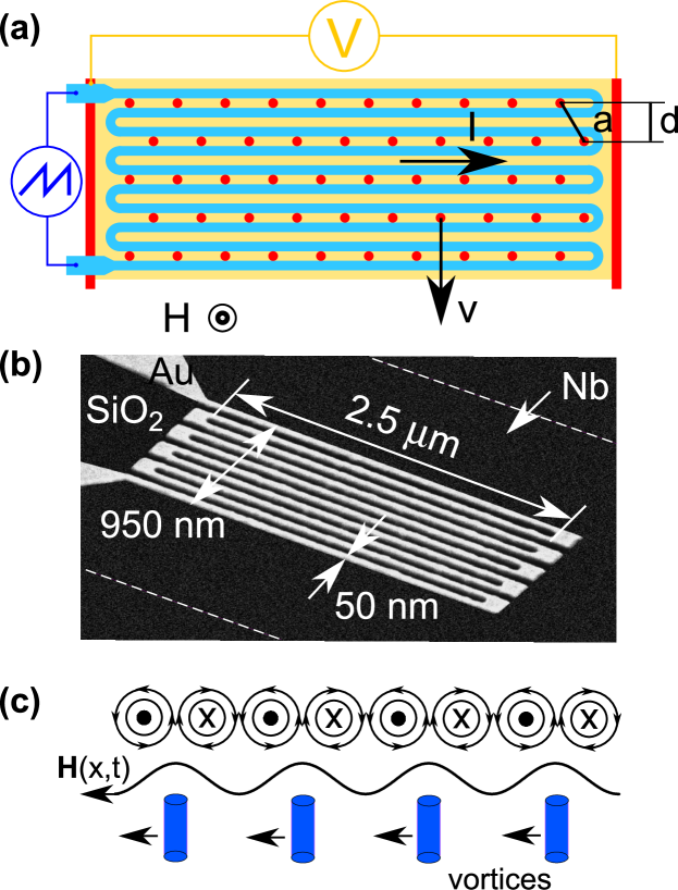
The device concept is sketched in Fig. 1(a). The device is based on a 45 nm-thick, 50 nm-wide Au meander nanowire connected to a high-frequency oscilloscope/spectrum analyzer (Tektronix MDO4024C) operating in the frequency domain. The nanowire was fabricated from an Au film by focused ion beam milling in a high-resolution scanning electron microscope (FEI Nova NanoLab 600). The Au film was prepared by dc magnetron sputtering onto Si/SiO2 substrate with a pre-sputtered 5 nm-thick Cr buffer layer. The thickness of the SiO2 layer was 200 nm. In the sputtering process the substrate temperature was C, the growth rate was nm/s and nm/s, and the Ar pressure was mbar and mbar for the Cr an Au layers, respectively. The nanowire consists of five periods (loops) to pickup the magnetic induction of moving vortices. A scanning electron microscopy image of the as-fabricated meander is shown in Fig. 1(b). The active area of the meander antenna was covered with a 10 nm-thick Al2O3 layer to avoid direct electrical contact with the superconductor which would otherwise shunt it. A four-point bridge was defined by UV-lithography in a 50 nm-thick Nb film with a width of m and a distance between the voltage contacts of m. The epitaxial (110) Nb film was sputtered by dc magnetron sputtering onto an a-cut sapphire substrate. In the sputtering process the film growth rate was nm/s, the substrate temperature was C, and the Ar pressure was mbar. The Nb film has a superconducting transition temperature of K and a room-to-10 K resistance ratio of 27. The upper critical field of the Nb film at zero temperature is mT as deduced from fitting the dependence to the phenomenological law . The values of the superconducting coherence length deduced from were found to be around nm. The estimated magnetic field penetration depth in the Nb film amounts to nm Gubin et al. (2005).
The Nb bridge was positioned by microscrews in the area encaged by the white dashed lines in Fig. 1(b). The in-plane angle alignment error with respect to the nanowire edges was less than . The Au meander was positioned in the geometrical center of the Nb bridge, to diminish the contribution of vortices pinned at the bridge edges. The measurements were done in a magnetic field mT directed perpendicular to the film surface. A dc transport current was applied through the Nb film parallel to the edges of the meander thus causing the vortices to move in the perpendicular direction, Fig. 1(a). The nanowire was connected via a -matched feed line to the port of the oscilloscope and we measured the rf voltage amplitude induced in the nanowire in terms of the spectral power density in the frequency range 50 MHz to 3 GHz.

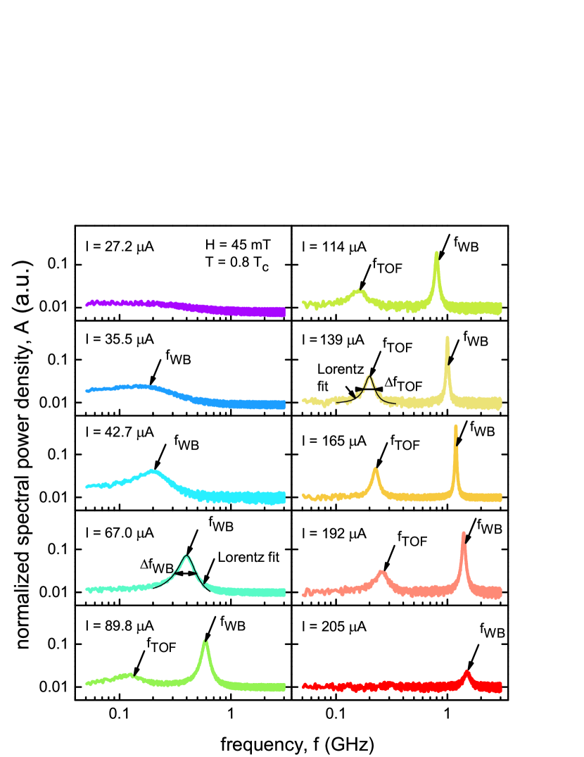
Figure 2 displays the frequency traces recorded by the spectrum analyzer for a series of dc currents flowing through the Nb film. At , there is no signal registered by the analyzer down to the noise floor at the -60 dBmV level. At small currents A the traces are flat, whereas at A a broad peak at MHz appears. With an increase of from A to A the magnitude of the peak increases and its frequency shifts to GHz. This is accompanied by the appearance of a second, broader and smaller peak on the low-frequency side of the large peak, which becomes visible at A at MHz. The maximal amplitude and the minimal linewidth of both peaks is observed at A at MHz and GHz, respectively. With a further increase of the current, the peaks become broader and their magnitudes decrease. The left peak vanishes at MHz at A while the right peak remains visible up to GHz at A.

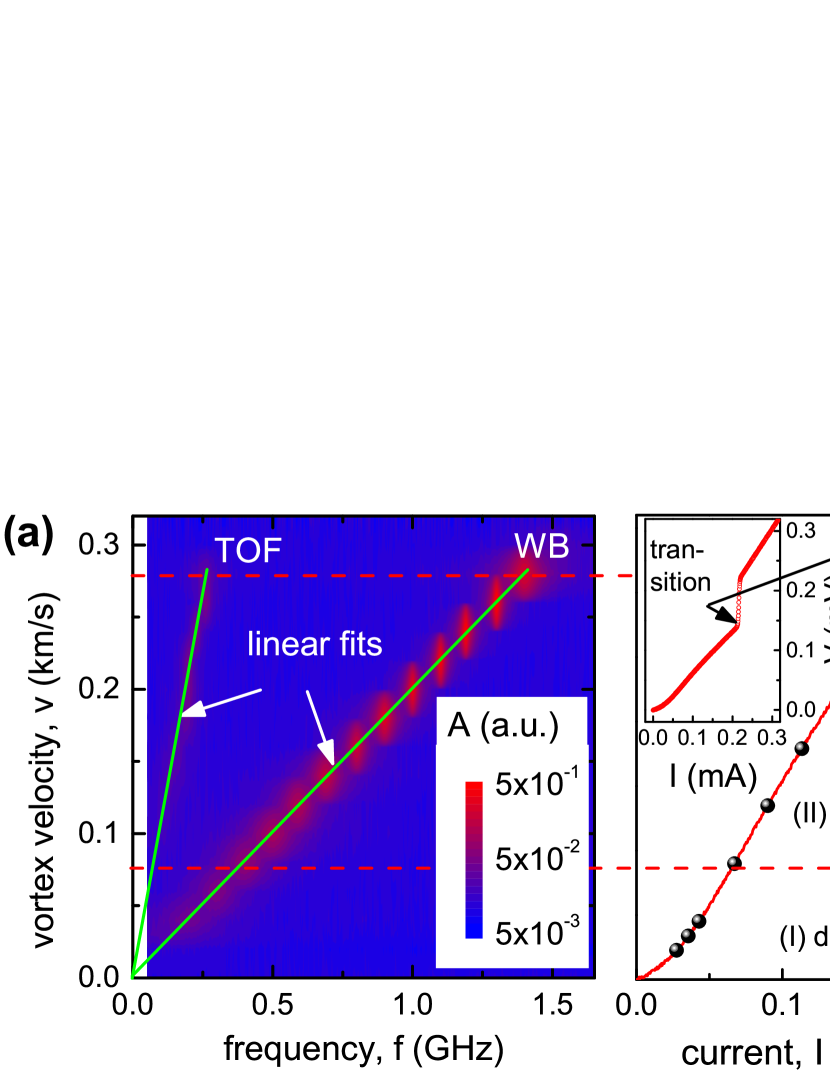
For a deeper analysis of the peaks associated with the vortex dynamics, in Fig. 3 we present the normalized spectral power density as a function of frequency and vortex velocity in comparison with the current-voltage-curve (CVC) of the Nb film. The vortex velocity was deduced from the CVC by the relation , where is the measured voltage, mT is the applied magnetic field, and m is the distance between the voltage contacts. In the contour plot in Fig. 3(a), two bright areas associated with the peaks in the spectra in Fig. 2 can be recognized. The broader and brighter one, which almost diagonally extends through the entire plot, corresponds to . The darker one, best seen between GHz and GHz at higher vortex velocities, relates to . The variation of color along the bright areas is associated with the coarse-grained vortex velocity points deduced from the CVC and included into the contour plot.
To elucidate what geometrical parameters of our system link the peak frequencies with the vortex velocities, we fit the bright areas in Fig. 3(a) to straight lines and , varying and as fitting parameters. The best fits are obtained with nm and m as shown in Fig. 3(a). corresponds very well to the meander period nm. is slightly larger than the distance between the outer edges of the meander nanowire nm. If we assume a triangular flux lattice with the parameter nm at mT and the matching condition , the arrangement of vortices in Fig. 1(a) allows us to explain both observed peaks as follows. At mT the triangular vortex lattice is commensurate with the meander nanowire and all vortices contribute to the produced voltage in phase. In this case the distribution of the magnetic induction is periodic in space and in time, where and are integers. The out-of-plane field components emanating from the vortices induce an Oersted field around the nanowire. As the vortices move, Fig. 1(c), the Oersted components oscillate in time and thereby produce an alternating ac voltage. Accordingly, the peak at occurs due to the vortices overcoming one period of the meander. The difference between and nm can be understood if we take into account two additional vortex rows at the outer edges of the meander, which contribute to the measured signal. If we add the radii of the vortices nm on each side of the meander to the meander width, the resulting m is in good agreement with . Therefore, the broader, low-frequency peak is related to the time needed for a vortex row to cross the meander from one outer edge to the other one. When the field is tuned in the range mT mT away from the matching condition, the peaks become broader but remain visible. At magnetic field values outside of this range no peaks are observed, which can be explained by the lost long-range order in the vortex lattice with respect to the meander. Therefore, we conclude that the coherence of the vortex dynamics is decisive for the observation of the rf generation by vortices.

The rf generation by vortices has been observed between and . At the amplitude of the detected signal decreased below the sensitivity level of our setup. This can be explained by the increase of the magnetic penetration depth at such that the modulation of the magnetic induction at the vortex cores and between them becomes very small. The particular set of data reported here was acquired at since at this temperature the depinning current is yet rather small and the peak frequency can be efficiently tuned by rather small currents. With nm and nm the magnetic induction variation at the vortex core and between the vortices can be estimated as mT, where nm, thus yielding Brandt (1995). According to Faraday’s law, a uniform -change of the magnetic flux for a single vortex moving with velocity m/s should produce an emf of V. Assuming that coherently moving vortices contribute to the emf additively, the emf produced by 50 vortices in our sample can be estimated as V. Obviously, this simple estimate is an upper-bound estimate as it does not account for signal losses due to the impedance mismatch between the nanowire and feed line.
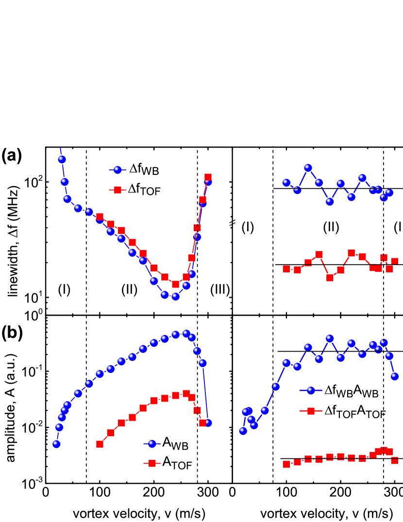
We now proceed to a quantitative analysis of the observed peaks. Both peaks can be fitted to the Lorentz distribution, which allows for a systematic analysis of their linewidth, , and magnitude, , as a function of the vortex velocity. The deduced dependences and are displayed in Fig. 4(a). The linewidth of both peaks exhibits a minimum at m/s with MHz. The amplitude of both peaks attains a maximum at the same velocity, Fig. 4(b). The ratio remains almost constant and equal to for vortex velocities between m/s and m/s, Fig. 4(c). The ratio is also almost constant in this range of vortex velocities. The fact that the magnitude of the peak at is an order of magnitude larger than that of the peak at can be explained by the five periods of the meander antenna acting in phase. If we introduce the products and as measures for the areas under the peaks, these will allow us to analyze the number of vortices contributing coherently to the measured rf voltage. Interestingly, at vortex velocities between m/s and m/s these products are almost constant, Fig. 4(d), suggesting that the number of vortices contributing to the signal is constant and we deal with a coherent vortex dynamics.
Outside of this range of vortex velocities, the area under the peak decreases, indicating that the number of vortices which takes part in the in-phase induction of voltage is decreasing as well. At small velocities this can be understood as a consequence of the depinning transition in the vortex dynamics. Indeed, even in high-quality films there is always a variation in the individual pinning forces acting on different vortices so that the long-range order in the vortex lattice is lost below the depinning transition. This corresponds to regime (I) in the CVC in Fig. 3(b). The spatial order of the vortex lattice in relation to the voltage noise spectra was studied numerically in Ref. Olson, Reichhardt, and Nori (1998a). It has been shown that the vortex velocity distribution function is most broad in the plastic phase near depinning and it is most narrow in the crystallinelike phase, just as we observe in our experiment. Namely, as soon as the viscous regime of flux flow is established, regime (II) in Fig. 3(b), the long-range order in the vortex lattice is recovered with increasing vortex velocity. This corresponds to a dynamic crystallization Koshelev and Vinokur (1994); Yaron et al. (1994) of the vortex lattice and this regime is stable as long as no further non-linearity comes into play. At high vortex velocities, regime (III), the electric field caused by the vortex motion accelerates quasiparticles in the vortex cores, which may escape from them. At the escape of quasiparticles leads to a shrinkage of the vortex core that, in return, causes a reduction of the vortex viscosity. The associated reduction of the viscous force impeding the vortex motion leads to a further increase of the vortex velocity resulting in a flux-flow instability Larkin and Ovchinnikov (1986); Bezuglyj and Shklovskij (1992); Shklovskij, Nazipova, and Dobrovolskiy (2017). This instability becomes apparent as a sudden transition of the sample into the normal state. In the inset to Fig. 3(b) we do not observe an abrupt jump, but rather a steep crossover from the flux-flow regime to the normally conducting state. This is because the flux-flow instability jump is expected to vanish above mT Larkin and Ovchinnikov (1986). Nevertheless, the linewidth broadening in Fig. 4(a) and the upturn in the CVC in Fig. 3(b) in regime (III) are indicative of the diminishing long-range order of the vortex lattice that can explain the vanishing peak at m/s.
To summarize, by using a spectrum analyzer connected to a nanowire meander near the surface of a superconducting Nb film we have detected an rf voltage induced by coherent vortex motion. The voltage is peaked at the washboard frequency and its subharmonics associated with the times needed for a vortex row to cross one meander period and the entire antenna, respectively. By sweeping the dc current value, we have been able to tune the generation frequency from MHz to GHz, thereby demonstrating that patterned hybrid nanostructures can be used as dc-tunable rf generators. The generation vanishes below the depinning transition, at high vortex velocities, and if the magnetic field value is tuned away from the matching configuration. Taken together, these findings underline the decisive role of the coherence in the vortex dynamics for the rf generation. Since the employed method relies on magnetic induction measurements rather than voltage, we anticipate that it can be applied to skyrmion systems as well Díaz et al. (2017).
OD acknowledges the German Research Foundation (DFG) for support through Grant No 374052683 (DO1511/3-1). This work was supported by the European Cooperation in Science and Technology via COST Action CA16218 (NANOCOHYBRI). Further, funding from the European Commission in the framework of the program Marie Sklodowska-Curie Actions — Research and Innovation Staff Exchange (MSCA-RISE) under Grant Agreement No. 644348 (MagIC) is acknowledged.
References
- Abrikosov (1957) A. A. Abrikosov, Sov. Phys. JETP. 5, 1174 (1957).
- Brandt (1995) E. H. Brandt, Rep. Progr. Phys. 58, 1465 (1995).
- Harris et al. (1995) J. M. Harris, N. P. Ong, R. Gagnon, and L. Taillefer, Phys. Rev. Lett. 74, 3684 (1995).
- Fiory (1971) A. T. Fiory, Phys. Rev. Lett. 27, 501 (1971).
- Shapiro (1963) S. Shapiro, Phys. Rev. Lett. 11, 80 (1963).
- Martinoli et al. (1975) P. Martinoli, O. Daldini, C. Leemann, and E. Stocker, Solid State Commun. 17, 205 (1975).
- Dobrovolskiy (2017) O. V. Dobrovolskiy, Physica C 533, 80 (2017).
- Fleming and Grimes (1979) R. M. Fleming and C. C. Grimes, Phys. Rev. Lett. 42, 1423 (1979).
- Barthel et al. (1993) E. Barthel, G. Kriza, G. Quirion, P. Wzietek, D. Jérome, J. B. Christensen, M. Jørgensen, and K. Bechgaard, Phys. Rev. Lett. 71, 2825 (1993).
- Olson, Reichhardt, and Nori (1998a) C. J. Olson, C. Reichhardt, and F. Nori, Phys. Rev. Lett. 81, 3757 (1998a).
- Olson, Reichhardt, and Nori (1998b) C. J. Olson, C. Reichhardt, and F. Nori, Phys. Rev. Lett. 80, 2197 (1998b).
- Díaz et al. (2017) S. A. Díaz, C. J. O. Reichhardt, D. P. Arovas, A. Saxena, and C. Reichhardt, Phys. Rev. B 96, 085106 (2017).
- Fagaly (2006) R. L. Fagaly, Rev. Sci. Instrum. 77, 101101 (2006).
- Vasyukov et al. (2013) D. Vasyukov, Y. Anahory, L. Embon, D. Halbertal, J. Cuppens, L. Neeman, A. Finkler, Y. Segev, Y. Myasoedov, M. L. Rappaport, M. E. Huber, and E. Zeldov, Nat Nano 8, 639 (2013).
- Anahory et al. (2016) Y. Anahory, L. Embon, C. J. Li, S. Banerjee, A. Meltzer, H. R. Naren, A. Yakovenko, J. Cuppens, Y. Myasoedov, M. L. Rappaport, M. E. Huber, K. Michaeli, T. Venkatesan, Ariando, and E. Zeldov, Nature Communications 7, 12566 EP (2016), article.
- Embon et al. (2017) L. Embon, Y. Anahory, Z. L. Jelic, E. O. Lachman, Y. Myasoedov, M. E. Huber, G. P. Mikitik, A. V. Silhanek, M. V. Milosevic, A. Gurevich, and E. Zeldov, Nat. Commun. 8, 85 (2017).
- Bulaevskii and Chudnovsky (2006) L. N. Bulaevskii and E. M. Chudnovsky, Phys. Rev. Lett. 97, 197002 (2006).
- Lara et al. (2015) A. Lara, F. G. Aliev, A. V. Silhanek, and V. V. Moshchalkov, Sci. Rep. 5, 9187 (2015).
- Dobrovolskiy, Huth, and Shklovskij (2015) O. V. Dobrovolskiy, M. Huth, and V. A. Shklovskij, Appl. Phys. Lett. 107, 162603 (2015).
- Lara et al. (2017) A. Lara, F. G. Aliev, V. V. Moshchalkov, and Y. M. Galperin, Phys. Rev. Appl. 8, 034027 (2017).
- Dobrovolskiy et al. (2017) O. V. Dobrovolskiy, M. Huth, V. Shklovskij, and R. V. Vovk, Sci. Rep. 7, 13740 (2017).
- Pompeo and Silva (2008) N. Pompeo and E. Silva, Phys. Rev. B 78, 094503 (2008).
- Shklovskij and Dobrovolskiy (2011) V. A. Shklovskij and O. V. Dobrovolskiy, Phys. Rev. B 84, 054515 (2011).
- Rath et al. (2015) P. Rath, O. Kahl, S. Ferrari, F. Sproll, G. Lewes-Malandrakis, D. Brink, K. Ilin, M. Siegel, C. Nebel, and W. Pernice, Light: Sci. Appl. 4, e338 EP (2015), original Article.
- Villegas et al. (2003) J. E. Villegas, S. Savel’ev, F. Nori, E. M. Gonzalez, J. V. Anguita, R. Garcia, and J. L. Vicent, Science 302, 1188 (2003).
- Dobrovolskiy and Huth (2015) O. V. Dobrovolskiy and M. Huth, Appl. Phys. Lett. 106, 142601 (2015).
- Vlasko-Vlasov et al. (2016) V. K. Vlasko-Vlasov, F. Colauto, T. Benseman, D. Rosenmann, and W.-K. Kwok, Sci. Rep. 6, 36847 EP (2016), article.
- Gubin et al. (2005) A. I. Gubin, K. S. Il’in, S. A. Vitusevich, M. Siegel, and N. Klein, Phys. Rev. B 72, 064503 (2005).
- Koshelev and Vinokur (1994) A. E. Koshelev and V. M. Vinokur, Phys. Rev. Lett. 73, 3580 (1994).
- Yaron et al. (1994) U. Yaron, P. L. Gammel, D. A. Huse, R. N. Kleiman, C. S. Oglesby, E. Bucher, B. Batlogg, D. J. Bishop, K. Mortensen, K. Clausen, C. A. Bolle, and F. De La Cruz, Phys. Rev. Lett. 73, 2748 (1994).
- Larkin and Ovchinnikov (1986) A. I. Larkin and Y. N. Ovchinnikov, “Nonequilibrium superconductivity,” (Elsevier, Amsterdam, 1986) p. 493.
- Bezuglyj and Shklovskij (1992) A. Bezuglyj and V. Shklovskij, Physica C 202, 234 (1992).
- Shklovskij, Nazipova, and Dobrovolskiy (2017) V. A. Shklovskij, A. P. Nazipova, and O. V. Dobrovolskiy, Phys. Rev. B 95, 184517 (2017).