Quantum wires and waveguides formed in graphene by strain
Abstract
Confinement of electrons in graphene to make devices has proven to be a challenging task. Electrostatic methods fail because of Klein tunneling, while etching into nanoribbons requires extreme control of edge terminations, and bottom-up approaches are limited in size to a few nm. Fortunately, its mechanical flexibility raises the possibility of using strain to alter graphene’s properties and create novel straintronic devices. Here, we report transport studies of nanowires created by linearly-shaped strained regions resulting from individual folds formed by layer transfer onto hexagonal boron nitride. Conductance measurements across the folds reveal Coulomb blockade signatures, indicating confined charges within these structures, which act as quantum dots. Along folds, we observe sharp features in traverse resistivity measurements, attributed to an amplification of the dot conductance modulations by a resistance bridge incorporating the device. Our data indicates ballistic transport up to 1 m along the folds. Calculations using the Dirac model including strain are consistent with measured bound state energies and predict the existence of valley-polarized currents. Our results show that graphene folds can act as straintronic quantum wires.
Keywords: Graphene, Straintronics, Synthetic gauge fields
Graphene, the one-atom-thick layer of carbon atoms arranged in a honeycomb structure, has remarkable electronic and mechanical properties1, 2. Electric fields3, 4, 5, spatial confinement6, 7, 8, 9, 10 and periodic potentials11, 12, 13, 14, 15 are just some of the methods used to manipulate its electronic behavior. As an atomically thin membrane, graphene is highly flexible16, 17 and strain engineering can also be used to control its electronic properties18, 19, 20, 21, 22, 23, 24. It was reported, for example, that in graphene nanobubbles strain-induced pseudomagnetic fields can reach magnitudes greater than 300 T19 while creating strong density of state modulations. Wrinkled or rippled graphene on SiO2 substrates25, 26, 27, 28 and suspended samples29 were also carefully studied, including investigation of electron-phonon scattering25, Kelvin probe microscopy of fold resistivity,28 potential fluctuations27, and the average impact on electrical resistance across many samples with large number of folds26. Furthermore, scanning tunneling microscopy measurements30 demonstrated that pseudomagnetic fields confine electrons in deformed regions locally creating quantum dots. Despite this progress, the use of strain to produce building blocks for electronic systems, such as quantum wires and coherent electron waveguides, although promising31 remains elusive, while even basic quantum transport properties are still unexplored.
In this work, we present transport measurements on graphene devices with well defined, isolated, linearly-shaped strained regions created by nanoscale-width folds. These folds are produced by placing graphene membranes onto hexagonal boron nitride (hBN) substrates32, which are supported by oxidized Si wafers. Attached source and drain electrodes enable measuring the differential conductance while tuning the charge density in the graphene using the Si wafer as a gate electrode. Charge transport is measured in perpendicular and parallel directions with respect to the fold axis orientation. Remarkably, measurements carried out with a perpendicular incident current exhibit single-electron charging and Coulomb blockade features, clear signs of charge confinement. Observed quantum level spacings and charging energies reveal the confinement to occur in regions of dimensions of the strained-fold width, indicating that the fold acts as a finite length one-dimensional (1D) quantum wire, likely broken into several shorter conducting segments by disorder. Experimental observations are in agreement with theoretical calculations that model the behavior in terms of a strain-induced pseudomagnetic field 18, 23 which creates barriers confining electrons to nanoscale channels. Transport with parallel incident current reveals sharp structures reminiscent of Fano-like features33, suggesting interference between conduction paths entirely within the graphene sheet, and states bound in the deformed region.
In addition to confining electrons to one dimension, the pseudomagnetic field is predicted to filter electrons from individual valleys23. We show the filtering depends on the incident angle of the incoming current, a unique feature that will enable the realization of valleytronic devices34, 35, 36, 23 by appropriate design of fold geometries. As the incidence angle can be controlled experimentally, a linearly strained graphene device such as the one reported in this work, can potentially serve as a valley filter for valleytronics applications.
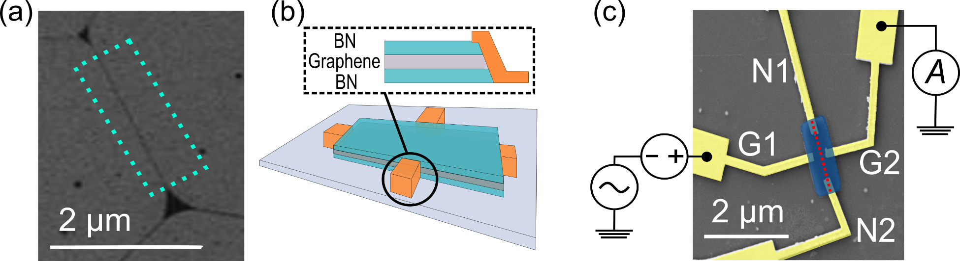
Figure 1a-c shows the typical device geometry. Devices are fabricated using Elvacite polymer layers and dry transfer to encapsulate graphene between hBN layers37. Figure 1a shows a Scanning Electron Microscope (SEM) image of a graphene flake with a linear strain (dark line) in the center after its dry-transfer to hBN. The cyan dashed outline encloses the graphene area later made into a device via etching. We distinguish two types of isolated folds (Supporting Information section 1)26. Type I is characterized by approximately Gaussian shapes with heights -measured by atomic force microscopy- between to nm, while Type II exhibits a flat-plateau geometry with reduced heights between to nm. It is likely that Type II folds result from Type I bent laterally to contact the graphene sheet26. Following fold identification, a top BN layer is added to encapsulate the graphene (Fig. 1b). Four electrical contacts are fabricated by an edge contact technique37 on the four sides of the BN/graphene/BN sandwich structure (Fig. 1b inset). A colorized SEM image of a device is shown in Fig. 1c, consisting of the encapsulated graphene (blue region) and electrical contacts (yellow regions) with a red dashed line indicating the location of the linear strain. Graphene sheet contacts are labeled G1 and G2, while nanowire contacts (as well as the top sides of the sheet) are labeled N1 and N2. The linear strain is located at the device center.
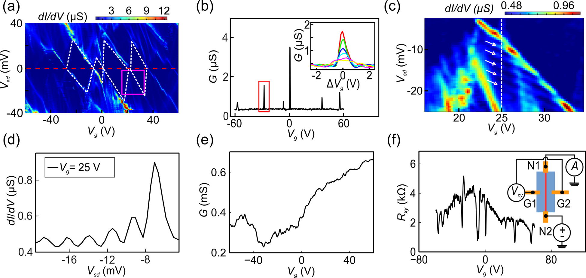
To study the electronic transport properties of the system, we first measure using the setup shown in Fig. 1c, with perpendicular current flow, i.e. between contacts G1 and G2, while floating contacts N1 and N2. The experiment is performed using a lock-in amplifier with a source-drain dc voltage () applied to G1 in addition to a small ac bias () voltage. The ac current () is measured vs. and gate voltage applied to the Si back gate. Figure 2a shows a color plot vs. and at K. Remarkably, the data show Coulomb diamond features similar to those previously observed in nanotubes38 or confined graphene39, a phenomena characteristic of charge confinement that occurs in quantum dot (QD) geometries. The bright lines (large values of ) represent the opening of seemingly quantized transport channels across the system. We estimate the charging energy for these regions from the voltage scale of the diamonds40 and obtain meV for the diamonds marked by the white dashed lines. Assuming the capacitance scales with the fold length (similar to carbon nanotubes) we obtain effective lengths of approximately nm. This suggests that disorder, lack of uniformity, or change of orientation (e.g., a kink) along the fold creates an effective shorter length (as compared with the distance N1-N2 m) that dominates the Coulomb blockade (CB) regime at zero bias.
Figure 2b shows a line trace at V (along the red dashed line in Fig. 2a). CB peaks are observed, separated by low conductance regions. These peaks occur when neighboring charge states become degenerate, enabling current flow by single-electron charging and discharging cycles. The low conductance regions, which appear as the dark blue diamond areas in Fig. 2a, correspond to a fixed charge state on the fold, and indicate that contacts N1 and N2 only make good electrical contact to the graphene on one side of the nanowire. The Fig. 2b inset shows the corresponding versus at different temperatures for the peak enclosed by the red rectangle in main panel. The curves shift slightly as the temperature changes, and is shifted accordingly to maintain the peak alignment. The amplitudes of the differential conductance peaks become smaller, and their widths become larger with increasing temperature. This indicates a resonant single quantum level transport process40. Coulomb oscillations persist up to the largest temperature measured of K, with little temperarure dependence in the conductance minima, as expected based on the measured charging energy meV.
A zoom-in image of data taken at finite bias from inside the magneta rectangle of Fig. 2a is shown in Fig. 2c. Parallel lines observed outside the insulating diamond-shaped regions correspond to tunneling through discrete energy excitations (marked as arrows in the figure).
Figure 2d shows a line trace of versus at V (along the white dashed line in Fig. 2c). Six peaks are evident in the figure. The left five peaks correspond to discrete energy excitations marked with arrows in Fig. 2c, while the right peak corresponds to reaching the condition where current flow is first enabled at the CB diamond boundary. Analysis of the data 40 reveals uniform energy level spacings of meV. Assuming a finite length 1D quantum wire geometry model without broken valley degeneracy (relaxing this assumption leads to similar results), the energy level spacing can be estimated by , where m/s is the Fermi velocity of the confined states and is an effective length m, a value larger than the scale estimated by the charging energy but similar in order of magnitude (see Supporting Information section 2). This indicates a ballistic mean free path along the nanowire up to m. Interpreting the data as arising from transport through dots of different sizes as suggested by the inferred lengths and and the several downward slopes in Fig. 2c, (see e.g. Abulizi et al. 41) is therefore consistent with a distorted or disordered fold extended along the sample between contacts N1 and N2.
We now turn to measurements with parallel incident current. Fig. 2e shows the conductance versus that is finite for the voltage range explored with no Coulomb peaks observed for this flow direction. This is consistent with the large resistance ratio between the quantum wire and flat sheet regions so that the bulk of the current flows through the flat regions. The fold is detected however, by its effects on the transverse resistance versus (where is the current in the direction parallel to the fold). The measurement setup is shown in the right inset of Fig. 2f, with current passed through contacts N1 and N2 and voltage measured across G1 and G2. Transverse resistance data taken at K shows small oscillations superimposed on large jumps that can be attributed to contributions from the confined states in the fold region and extended states in the graphene layer. The increased sensitivity of the transverse measurement to the presence of the finite size wire can be explained by the graphene sheets and voltage probes forming a Wheatstone bridge geometry with the nanowire dot acting as the bridge resistance (see Supplemental Information section 3). The sharp adjacent dip and peak in the data around is reminiscent of Fano interference processes42, which may occur between states in graphene and those dwelling temporarily on the nanowire, however more work will be required to fully elucidate the transport mechanism leading to this phenomenon.
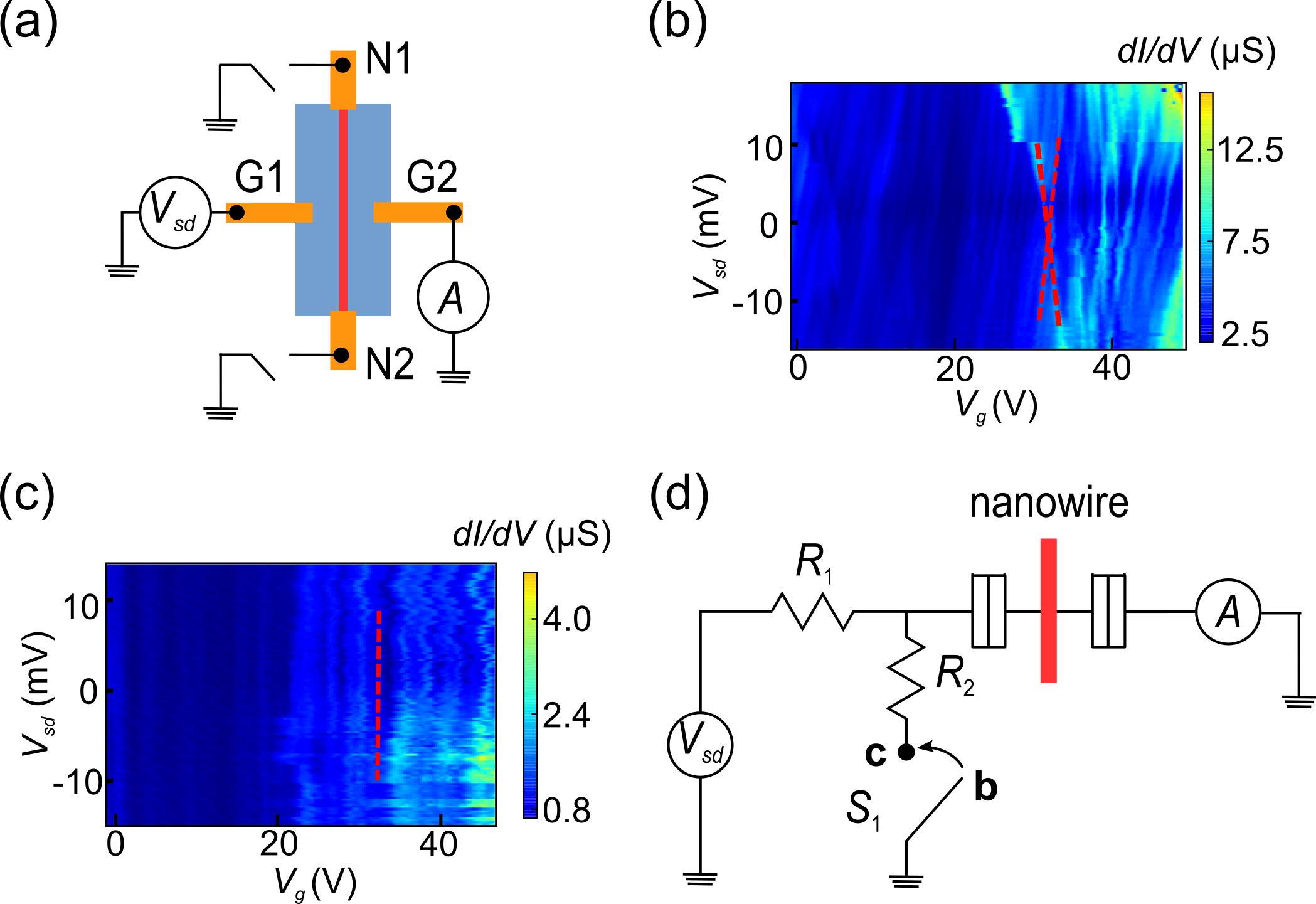
To further explore the nature of the confinement, we measured several different samples within the same device setup as Fig. 1c. The tunnel barriers between the linearly strained regions and the flat graphene layer and/or contacts N1 and N2 were found to vary between highly reflecting (yielding CB diamonds), and highly transmitting [yielding Fabry-Perot resonances 43]. The measurement setup is schematically shown in Fig. 3a. As before, data is obtained with the differential conductance taken across the linear strain with floating contacts N1 and N2 corresponding to open switches in Fig. 3a. Fig. 3b shows data taken for one Fabry-Perot type device, where neighboring diagonal linear features (dashed lines) appear with similar slopes over the entire gate voltage range explored. These features arise when the electrochemical potentials of the source and drain electrodes align with Fabry-Perot resonances in the finite size wire. For comparison, a set of data taken across the linear strain with electrodes N1 and N2 grounded is shown in Fig. 3c (Fig. 3a with closed switches), as a color plot for as a function of and . The criss-cross pattern associated with the Fabry-Perot interference disappears. Instead, discrete vertical linear features (dashed line) in the spectra can be identified.
This behavior can be accounted for by the schematic equivalent circuit diagram shown in Fig. 3d. In this setup, the nanowire appears as a high-impedance tunnel barrier, along with resistors and , and the switch . represents the flat graphene resistance connected to the nanowire on one side, while corresponds to the resistance to ground on the same side of the nanowire on the sheet. (A similar resistor network could be shown for the other side of the device, but is omitted for simplicity.) When N1 and N2 are floating, the switch in Fig. 3d is open (contact position b), only a negligible voltage drop occurs across and essentially the full source-drain voltage appears across the nanowire. On the other hand, when N1 and N2 are grounded, the switch is closed, (contact position c), the voltage is divided by the voltage division circuit formed by and . The vertical slope of the features shows that the electrons crossing the device through the nanowire have an energy near the electrochemical potential of the ground electrode, indicating that , consistent with the region of the charge confinement occurring near the nanowire. Based on this, we expect that the criss-cross pattern would be visible at larger voltages, scaled by , however to avoid potential electronic damage to the device, such larger voltages were not applied.
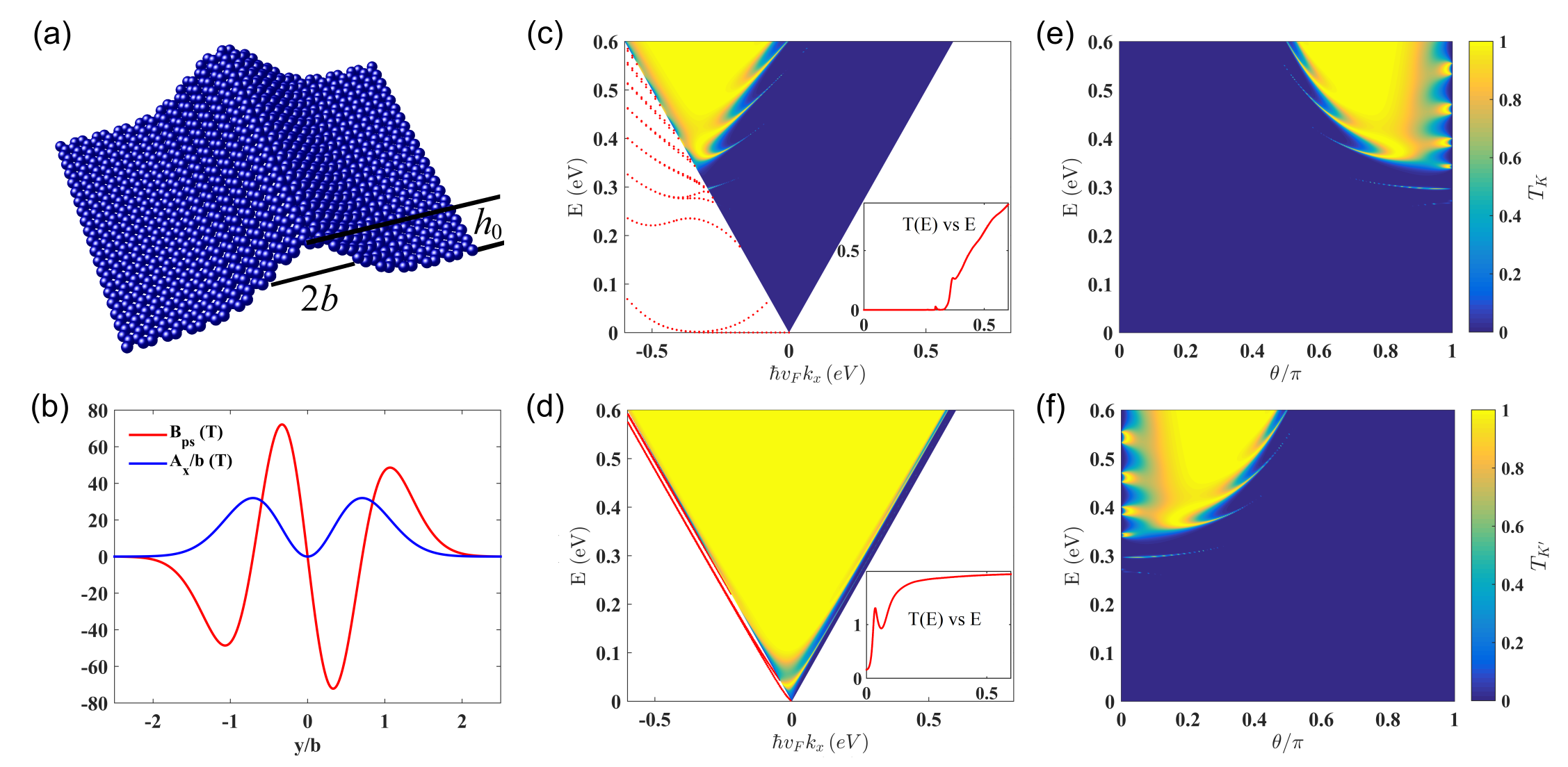
Taken together, the observed quantum levels and Fabry-Perot resonances show that the folds act as quantum wires and waveguides. While the structure of the folds is unknown after the capping BN layer is added, we confirmed that the initial folds are necessary to observe the electron confinement behavior. The stress associated with being placed between two layers with van der Waals adhesion forces could distort the initial fold shape, for example changing a type I structure to a type II, and Coulomb oscillations persist enhancing the strain and maximum curvature of the folds (see Supplemental Information, section 4). To gain insight into the origin of these features, we consider a model with a strained out-of-plane deformation depicted in Fig. 4a, which should be appropriate for modeling any sharp crease in graphene. We consider the in-plane displacement (expected from the mismatch with the hBN lattice) to be negligible as compared to the out of plane displacement. Due to the strong in-plane boding of carbons it is expected that the strain does not produce lattice defects44. Nevertheless, it is well established that strain strongly modifies the local density of states, giving rise to localized states in deformed regions18, 21, 20, 19, 30, 22. At low energies, the electron dynamics are described via a massless Dirac equation, with strain producing an effective pseudo-vector potential. In the valley isotropic basis , ( denote the two-atom basis), the Hamiltonian is18, 21, 20, 23: . Here, labels the two valleys, is the Pauli matrix vector, and the momentum. The strain tensor components , where and are in-plane and out-of-plane displacements, respectively and determine the pseudo-vector potential:
| (1) |
where Å, , predicted within a range of variation45, and () is along the zigzag (armchair) direction21. A Gaussian-shaped fold is represented by , with height and width as shown in Fig. 4a. The corresponding pseudo-vector potential is
| (2) |
where eV, , and . Fig. 4b shows the inhomogeneous amplitude of the pseudo-vector potential (blue) and its corresponding pseudomagnetic field (red).
Scattered and bound states are obtained with scattering matrix methods applied to incident states with energy and wave vector related by: , , where is measured with respect to the zigzag crystalline direction. Inside the folded region and . Thus, for appropriate values of and , can become imaginary and render zero transmission.
Fig. 4c shows the transmission spectra through a fold along the zigzag direction for valley (results for are mirror symmetric and not shown). Inside the original Dirac cone, the bright colored region represents non-zero transmission scattering states that fades as and becomes zero for imaginary (blue region). At low energies (E eV), transmission is almost forbidden for all incident angles, indicating a highly reflecting fold (see Fig. 4c inset). For (), sets of split resonances are visible. These states connect to the red dotted lines that represent the dispersion of bound states that propagate along the fold.
The orientation of the fold with respect to the crystalline axis strongly affects the strength of the pseudomagnetic field, and hence the system transport properties. For a fold along an arbitrary angle with respect to the zigzag direction, ( along the fold axis), making a fold with axis close to armchair directions highly transmitting. Fig. 4d shows transmission and bound state energies for a fold with axis away from the armchair direction. Strong transmission occurs practically for all states (see Fig. 4d inset), with bound states confined to a narrow energy range. This transmission spectra is consistent with Fabry-Perot signatures observed in some experimental samples.
In addition to confinement, induces valley polarization22, 23, 46 as seen in Figs. 4e-f for and respectively, as a function of . For this fold orientation, it is achieved at incident angles greater (lesser) than , being optimal for incidences close to armchair directions.
These features are intuitively understood with a double-barrier vector potential model: the barrier height is set by (tuned through ) and determines the cutoff energy below which transmission via scattering states vanishes. The width determines energy and splittings of resonances.
These results show that folds are capable of confining electrons and acting as nanowires. While this picture is directly applicable to a type I fold, type II fold can be thought of consisting of multiple nanowires in series and/or parallel (Supporting Information section 4), however a direct comparison to experiment is not possible as the precise fold structure following BN encapsulation is unknown. Although the data shown in this Report was obtained in monolayer graphene devices, similar behavior (Coulomb blockade and/or Fabry-Perot interference) is observed in bilayer and trilayer devices (data from bilayer device and additional data from monolayer devices shown in Supporting Information section 5).
In summary, transport properties of strained folds in graphene exhibit a rich behavior ranging from Coulomb blockade to Fabry-Perot oscillations for different fold orientations. Those exhibiting strong confinement, behave as electronic waveguides in the direction parallel to the fold axis, providing a new way to realize 1D conducting channels in two-dimensional graphene by strain engineering. Moreover, these geometries are promising candidates for the design of valley filter devices in current experimental settings.
References
- Geim and Novoselov 2007 Geim, A. K.; Novoselov, K. S. The rise of graphene. Nat. Mater. 2007, 6, 183–191
- Neto et al. 2009 Neto, A. C.; Guinea, F.; Peres, N.; Novoselov, K. S.; Geim, A. K. The electronic properties of graphene. Rev. Mod. Phys. 2009, 81, 109
- Castro et al. 2007 Castro, E. V.; Novoselov, K.; Morozov, S.; Peres, N.; Dos Santos, J. L.; Nilsson, J.; Guinea, F.; Geim, A.; Neto, A. C. Biased bilayer graphene: semiconductor with a gap tunable by the electric field effect. Phys. Rev. Lett. 2007, 99, 216802
- Mak et al. 2009 Mak, K. F.; Lui, C. H.; Shan, J.; Heinz, T. F. Observation of an electric-field-induced band gap in bilayer graphene by infrared spectroscopy. Phys. Rev. Lett. 2009, 102, 256405
- Ohta et al. 2006 Ohta, T.; Bostwick, A.; Seyller, T.; Horn, K.; Rotenberg, E. Controlling the electronic structure of bilayer graphene. Science 2006, 313, 951–954
- Han et al. 2007 Han, M. Y.; Özyilmaz, B.; Zhang, Y.; Kim, P. Energy band-gap engineering of graphene nanoribbons. Phys. Rev. Lett. 2007, 98, 206805
- Son et al. 2006 Son, Y.-W.; Cohen, M. L.; Louie, S. G. Half-metallic graphene nanoribbons. Nature 2006, 444, 347–349
- Li et al. 2008 Li, X.; Wang, X.; Zhang, L.; Lee, S.; Dai, H. Chemically derived, ultrasmooth graphene nanoribbon semiconductors. Science 2008, 319, 1229–1232
- Jacobse et al. 2017 Jacobse, P. H.; Kimouche, A.; Gebraad, T.; Ervasti, M. M.; Thijssen, J. M.; Liljeroth, P.; Swart, I. Electronic components embedded in a single graphene nanoribbon. Nat. Comm. 2017, 8, 119
- Baringhaus et al. 2014 Baringhaus, J.; Ruan, M.; Edler, F.; Tejeda, A.; Sicot, M.; Taleb-Ibrahimi, A.; Li, A.-P.; Jiang, Z.; Conrad, E. H.; Berger, C.; Tegenkamp, C.; de Heer, W. A. Exceptional ballistic transport in epitaxial graphene nanoribbons. Nature 2014, 506, 349–354
- Dean et al. 2013 Dean, C. R.; Wang, L.; Maher, P.; Forsythe, C.; Ghahari, F.; Gao, Y.; Katoch, J.; Ishigami, M.; Moon, P.; Koshino, M.; Taniguchi, T.; Watanabe, K.; Shepard, K. L.; Hone, J.; Kim, P. Hofstadter’s butterfly and the fractal quantum Hall effect in moiré superlattices. Nature 2013, 497, 598–602
- Ponomarenko et al. 2013 Ponomarenko, L. A. et al. Cloning of Dirac fermions in graphene superlattices. Nature 2013, 497, 594–597
- Cheng et al. 2016 Cheng, B.; Wu, Y.; Wang, P.; Pan, C.; Taniguchi, T.; Watanabe, K.; Bockrath, M. Gate-Tunable Landau Level Filling and Spectroscopy in Coupled Massive and Massless Electron Systems. Phys. Rev. Lett. 2016, 117, 026601
- Wang et al. 2015 Wang, P.; Cheng, B.; Martynov, O.; Miao, T.; Jing, L.; Taniguchi, T.; Watanabe, K.; Aji, V.; Lau, C. N.; Bockrath, M. Topological winding number change and broken inversion symmetry in a Hofstadter’s butterfly. Nano Lett. 2015, 15, 6395–6399
- Hunt et al. 2013 Hunt, B.; Sanchez-Yamagishi, J. D.; Young, A. F.; Yankowitz, M.; LeRoy, B. J.; Watanabe, K.; Taniguchi, T.; Moon, P.; Koshino, M.; Jarillo-Herrero, P.; Ashoori, R. C. Massive Dirac fermions and Hofstadter butterfly in a van der Waals heterostructure. Science 2013, 340, 1427–1430
- Eda et al. 2008 Eda, G.; Fanchini, G.; Chhowalla, M. Large-area ultrathin films of reduced graphene oxide as a transparent and flexible electronic material. Nat. Nanotechnol. 2008, 3, 270–274
- Lee et al. 2008 Lee, C.; Wei, X.; Kysar, J. W.; Hone, J. Measurement of the elastic properties and intrinsic strength of monolayer graphene. Science 2008, 321, 385–388
- Pereira and Neto 2009 Pereira, V. M.; Neto, A. C. Strain engineering of graphene’s electronic structure. Phys. Rev. Lett. 2009, 103, 046801
- Levy et al. 2010 Levy, N.; Burke, S.; Meaker, K.; Panlasigui, M.; Zettl, A.; Guinea, F.; Neto, A. C.; Crommie, M. Strain-induced pseudo–magnetic fields greater than 300 tesla in graphene nanobubbles. Science 2010, 329, 544–547
- Guinea et al. 2010 Guinea, F.; Katsnelson, M.; Geim, A. Energy gaps and a zero-field quantum Hall effect in graphene by strain engineering. Nat. Phys. 2010, 6, 30–33
- Vozmediano et al. 2010 Vozmediano, M. A. H.; Katsnelson, M. I.; Guinea, F. Gauge fields in graphene. Phys. Rep. 2010, 496, 109
- Carrillo-Bastos et al. 2014 Carrillo-Bastos, R.; Faria, D.; Latgé, A., A.; Mireles, F.; Sandler, N. Gaussian deformations in graphene ribbons: Flowers and confinement. Phys. Rev. B 2014, 90, 041411
- Carrillo-Bastos et al. 2016 Carrillo-Bastos, R.; León, C.; Faria, D.; Latgé, A.; Andrei, E. Y.; Sandler, N. Strained fold-assisted transport in graphene systems. Phys. Rev. B 2016, 94, 125422
- Rasmussen et al. 2013 Rasmussen, J. T.; Gunst, T.; Bøggild, P.; Jauho, A.-P.; Brandbyge, M. Electronic and transport properties of kinked graphene. Beilstein J. Nanotechnol. 2013, 4, 103–110
- Ni et al. 2012 Ni, G.-X.; Zheng, Y.; Bae, S.; Kim, H. R.; Pachoud, A.; Kim, Y. S.; Tan, C.-L.; Im, D.; Ahn, J.-H.; Hong, B. H.; Özyilmaz, B. Quasi-periodic nanoripples in graphene grown by chemical vapor deposition and its impact on charge transport. ACS Nano 2012, 6, 1158–1164
- Zhu et al. 2012 Zhu, W.; Low, T.; Perebeinos, V.; Bol, A. A.; Zhu, Y.; Yan, H.; Tersoff, J.; Avouris, P. Structure and electronic transport In graphene wrinkles. Nano Lett. 2012, 12, 3431–3436
- Shioya et al. 2015 Shioya, H.; Russo, S.; Yamamoto, M.; Craciun, M. F.; Tarucha, S. Electron states of uniaxially strained graphene. Nano Lett. 2015, 15, 7943–7948
- Willke et al. 2016 Willke, P.; Möhle, C.; Sinterhauf, A.; Kotzott, T.; Yu, H. K.; Wodtke, A.; Wenderoth, M. Local transport measurements in graphene on SiO2 using Kelvin probe force microscopy. Carbon 2016, 102, 470–476
- Bao et al. 2009 Bao, W.; Miao, F.; Chen, Z.; Zhang, H.; Jang, W.; Dames, C.; Lau, C. N. Controlled ripple texturing of suspended graphene and ultrathin graphite membranes. Nat. Nanotechnol. 2009, 4, 562–566
- Klimov et al. 2012 Klimov, N. N.; Jung, S.; Zhu, S.; Li, T.; Wright, C. A.; Solares, S. D.; Newell, D. B.; Zhitenev, N. B.; Stroscio, J. A. Electromechanical properties of graphene drumheads. Science 2012, 336, 1557–1561
- Jiang et al. 2017 Jiang, Y.; Mao, J.; Tuan, J.; Lai, X.; Watanabe, K.; Taniguchi, T.; Andrei, E. Y. Visualizing Strain-induced Pseudo magnetic Fields in Graphene through an hBN Magnifying Glass. Nano Lett. 2017, 17, 2839
- Dean et al. 2010 Dean, C. R.; Young, A. F.; Meric, I.; Lee, C.; Wang, L.; Sorgenfrei, S.; Watanabe, K.; Taniguchi, T.; Kim, P.; Shepard, K. L.; Hone, J. Boron nitride substrates for high-quality graphene electronics. Nat. Nanotechnol. 2010, 5, 722–726
- Göres et al. 2000 Göres, J.; Goldhaber-Gordon, D.; Heemeyer, S.; Kastner, M. A.; Shtrikman, H.; Mahalu, D.; Meirav, U. Fano resonances in electronic transport through a single-electron transistor. Phys. Rev. B 2000, 62, 2188–2194
- Garcia-Pomar et al. 2008 Garcia-Pomar, J.; Cortijo, A.; Nieto-Vesperinas, M. Fully valley-polarized electron beams in graphene. Phys. Rev. Lett. 2008, 100, 236801
- Akhmerov et al. 2008 Akhmerov, A.; Bardarson, J.; Rycerz, A.; Beenakker, C. Theory of the valley-valve effect in graphene nanoribbons. Phys. Rev. B 2008, 77
- Rycerz et al. 2007 Rycerz, A.; Tworzydło, J.; Beenakker, C. W. J. Valley filter and valley valve in graphene. Nat. Phys. 2007, 3, 172–175
- Wang et al. 2013 Wang, L.; Meric, I.; Huang, P. Y.; Gao, Q.; Gao, Y.; Tran, H.; Taniguchi, T.; Watanabe, K.; Campos, L. M.; Muller, D. A.; Guo, J.; Kim, P.; Hone, J.; Shepard, K. L.; Dean, C. R. One-dimensional electrical contact to a two-dimensional material. Science 2013, 342, 614–617
- Laird et al. 2015 Laird, E. A.; Kuemmeth, F.; Steele, G. A.; Grove-Rasmussen, K.; Nygård, J.; Flensberg, K.; Kouwenhoven, L. P. Quantum transport in carbon nanotubes. Rev. Mod. Phys. 2015, 87, 703–764
- Ponomarenko et al. 2008 Ponomarenko, L.; Schedin, F.; Katsnelson, M.; Yang, R.; Hill, E.; Novoselov, K.; Geim, A. Chaotic Dirac billiard in graphene quantum dots. Science 2008, 320, 356–358
- Kouwenhoven et al. 1997 Kouwenhoven, L. P.; Marcus, C. M.; McEuen, P. L.; Tarucha, S.; Westervelt, R. M.; Wingreen, N. S. In Mesoscopic Electron Transport; Sohn, L. L., Kouwenhoven, L. P., Schön, G., Eds.; Springer Netherlands: Dordrecht, 1997; pp 105–214
- Abulizi et al. 2016 Abulizi, G.; Baumgartner, A.; Schönenberger, C. Full characterization of a carbon nanotube parallel double quantum dot: Characterization of CNT-parallel double quantum dot. Phys. Status Solidi B 2016, 253, 2428–2432
- Fano 1961 Fano, U. Effects of configuration interaction on intensities and phase shifts. Phys. Rev. 1961, 124, 1866
- Liang et al. 2001 Liang, W.; Bockrath, M.; Bozovic, D.; Hafner, J. H.; Tinkham, M.; Park, H. Fabry-Perot interference in a nanotube electron waveguide. Nature 2001, 411, 665–669
- Kim et al. 2011 Kim, K.; Lee, Z.; Malone, B. D.; Chan, K. T.; Alemán, B.; Regan, W.; Gannett, W.; Crommie, M. F.; Cohen, M. L.; Zettl, A. Multiply folded graphene. Phys. Rev. B 2011, 83, 245433
- Midtvedt et al. 2016 Midtvedt, D.; Lewenkopf, C. H.; Croy, A. Strain-displacement relations for strain engineering in single-layer 2d materials. 2D Mater. 2016, 3, 011005
- Settnes et al. 2016 Settnes, M.; Power, S. R.; Brandbyge, M.; Jauho, A.-P. Graphene Nanobubbles as Valley Filters and Beam Splitters. Phys. Rev. Lett. 2016, 117, 276801
Acknowledgements: We acknowledge discussions with D. Faria. This work was supported by DOE ER 46940-DE-SC0010597 (Y. W., C. P. , B. C. and M. B.) and NSF-DMR 1508325 (D.Z. and N.S.). Additional support for device fabrication was from the UCR CONSEPT Center.
Supporting Information: Additional discussion and figures concerning the structure of the folds and data from a fold in a graphene bilayer.