TUNABLE SPIN DEPENDENT TRANSPORT IN THE DOT–RING NANOSTRUCTURE
Abstract
We study spin–dependent transport through a quantum nanostructure composed of a quantum dot surrounded by a quantum nanoring. The nanostructure is side–attached to source and drain electrodes and we assume that the confining potential that forms the nanostructure can be controlled by electrical gating. We demonstrate that depending on the model parameters the system can exhibit positive as well as negative differential conductance. What is more interesting, these properties can be easily controlled by tuning the applied gate voltage.
keywords:
Nanotransport; dot–ring nanostructure; negative differential conductance.1 Introduction
The ability to control the quantum state of a single electron is at the heart of many developments, e.g., in spintronics and quantum computing. Motivated by the great interest in nanospintronics we briefly discuss the effect of spin on the transport properties in complex nanostructure. The study of individual spins is caused by possible applications in miniaturized spintronics named single spintronics.1, 2 We consider below a quantum nanostructure composed of a semiconductor quantum dot (QD) surrounded by a quantum ring (QR) (called hereafter Dot-Ring Nanostructure, DRN) in the Coulomb blockade regime. Such structure has been recently fabricated by pulse droplet epitaxy.3, 4 It can be also grown employing core-shell nanowire growth5, 6 of, e.g., (In,Ga)As where the core and shell parts are separated by the tunneling barrier. Then by cutting a slice of it one can form a DRN. In general, modern sophisticated technics allow one to make DRN’s in which the inner QD and the outer QR parts are made of different materials.7, 8 The properties of DRN can be strongly modified by changing the shape and the height of the barrier separating the QD and QR parts and/or the relative position of the minima of the potential wells.9, 10 It was shown9 that by changing the confinement potential, e.g., by the electrical gating one can change the shape and distribution of the electron wave functions which determine many physical, measurable quantities such as relaxation times, optical and transport properties.
In this paper, we want to incorporate spin to the description and study the influence of spin on the transport properties of DRN. Owing to the strong confinement of electrons in DRNs the orbital states are strongly quantized which leads to a drastic reduction of spin-phonon interaction mediated by a combination of electron-phonon and spin-orbit coupling. Thus, the electron spin states are very stable due to the substantial suppression of spin-flip mechanisms2 and the spin relaxation rates are much smaller than the orbital relaxation rates.
Transport through the nanostructure depends crucially on the tunneling rates of its states to the leads. In the case of DRN, this coupling depends on the localization of the electron wave function: states localized in QD (QR) are weakly (strongly) coupled to the electrodes.11 To obtain spin polarized current we apply the magnetic field parallel to the DRN plane and we design DRN in which there exist spin dependent tunnel rates. In particular, we formulate conditions under which DRN exhibits spin related positive differential conductance (PDC) or negative differential conductance (NDC),12, 13 a phenomenon widely exploited in electronic devices, for instance in high–frequency oscillators, multipliers, analog-to-digital converters etc. 14 These features are mostly determined by the tunneling rates,1 which reflect the shape and distribution of the wave functions and can be largely modified by the electrical gating. Thus the microscopic properties of a DRN can be engineered on demand, depending on a particular application of the DRN.
A spin blockade in single electron transistor in QD resulting from spin polarized leads has been discussed in Ref. 15. In this paper we outline another mechanism for spin dependent current which utilizes the peculiar properties of DRN in the presence of both spin unpolarised and polarised leads. We present below the results for the simple case of DRN occupied by a single electron.
2 Dot–Ring Nanostructure
We consider a 2D, circularly symmetric dot-ring nanostructure defined by a confinement potential . It is composed of a QD surrounded by a QR and separated from the ring by a potential barrier which enables the electron tunneling between the QD and QR.
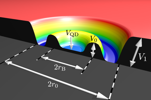
A cross section of a DRN with explanation of symbols used throughout the text is presented in Fig. 1.
The single–electron Hamiltonian in the presence of the in-plane magnetic field is written as
| (1) |
The confinement potential can be controlled by electrical gating which changes - the parameter describing the bottom of the inner QD potential. The energy spectrum of , calculated by numerical solving the Schrödinger equation, consists of a set of discrete states due to radial motion with radial quantum numbers , and rotational motion with angular momentum quantum numbers . To observe spin effects we assume that a large in-plane magnetic field is applied to DRN which has a negligible effect on orbitals, but causes substantial Zeeman splitting where is the spin gyromagnetic factor. The single particle wave function is of the form
| (2) |
with the radial part and the spin part . In our model calculations we take the radius of DRN nm, meV and set the zero potential energy at the level of , i.e., the potential well offset is equal . We consider here a case of a single electron trapped in DRN (although we have also discussed the many-particle states for i 16). The two lowest energy levels are ():
| (3) |
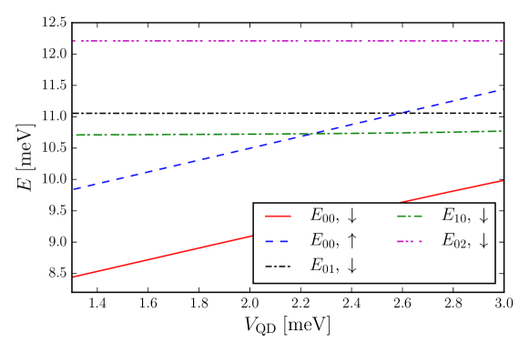
The energy spectrum as a function of in the absence of magnetic field is shown in Fig. 2.
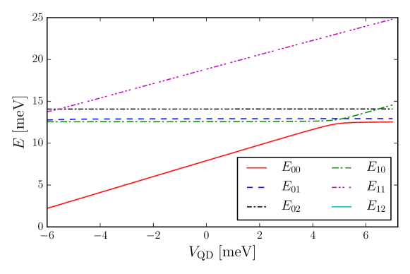
Depending on the shape of the confining potential, controlled by the value of , particular states are located in QD or QR part of the DRN. If a state is in the QD, its energy almost linearly increases with increasing , whereas the energies of states in the QR are not affected. In this manner even without the knowledge of the precise shape of the wave function one is able to determine if the electron is located in the QD or the QR.
3 Negative and Positive Differential Conductance
The system we study is a DRN weakly coupled via tunneling barriers to the source and drain electrodes with chemical potentials and , respectively. We estimate the sequential tunneling current from the source electrode through DRN to the drain electrode in the Coulomb blockade (CB) regime, i.e., the current is restricted to flow one electron at a time. To calculate the current we make use of the steady state solutions of rate equations11 for the average electron number at the -th energy state which is situated in the bias window , where is the bias voltage, and eventually obtain
| (4) |
Here, denotes all the quantum numbers of a particular state , (), are the Fermi–Dirac distribution functions for the electrodes (), , are the tunnel rates from the source electrode and to the drain electrode, respectively (calculated by Bardeen’s method 17). describes the change of the occupation of state due to relaxation processes. Namely, the occupation is increased by the relaxation from states higher in energy and decreased by relaxation to states with lower energy
| (5) |
where is the relaxation rate from state to state , is the total number of states and is the spin of an electron in state . The presence of ’s in the above equation means that we neglect relaxation processes between states with different spin orientation. As a result includes only the orbital relaxation, what will be explained below.
The DRN quantum states are assigned spin-down and spin-up. The transitions between these states, due to the coupling to the environment, strongly reflect their features. Namely, the relaxation rates of an excited state in nanostructures are very different if the transition involves () or does not involve spin flip ().18, 19 It was found both experimentally and theoretically that the relaxation rate between the energy states is much smaller than the orbital relaxation rate due to electron–phonon interaction ().11 Small () is responsible for the observation of long lived transient currents in nanostructures.20 calculated in Ref. 9 ranges from 10 Hz to Hz. Therefore, in the rate equations (4) we neglect the spin relaxation processes during the transport through the DRN.
To investigate spin related transport via DRN we design the system so that it can exhibit spin related negative differential conductance (NDC), i.e., the collapse of spin polarized current with an increase of the bias voltage. The reason of it is that the addition of a new conducting channel with smaller transmission probability effectively blocks the current and consequently . On the other hand, the addition of a new channel with larger transmission probability increases the current and one gets the increase of the current with an increase in the number of available channels, namely positive differential conductance (PDC) with . NDC region has attracted considerable attention due to its potential application in the realization of low power memory devices and logic circuits. NDC behavior is also known to offer great potential for high frequency applications as Bloch oscillators, frequency multipliers, and fast switching devices. 14, 12, 21
In this section we assume that QD and QR are made of different materials with the respective gyromagnetic factors , . We solve the Schrödinger equation in external magnetic field for a DRN with a position-dependent -factor. It is easy to estimate the energy of a particular state without any additional calculations, provided we know the energy spectrum of a homogeneous system presented in Fig. 2. When magnetic field is applied to a homogeneous system, its energies are shifted according to Eq. (3). However, in a DRN with different and factors, the Zeeman splitting is different in the QD and QR parts. It means that effectively an electron in the QD (QR) will “feel” an effective confining potentials
| (6) | |||||
| (7) |
Then, the difference between the bottoms of the QD and QR potentials is , where the sign “” (“”) corresponds to spin-up (spin-down) electrons. Since in the original problem we solve the Schrödinger equation for the confining potential with , we have to shift the energies by . Then, the spin-dependent energy spectrum for in external magnetic field can be approximately expressed by the spectrum for as follows
| (8) |
This formula means that in order to obtain the dependence of a particular energy of a spin-up (spin-down) electron on one has to shift the corresponding line in Fig. 2 up (down) by and to the left (right) by . This reasoning is approximate and valid only for , but at least qualitatively illustrates the effect of magnetic field.
We formulate below the conditions under which the arrangement of the spin energy levels is such that one gets spin related NDC or PDC. We distinguish two different situations of low bias regime where only the ground state lies in the bias window and high bias regime where also some excited states are in the bias. To show the idea we present below some analytical estimations of the ratio of the currents at high bias () and low bias () regimes,
| (9) |
and find the conditions under which (PDC) and (NDC). We also study the influence of unequal tunneling rates , on the discussed phenomenon (e.g. thicker barrier to the source electrode than to the drain electrode results in ). For simplicity in these analytical calculations we solve the rate equations for and consider only the two lowest energy levels. The currents calculated from the rate equations are:
| (10) |
| (11) |
where denote the ground and first excited energy states, respectively ( , or vice versa, see Figs. 4 and 6). To proceed with the analysis of the results we introduce the notation:
Parameter describes the ratio of the tunneling rates related to the thickness of the barriers to the drain and the source electrodes, whereas parameter reflects the mutual relation between the coupling strength of the higher and lower states to the electrodes. With this notation one finds
| (12) |
Let us discuss Eq. (12) in some limiting cases and look for the parameter regimes in which one finds PDC or NDC. This distinction is based on the relation between the values of the current in low and high bias regime described by the parameter.
It follows from these considerations that NDC can not be obtained if the electron enters DRN via thicker barrier and leaves DRN via the thinner one. In the other two cases one can find the parameter regime in which NDC occurs. We see that the decrease of the current is larger in the case of asymmetric barriers () than for the symmetric barriers (). The reason is that in the former case the thicker barrier to the drain electrode additionally blocks the transmission of the current. The relation between PDC and NDC regimes and the parameters and is summarized in Table 3.
Transport regimes defined by different values of the parameters and . \Hline (NDC) (PDC) (NDC) (PDC) (PDC) \Hline
We now illustrate the discussed phenomenon on two specific examples with two different sets of parameters. We present the results of the numerical calculations which take into account four lowest energy levels and all the subsequent orbital relaxation rates.
At first we consider DRN in which the inner QD has gyromagnetic factor and the outer QR has . In numerical calculations we assume T. The part of the energy spectrum that is crucial for switching between PDC and NDC is shown in Fig. 3. Spatial location of these states can be identified by their dependence on : as it was already mentioned, states situated in QD exhibit an increase in the energy with increasing , whereas those situated in QR have the energy (nearly) constant.
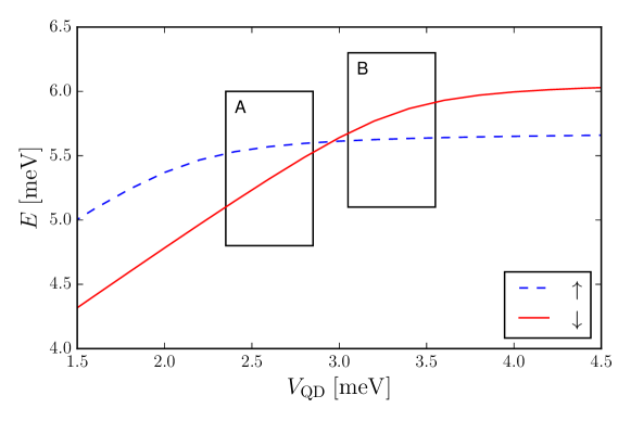
We can distinguish between different regimes signed in Fig. 3 with letters A and B in which we obtain spin related PDC and NDC, respectively.
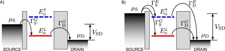
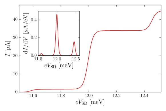
In panel A (the corresponding scheme is presented in Fig. 4A) the lowest energy state lies in the QD with very small tunnel coupling and the energy state is situated mostly in the QR with much larger . Therefore at low bias (only in bias window) we get weak, fully spin-down polarised current. At high bias ( and in the bias window, see Fig. 4B) an electron can tunnel also through a spin up channel which results in an increase in the total current with a small admixture of spin down current. We will refer to this current as partially spin polarized (Fig. 5). Consequently, in this case PDC takes place.
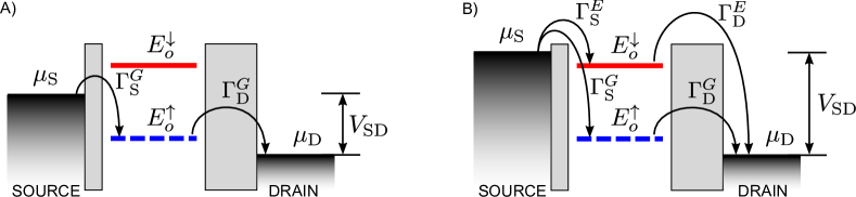
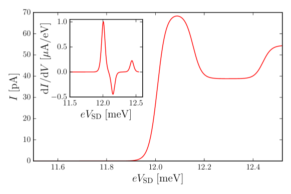
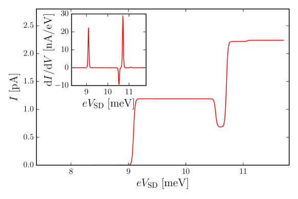
For larger , in regime marked by rectangle B in Fig. 3 (compare Fig. 6), the situation is different. The lowest energy state lies in the QR with large tunnel coupling whereas the state is situated mostly in QD with small . Therefore at low bias we get large, fully spin-up polarised current. At high bias ( and in the bias window) an electron entering the state effectively blocks the spin-up channel resulting in the decrease in the (partially spin polarised) current (Fig. 7), i.e., NDC occurs.
By changing one can switch DRN between PDC and NDC regimes.
As a second example let us assume that the inner QD is made of material with (e.g. InGaAs) and the outer QR is made of material with (e.g. InAs). The energy spectrum as a function of is presented in Fig. 8. and the dependence of the current (conductance) on the bias voltage with the pronounced NDC is shown in Fig. 9.
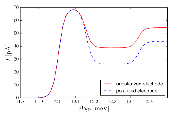
Finally, we consider the case illustrated in Fig. 6 but with the drain electrode being spin polarized (Fig. 10). As expected, in this case the NDC effect is stronger due to the simultaneous influence of the unequal tunneling rates of and states and thicker barrier for the spin-down electrons. It is shown in Fig. 10 as a dashed blue curve. For comparison for unpolarised electrodes is also presented as a solid red line.
4 Summary
Combined quantum structures are highly relevant to new technologies in which the control and manipulations of electron spin and wave functions play an important role. The ability to control the quantum state of a single electron is at the heart of many developments, e.g., in spintronics and quantum computing.
In contrast to real atoms, DRNs allow flexible control over the confinement potential which gives rise to wave function engineering. We have performed systematic studies of such manipulations on conducting properties of dot-ring nanostructures. In particular, we have shown that it is possible to design a structure which exhibits spin related positive or negative differential resistance and switch between them by changing the gate voltage. The results indicate an opportunity to tune the performance of nanostructures and to optimize their specific properties by means of sophisticated structural design. Thus, the basic issues of quantum mechanics can be explored to design new semiconductor devices in which specific properties can be optimized.
Acknowledgements
This work was supported by National Science Centre (NCN) under Grant No. DEC-2013/11/B/ST3/00824.
References
- 1 R. Hanson, L. P. Kouwenhoven, J. R. Petta, S. Tarucha, L. M. K. Vandersypen, Rev. Mod. Phys. 79, 1217 (2007).
- 2 J. M. Elzerman, R. Hanson, J. S. Greidanus, L. H. Willems van Beveren, S. De Franceschi, L. M. K. Vandersypen, S. Tarucha, L. P. Kouwenhoven Phys. Rev. B 67, 161308(R) (2003).
- 3 C. Somaschini, S. Bietti, N. Koguchi and S. Sanguinetti, Nanotechnology 22, 185602 (2011).
- 4 C. Somaschini and S. Bietti and N. Koguchi and S. Sanguinetti, Appl. Phys. Lett. 97, 203109 (2010).
- 5 L. J. Lauhon, M. S. Gudiksen, D. Wang, Ch. Lieber, Nature 420, 57 (2002).
- 6 D. C. Dillen, K. Kim, E. Liu, E. Tutuc, Nature Nanotechnology 9, 116 (2014).
- 7 P. K. Mohseni, A. D. Rodrigues, J. C. Gaizerani, Y. A. Pusep, R. R. Pierre, Journ. of Appl. Phys. 106, 124306 (2009).
- 8 A. Siusys, J. Sadowski, M. Sawicki, S. Kret, T. Wojciechowski, K. Gas, W. Szuszkiewicz, A. Kamińska, T. Story, Nanolett. 14, 4263 (2014).
- 9 E. Zipper, M. Kurpas, and M. M. Maśka, New J. of Phys.14, 093029 (2012).
- 10 M. Kurpas, E. Zipper, and M. M. Maśka, "Engineering of Electron States and Spin Relaxation in Quantum Rings and Quantum Dot-Ring Nanostructures" in "Physics of Quantum Rings", Vladimir M. Fomin (editor), Springer 2014, p. 455.
- 11 M. Kurpas, B. Kędzierska, I. Janus-Zygmunt, A. Gorczyca-Goraj, E. Wach, E. Zipper, M. M. Maśka, J. Phys.: Condens. Matter 27, 265801 (2015).
- 12 L. Britnell, R. V. Gorbachev, A. K. Geim, L. A. Ponomarenko, A. Mishchenko, M. T. Greenway, T. M. Frombold, K. S. Novoselov, , L. Eaves, Nature Communications 4, 1794 (2013).
- 13 T. Kostyrko, B. R. Bułka, Phys. Rev. B 79, 075310 (2009).
- 14 J. Chen, M. A. Reed, A. M. Rawlett, J. M. Tour, Science 286, 1550 (1999).
- 15 M. Ciorga, M. Pioro-Ladriere, P. Zawadzki, P. Hawrylak, A. S. Sachrajda, Appl. Phys. Lett. 80 2177 (2002); M.Ciorga et al., Phys. Rev. B 61, R16315 (2000).
- 16 A. Biborski, A. P. Kądzielawa, A. Gorczyca-Goraj, E. Zipper, M. M. Maśka, and J. Spałek, Sci. Rep. 6, 29887 (2016).
- 17 J. Bardeen, Phys. Rev. Lett. 6, 57 (1961).
- 18 U. Bockelman and G. Bastard, Phys. Rev. B 42, 8947 (1990).
- 19 A. V. Khaetskii and Y. V. Nazarov, Phys. Rev B 64, 125316 (2001).
- 20 T. Fujisawa, Y.Tokura, Y.Hirayama, Phys. Rev. B 63, 081304(R), (2001).
- 21 Y. Wu et al., ACS Nano 6, 2610 (2012).