InSe: a two-dimensional material with strong interlayer coupling
Abstract
Atomically thin, two-dimensional (2D) indium selenide (InSe) has attracted considerable attention due to large tunability in the band gap (from 1.4 to 2.6 eV) and high carrier mobility. The intriguingly high dependence of band gap on layer thickness may lead to novel device applications, although its origin remains poorly understood, and generally attributed to quantum confinement effect. In this work, we demonstrate via first-principles calculations that strong interlayer coupling may be mainly responsible for this phenomenon, especially in the fewer-layer region, and it could also be an essential factor influencing other material properties of -InSe and -InSe. Existence of strong interlayer coupling manifests itself in three aspects: (i) indirect-to-direct band gap transitions with increasing layer thickness; (ii) fan-like frequency diagrams of the shear and breathing modes of few-layer flakes; (iii) strong layer-dependent carrier mobilities. Our results indicate that multiple-layer InSe may be deserving of attention from FET-based technologies and also an ideal system to study interlayercoupling, possibly inherent in other 2D materials.
I INTRODUCTION
Isolation of graphene Novoselov et al. (2004); Geim and Novoselov (2007); Meyer et al. (2007) has triggered broad interest in the investigation of two-dimensional (2D) layered materials, such as hexagonal boron nitride (h-BN), Satta et al. (2001); Ishii and Sato (1983); Arya and D’Amico (1988) transition metal dichalcogenides (TMDCs)RadisavljevicB. et al. (2011); Novoselov et al. (2005); Yoon et al. (2011); Cai et al. (2014) and black phosphorus (BP).Li et al. (2016); Qiao et al. (2014); Hu et al. (2016) Recently, few-layer InSe as a post-transition metal chalcogenide has been synthesized via physicalFeng et al. (2014); Tamalampudi et al. (2014); Beardsley et al. (2016); Brotons-Gisbert et al. (2016); Mudd et al. (2013); Bandurin et al. (2017) and chemical methodsLei et al. (2014), exhibits promising characteristics for optoelectronic applications.Tamalampudi et al. (2014); Lei et al. (2014); Feng et al. (2015); Mudd et al. (2015); Balakrishnan et al. (2014); Lei et al. (2015); Camassel et al. (1978); Huo et al. (2017) High tunability in the band gap with varying layer thickness has been confirmed by experimental and theoretical investigations.Brotons-Gisbert et al. (2016); Mudd et al. (2013); Bandurin et al. (2017); Lei et al. (2014); Zólyomi et al. (2014); Errandonea et al. (2005); Gomes da Costa et al. (1993); Sánchez-Royo et al. (2014); Sun et al. (2016); Debbichi et al. (2015) In addition, carrier mobilities reaching or exceeding at room temperature have been reported,Feng et al. (2014); Bandurin et al. (2017); Segura et al. (1984); Sucharitakul et al. (2015) which are the highest among TMDCsCui et al. (2015); Fallahazad et al. (2016) and are superior to black phosphorus.Li et al. (2016); Qiao et al. (2014)
Previous experimental and theoretical studiesMudd et al. (2013); Bandurin et al. (2017); Lei et al. (2014); Gomes da Costa et al. (1993); Yang and Kelley (2005, 2006); E Kress-Rogers and G F Hopper and R J Nicholas and W Hayes and J C Portal and A Chevy (1983) on 2D InSe have already illustrated the evolution of electronic structure with thickness, which is generally attributed to quantum confinement effect,Mudd et al. (2013); Yang and Kelley (2005, 2006) a common feature observed in nanomaterials. In this paper, we calculate the electronic structure of -InSe and -InSe by employing ab initio density functional (DFT) calculations with long-range dispersion interaction in order to analyse broad variations in the band gap with changing layer thickness. We find that interlayer coupling in layered InSe is not as weak as generally believed to be the case in conventional van der Waals materials. Remarkably high electron distribution in the van der Waals gaps signal strong coupling between layers. We propose that interlayer coupling effect may be primarily responsible for the observed trends in the band gap of 2D InSe. We note that interlayer coupling, as a familiar effect in 2D materialsWu et al. (2015); Liu et al. (2014); Zhang et al. (2016); Chiu et al. (2014); Wang et al. (2016); Fang et al. (2014); Zhang and Zunger (2015); Wang et al. (2015); Zhang et al. (2017); Li et al. (2013); Chen et al. (2014); Dean et al. (2013); Yankowitz et al. (2012); Hunt et al. (2013); Ponomarenko et al. (2013) has been widely used in detecting layer thickness in multilayer graphene,Wu et al. (2015) realizing indirect-to-direct band gap transitions in TMDCsZhang and Zunger (2015); Wang et al. (2015); Zhang et al. (2017) and Hofstadter’s butterflyDean et al. (2013); Yankowitz et al. (2012); Hunt et al. (2013); Ponomarenko et al. (2013) in Graphene/-BN heterostructure. Here, we investigate several properties of 2D InSe associated with the interlayer coupling effect, including the magnitudes of band gap, band-edge positions, phonon frequencies, effective masses and carrier mobilities as a function of layer thickness. Our results offer new insight towards understanding the effects of interlayer coupling resulting in tunable band gap and thickness-dependent carrier mobility in few-layer InSe.
II METHOD
Density functional calculations are performed within the generalized gradient approximation (GGA) and Perdew-Burke-Ernzerhof (PBE) exchange-correlation functionalPerdew et al. (1996) as implemented in VASP code.Kresse and Furthmüller (1996, 1996); Kresse and Hafner (1993, 1994) The electron-ion interaction is described with projector-augmented plane wave (PAW) potentials.Kresse and Joubert (1999); Blöchl (1994) For all calculations, the plane-wave energy cutoff is set to 520 eV and the energy convergence threshold is set as . Monkhorst-Pack k-point meshes with spacing 0.03 are employed for the full relaxation of the geometry of layered -InSe and -InSe and uniform k mesh density is used when calculating band structures. The atomic flake and its neighbouring image are separated by a vacuum space that exceed 15 . For better accuracy, relaxations are performed including the van der Waals (vdW) interaction using optB86b-vdW and optB88-vdW functionals.Jiří Klimeš and David R Bowler and Angelos Michaelides (2010) The optimized structures obtained with optB86b-vdW functional for bulk -InSe and -InSe are both in excellent agreement with the experimental results (ESI Table S1). All subsequent calculations in this study are based on the optB86b-vdW functional. To ascertain the suitability of the DFT with GGA-PBE exchange-correlation, we have performed electronic structure calculations using several different approaches. For samples from monolayer to trilayer -InSe, we find that the higher-level hybrid density functional HSE06Krukau et al. (2006) GW+Bethe-Salpeter-Equation (GW+BSE, including excitonic electron-hole interaction)Albrecht et al. (1998); Rohlfing and Louie (1998), and GGA-PBE – all approaches – present similar trends in electronic band gap variations compared with experimental results (see ESI Figs. S1 and S2). Since, our focus is on the variation tendencies of band gaps and band-edge states with layer thickness, we trust that the GGA-PBE results do not affect the conclusions of this study, even though band gaps are underestimated. We calculate the optical phonon modes at the Brillouin Zone center () using linear response theory as implemented in the Quantum Espresso package.Paolo Gi (2009) These calculations are performed using norm-conserving pseudopotentials and a kinetic energy cutoff of 100 Ry. Density functional perturbation theory (DFPT)Baroni et al. (2001) is employed for the study of the vibrational frequencies at point for the atomic flakes.
On the basis of effective mass approximation, the carrier mobility in 2D materials is calculated by using the deformation potential (DP) theoryBardeen and Shockley (1950) and is expressed as:Cai et al. (2014); Sun et al. (2016); Takagi et al. (1994); Xu et al. (2016); Wang et al. (2014); Long et al. (2009); Bruzzone and Fiori (2011); Xi et al. (2012); Fiori and Iannaccone (2013); Price (1981); Xie et al. (2014):
| (1) |
Here, is the electron charge, is reduced Planck constant, is Boltzmann constant, and is the temperature (set to 300 K in this paper). represents the deformation potential constant of the valence band maximum (VBM) for hole or conduction band minimum (CBM) for electron along the transport direction, defined as . is energy change of the band under proper cell dilatation and compression, is lattice constant in the transport direction, and is the deformation of . is effective mass in the transport direction and is the average effective mass determined as . The elastic modulus of longitudinal strain along x and y directions of the longitudinal acoustic wave is derived from , where is the total energy and lattice volume at equilibrium for a 2D system.
III RESULTS and Discussion
III.1 Crystalline structure and electronic band structure of few-layer InSe.
Fig. 1a shows the top view of monolayer (ML) InSe, a quadruple Se-In-In-Se atomic sheet, where the relevant hexagonal primitive cell and orthogonal supercell are labeled with differently colored (black and magenta) frames. The corresponding first Brillouin zones of both primitive and supercell are shown in Fig. 1b. Two distinct structures (-InSe and -InSe) with different stacking patterns shown in Fig. 1c are selected for the following explorations. -InSe and -InSe consist of repeating bilayer and trilayer arrangements in the interlayer direction, respectively. Using first-principles calculations, we demonstrate in the following that the dependence of band gap with varying thickness is mainly dominated by interlayer coupling effect, and its impact on other properties of few-layer InSe.
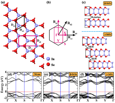
The calculated band structures of monolayer InSe with GGA-PBE functional and HSE06 functional are shown in ESI Fig. S1. Both functionals achieve consistent results with respect to band ordering and dispersion, but obtain different magnitude in the band gaps. The semi-local PBE functional is known to underestimate band gaps. Further test calculations on bilayer -InSe and trilayer -InSe using GGA-PBE, HSE06, and GW+BSE show similar trends (see ESI Fig. S2). Thus, we believe that PBE functional is able to precisely describe the band characteristics of few-layer InSe, while the band gaps are corrected by applying “scissors operator” to rigidly shift the conduction bands (CBs). Similar methodology has been employed in previous studies.Gomes da Costa et al. (1993); Parashari et al. (2008); Bernstein et al. (2002); Johnson and Ashcroft (1998); Fiorentini and Baldereschi (1995); A Thilagam and D J Simpson and A R Gerson (2011); Ramesh Babu et al. (2011) Here the uniform scissors operator, i.e., the band gap difference between the PBE and the HSE06 calculations for monolayer InSe, is adopted. The gap corrected PBE functional band structures of monolayer, bilayer -InSe and trilayer -InSe are presented in Fig. 1d-f.
III.2 Interlayer coupling evidenced by the evolution of band gaps and band-edge states with varying thickness of 2D atomic flakes.
It is known that multilayer graphene flakes have strong in-plane covalent bonds and weak interlayer interactions that show small layer-dependent band gap variations. However, from the -MLs stacked (with = 1-10), we find that the calculated gap values remarkably decrease with increasing layer thickness for the two polytypes of InSe as shown in Fig. 2a-b. The band gaps are about 2.39 eV for monolayer InSe and decrease to 1.24 eV and 1.18 eV for 10-MLs -InSe and -InSe, respectively. The sharp drops of 1.15 eV and 1.21 eV is comparable to other strongly coupled interlayer materials.Qiao et al. (2014); Zhao et al. (2016, 2017) The high tunability of band gap with varying thickness implies similarly strong interlayer coupling in the two polytypes considered here. Corresponding PBE band structures are listed in ESI Fig. S3 and Fig. S4, respectively. We also compare the calculated results with experimental data extracted from the energy peaks of photoluminescence (PL) spectroscopyMudd et al. (2013); Bandurin et al. (2017) in Fig. 2b. Evidently, our first-principles calculations (after applying scissors correction) agree well with the experimental results.Feng et al. (2014); Lei et al. (2014); Sánchez-Royo et al. (2014)
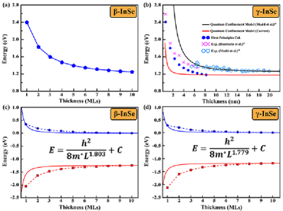
To further analyze the band gap diminutions, we assess the evolutions of the heights of the band edges with varying layer thickness as depicted in Fig. 2c-d. The heights of CBMs and VBMs are all aligned with respect to the corresponding vacuum levels, while the CBM of 10-MLs InSe is set to 0 eV for easy comparison. From the variation tendencies of CBMs (dashed blue lines) and VBMs (dashed red lines), we can see that both band edges contribute to the diminutions of band gaps as layer thickness increases. However, the height variations of VBMs are 2.28 and 2.46 times larger than those of CBMs for - and -InSe, respectively. This is to say that the band gap variations mainly rely on the upward shift of VBMs.
Previous studies attributed this dependence of the heights of energy levels on layer thickness to quantum confinement effect.Mudd et al. (2013); Yang and Kelley (2005, 2006) However, we found that a simple classical model based on quantum confinement effect does not appropriately explain the calculated data because the heights of band edges are inconsistent with those predicted with a weak coupling assumption. Under one-dimensional finite potential well model, when the band structures are solely dominated by the quantum confinement effect, the energy levels can be described as:
| (2) |
where, represents ground () and excited states (); is Planck’s constant; is the electron or hole effective mass along interlayer direction of bulk -InSe and -InSe and is the well width. Our calculated effective mass values (-InSe: 0.043 and 0.041 , -InSe: 0.032 and 0.035 ) are similar to those reported in previous works.Gomes da Costa et al. (1993); Kuroda and Nishina (1980); Kress-Rogers et al. (1982) In order to estimate , we define it as the projection distance along interlayer direction between two sideward Se atoms of InSe flakes with an additional 1 boundary. is the index (1.803 for -InSe and 1.779 for -InSe) and is a constant for alignment.
We firstly apply the one-dimensional finite potential well model to describe the band gap evolution with the layer thickness for -InSe (where the experimental data are available), as shown in Fig. 2b. Here the exciton reduced mass = (1/ + 1/ is evaluated as the input of in Eq. (2). For comparison, another model based on quantum confinement by Mudd et al.,Mudd et al. (2013) is shown in Fig. 2b. Both models fail to describe experimental gaps in the fewer-layer region. The implication is that quantum confinement may not be the sole factor controlling band gap evolution, and thus other effect, i.e., interlayer coupling, has to be included for a complete explanation.
The theoretical heights of CBMs and VBMs based on quantum confinement (i.e., the finite potential well model used here) are plotted as blue and red solid lines in Fig. 2c-d. Although the fitted (solid) curves roughly match the trends of first-principles calculated data (dashed curves), the results gradually deviate in the range of low thickness for both polytypes, indicating again that the one-dimensional finite potential well model is unable to describe the accurate height of band edges. Hence, the interlayer coupling effect should play an important role in the evolution of band gaps, especially the heights of VBMs in both InSe polytypes.
We should point out that although our above results indicate interlayer coupling may be an essential factor in determining the evolution of band-edge states, we should not completely abandon the concept of quantum confinement as the two effects are strongly intertwined, challenging to separate one from the other. This resembles the case of where quantum confinement and interlayer coupling coexist and in the fewer-layer region, the interlayer coupling stands out as a strong correction term.Zhang and Zunger (2015); Mak et al. (2010); Han et al. (2011); Kang et al. (2016)
III.3 Evolutions of the positions of band-edge states under strong interlayer coupling effect.
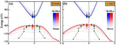
The lowest CB and the highest valence band (VB) of monolayer InSe shown in ESI Fig. S5 depict two nearly degenerate VBMs (within 1 meV) located along and directions, while the CBM is located at point. This indicates character of indirect band gap transition. From the evolutions of the lowest CBs and the highest VBs from monolayer to 10-MLs flakes as illustrated in Fig. 3, the CBMs remain at point and the band-edge shapes demonstrate kinetic energy release effect (strong dispersion) with increasing thickness in both InSe polytypes. The two nearly degenerate VBMs along and in monolayer InSe gradually shift towards point with increasing layer thickness. In other words, interlayer coupling brings a “lift” feature at point for VBMs that explains the indirect-to-direct band gap transition from monolayer to bulk structures. Similar transition is also observed in Phosphorene that has already been ascribed to strong interlayer coupling.Wang et al. (2015)
It should be noted that the effects of interlayer coupling is incorporated in our first principles calculations including weak van der Waals interaction. This is one reason why our calculated band gaps show good agreement with available experimental data (Fig. 2b). Apart from the earlier discussions, the existence of interlayer coupling in 2D InSe is further evidenced by the strong wave-function overlap between the band-edge states of adjacent layers, as shown in ESI Fig. S6. The effect is especially pronounced in the VBM states, consistent with the fact that the substantial deviation between quantum confinement model and first-principles data occurs to the VBM (see Figs. 2c-d).
III.4 Evolutions of the phonon frequencies under strong interlayer coupling effect.
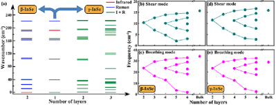
Both -InSe and -InSe have layer-dependent band gaps with drops of 1.15 eV and 1.21 eV from monolayer to 10-MLs, respectively. Such high tunability is the result of orbital hybridization in the interlayer region. In addition to the study of electronic properties, the detections of phonon modes at low frequency regions is already utilized to investigate interlayer interaction in 2D materials. Even in weakly coupled materials such as multilayer graphene, the variations of shear and breathing modes are the ideal tools to gauge flake thickness.Wu et al. (2015)
Fig. 4a shows the calculated frequencies and optical activities at point for few-layer InSe. Vibration modes are normally classified according to irreducible representation of the crystal symmetry. For the monolayer InSe, it retains a point group symmetry of owing to the presence of the horizontal reflection plane that average the In-In bonds. The corresponding representation is , where the two phonon modes are Infrared (I) active, the two modes are both Raman (R) and Infrared active, and the two and two are both Raman active as shown in ESI Fig. S7. The corresponding symmetry representations and optical activities for bilayer -InSe and -InSe are also illustrated in ESI Fig. S7, where the vibration modes are and , respectively. and are infrared active, and are Raman active, and and are both Raman and Infrared actives. The differences in optical activities between -InSe and -InSe could be ascribed to the different stacking patterns that cause the reductions of symmetry operators in -InSe.
Fig. 4b-e shows the calculated shear and breathing modes. The fan-like diagrams signify rapid frequency variations with increasing layer thickness. The separated frequencies retain the unique relationships with layer thickness in both -InSe and -InSe. In case of shear modes, the calculated frequencies (2-MLs 6-MLs) gradually descend from 10.37 to 3.11 for -InSe and from 11.51 to 2.80 for -InSe, respectively. The breathing mode frequencies vary from 23.51 to 1.76 for -InSe and from 23.35 to 2.31 for -InSe. These frequency variations are more than those reported in materials with strong interlayer coupling ( and ),Zhao et al. (2016, 2017) which suggests even stronger effect in InSe flakes. The differences in the breathing and shear mode frequency variations between -InSe and -InSe are indicative of distinct interlayer interactions in both polytypes. More specifically, it should be ascribed to the different overlapping of wave functions. As shown in Fig. 4b-e, interlayer coupling induces the fan-like frequency diagrams in both -InSe and -InSe, which has already been reported in twisted multilayer graphene with weak coupling.Wu et al. (2014)
III.5 Evolutions of the carrier mobilities under strong interlayer coupling effect.
From an engineering point of view, 2D InSe represents a promising semiconductor for electronic devices, such as the field-effect transistors (FET). Previous experimental studies on few-layer InSe revealed that the electron mobility reaches 1000 at room temperature,Feng et al. (2014); Bandurin et al. (2017); Segura et al. (1984); Feng et al. (2014) which is the highest reported value among TMDCsCui et al. (2015); Fallahazad et al. (2016) and is superior to black phosphorus.Li et al. (2016); Qiao et al. (2014) In this regard, the dependence of in-plane mobility on thickness is essential to device performance.
Here we utilize a phonon-limited scattering model to estimate the intrinsic carrier mobilities of InSe at different thicknesses, in which the primary scattering mechanism limiting carrier mobility is lattice phononsTakagi et al. (1994); Xu et al. (2016); Wang et al. (2014); Long et al. (2009); Bruzzone and Fiori (2011); Xi et al. (2012); Fiori and Iannaccone (2013); Price (1981); Xie et al. (2014) The carrier mobilities are not only controlled by the band-edge effective mass, but also by the 2D elastic modulus and the deformation potential. The elastic modulus and the band-edge deformation potential with respect to the vacuum energy are obtained by fitting strain-energy curves, as shown in ESI Fig. S8. All the calculated results of effective mass, deformational potential, 2D elastic modulus and carrier mobility are summarized in ESI Table S2 (-InSe) and Table S3 (-InSe) For InSe, the electrons usually exhibit higher mobility than holes for all thicknesses, because the VBs are generally much flatter than CBs (Fig. 3). The estimated electron mobility for monolayer InSe is 801.09 along direction and 689.20 along direction, while the hole mobility is only around 10 .
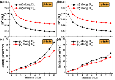
Fig. 5a-b shows he trend of inherent electron effective masses () as a function of layer thickness along the () and () directions. vidently, they gradually become small with increasing thickness, which is associated with the release process at point as the well-width increases. The electron conduction exhibits slightly anisotropic behavior, since the effective masses along are generally smaller than those along direction at all thickness for both - and -InSe. Fig. 5c-d shows the corresponding results of electron mobilities. As expected, they consistently increase with thickness. It is notable that the mobilities of -InSe are always higher than those of -InSe at any given thickness, which may be more favorable for electronic applications. As compared with the value of monolayer InSe, the mobility reaches about 10-30 k for 10-MLs, exhibiting an increase of 1-2 orders of magnitude. Such a large increase in mobility results mainly from the hardening of lattice caused by remarkably higher 2D elastic modulus of multi-layer InSe (see ESI Table S2 and Table S3). In this respect, we deduce that interlayer coupling is mainly responsible for the variation of strength of phonon scattering and would be a potential parameter available for mobility engineering in multi-layer 2D semiconductors.
IV CONCLUSIONS
By employing ab initio calculations including long-range dispersion interaction, we analyzed the evolution of electronic energies in -MLs stacked with number of layers = 1-10. The layer-dependent band gap values exhibit sharp drops 1.15 eV and 1.21 eV from monolayer to 10-MLs for -InSe and -InSe, respectively. A fitting with one-dimensional finite potential well model does not appropriately match the evolution of VBMs obtained by first-principles methods, implying that the changes in the band gap with layer thickness may not be dominated by quantum confinement effect. We surmise that strong interlayer coupling could be the primary cause which is manifested as following: first, the emergence of indirect-to-direct band gap transitions with increasing layer thickness; second, the fan-like frequency diagrams of shear and breathing modes and their variations with layer thickness derived from different interlayer interactions; finally, the layer-dependent carrier mobilities, whose values increase from about 0.80 k for the shared monolayer structure to 10-30 k for 10-MLs -InSe and -InSe, respectively. The considerably higher carrier mobilities of -InSe and -InSe along with their reduced band gaps should be desirable in electronic applications. With high band gap tunability and excellent transport properties, we speculate that -InSe and -InSe as strongly coupled layered 2D structures possess significant potential and deserve attention from FET industry.
Acknowledgements.
The authors acknowledge funding support from the National Natural Science Foundation of China (under Grant Nos. 11404131, 11674121, 61674080, and 61722403), Program for JLU Science and Technology Innovative Research Team, and the Special Fund for Talent Exploitation in Jilin Province of China. KB acknowledges support from US Department of Homeland Security under Grant Award Number, 2014-DN-077-ARI075.References
- Novoselov et al. (2004) K. S. Novoselov, A. K. Geim, S. V. Morozov, D. Jiang, Y. Zhang, S. V. Dubonos, I. V. Grigorieva and A. A. Firsov, Science, 2004, 306, 666–669.
- Geim and Novoselov (2007) A. K. Geim and K. S. Novoselov, Nature Materials, 2007, 6, 183–191.
- Meyer et al. (2007) J. C. Meyer, A. K. Geim, M. I. Katsnelson, K. S. Novoselov, T. J. Booth and S. Roth, Nature, 2007, 446, 60–63.
- Satta et al. (2001) G. Satta, G. Cappellini, M. Palummo and G. Onida, 00th International Workshop on Computational Materials Science, 2001, 22, 78–80.
- Ishii and Sato (1983) T. Ishii and T. Sato, Journal of Crystal Growth, 1983, 61, 689–690.
- Arya and D’Amico (1988) S. Arya and A. D’Amico, Thin Solid Films, 1988, 157, 267–282.
- RadisavljevicB. et al. (2011) RadisavljevicB., RadenovicA., BrivioJ., GiacomettiV. and KisA., Nat Nano, 2011, 6, 147–150.
- Novoselov et al. (2005) K. S. Novoselov, D. Jiang, F. Schedin, T. J. Booth, V. V. Khotkevich, S. V. Morozov and A. K. Geim, Proceedings of the National Academy of Sciences of the United States of America, 2005, 102, 10451–10453.
- Yoon et al. (2011) Y. Yoon, K. Ganapathi and S. Salahuddin, Nano Letters, 2011, 11, 3768–3773.
- Cai et al. (2014) Y. Cai, G. Zhang and Y. W. Zhang, Journal of the American Chemical Society, 2014, 136, 6269–6275.
- Li et al. (2016) L. Li, F. Yang, G. J. Ye, Z. Zhang, Z. Zhu, W. Lou, X. Zhou, L. Li, K. Watanabe, T. Taniguchi, K. Chang, Y. Wang, X. H. Chen and Y. Zhang, Nat Nano, 2016, 11, 593–597.
- Qiao et al. (2014) J. Qiao, X. Kong, Z. X. Hu, F. Yang and W. Ji, Nat Commun, 2014, 5, 4475.
- Hu et al. (2016) Z.-X. Hu, X. Kong, J. Qiao, B. Normand and W. Ji, Nanoscale, 2016, 8, 2740–2750.
- Feng et al. (2014) W. Feng, W. Zheng, W. Cao and P. Hu, Advanced Materials, 2014, 26, 6587–6593.
- Tamalampudi et al. (2014) S. R. Tamalampudi, Y.-Y. Lu, R. Kumar U., R. Sankar, C.-D. Liao, K. Moorthy B., C.-H. Cheng, F. C. Chou and Y.-T. Chen, Nano Letters, 2014, 14, 2800–2806.
- Beardsley et al. (2016) R. Beardsley, A. V. Akimov, J. D. G. Greener, G. W. Mudd, S. Sandeep, Z. R. Kudrynskyi, Z. D. Kovalyuk, A. Patanè and A. J. Kent, Scientific Reports, 2016, 6, 26970.
- Brotons-Gisbert et al. (2016) M. Brotons-Gisbert, D. Andres-Penares, J. Suh, F. Hidalgo, R. Abargues, P. J. Rodriguez-Canto, A. Segura, A. Cros, G. Tobias, E. Canadell, P. Ordejon, J. Wu, J. P. Martinez-Pastor and J. F. Sanchez-Royo, Nano Letters, 2016, 16, 3221–3229.
- Mudd et al. (2013) G. W. Mudd, S. A. Svatek, T. Ren, A. Patane, O. Makarovsky, L. Eaves, P. H. Beton, Z. D. Kovalyuk, G. V. Lashkarev, Z. R. Kudrynskyi and A. I. Dmitriev, Advanced Materials, 2013, 25, 5714–5718.
- Bandurin et al. (2017) D. A. Bandurin, A. V. Tyurnina, G. L. Yu, A. Mishchenko, V. Zolyomi, S. V. Morozov, R. K. Kumar, R. V. Gorbachev, Z. R. Kudrynskyi, S. Pezzini, Z. D. Kovalyuk, U. Zeitler, K. S. Novoselov, A. Patane, L. Eaves, I. V. Grigorieva, V. I. Fal’ko, A. K. Geim and Y. Cao, Nature nanotechnology, 2017, 12, 223–227.
- Lei et al. (2014) S. Lei, L. Ge, S. Najmaei, A. George, R. Kappera, J. Lou, M. Chhowalla, H. Yamaguchi, G. Gupta, R. Vajtai, A. D. Mohite and P. M. Ajayan, ACS Nano, 2014, 8, 1263–1272.
- Feng et al. (2015) W. Feng, J.-B. Wu, X. Li, W. Zheng, X. Zhou, K. Xiao, W. Cao, B. Yang, J.-C. Idrobo, L. Basile, W. Tian, P. Tan and P. Hu, Journal of Materials Chemistry C, 2015, 3, 7022–7028.
- Mudd et al. (2015) G. W. Mudd, S. A. Svatek, L. Hague, O. Makarovsky, Z. R. Kudrynskyi, C. J. Mellor, P. H. Beton, L. Eaves, K. S. Novoselov and Z. D. Kovalyuk, Advanced Materials, 2015, 27, 3760–3766.
- Balakrishnan et al. (2014) N. Balakrishnan, Z. R. Kudrynskyi, M. W. Fay, G. W. Mudd, S. A. Svatek, O. Makarovsky, Z. D. Kovalyuk, L. Eaves, P. H. Beton and A. Patanè, Advanced Optical Materials, 2014, 2, 1064–1069.
- Lei et al. (2015) S. Lei, F. Wen, B. Li, Q. Wang, Y. Huang, Y. Gong, Y. He, P. Dong, J. Bellah, A. George, L. Ge, J. Lou, N. J. Halas, R. Vajtai and P. M. Ajayan, Nano Letters, 2015, 15, 259–265.
- Camassel et al. (1978) J. Camassel, P. Merle, H. Mathieu and A. Chevy, Physical Review B, 1978, 17, 4718–4725.
- Huo et al. (2017) N. Huo, Y. Yang and J. Li, Journal of Semiconductors, 2017, 38, 031002.
- Zólyomi et al. (2014) V. Zólyomi, N. D. Drummond and V. I. Fal’ko, Phys. Rev. B, 2014, 89, 205416.
- Errandonea et al. (2005) D. Errandonea, A. Segura, F. J. Manjón, A. Chevy, E. Machado, G. Tobias, P. Ordejón and E. Canadell, Physical Review B, 2005, 71, 125206.
- Gomes da Costa et al. (1993) P. Gomes da Costa, R. G. Dandrea, R. F. Wallis and M. Balkanski, Physical Review B, 1993, 48, 14135–14141.
- Sánchez-Royo et al. (2014) J. F. Sánchez-Royo, G. Muñoz-Matutano, M. Brotons-Gisbert, J. P. Martínez-Pastor, A. Segura, A. Cantarero, R. Mata, J. Canet-Ferrer, G. Tobias, E. Canadell, J. Marqués-Hueso and B. D. Gerardot, Nano Research, 2014, 7, 1556–1568.
- Sun et al. (2016) C. Sun, H. Xiang, B. Xu, Y. Xia, J. Yin and Z. Liu, Applied Physics Express, 2016, 9, 035203.
- Debbichi et al. (2015) L. Debbichi, O. Eriksson and S. Lebegue, J Phys Chem Lett, 2015, 6, 3098–3103.
- Segura et al. (1984) A. Segura, F. Pomer, A. Cantarero, W. Krause and A. Chevy, Physical Review B, 1984, 29, 5708–5717.
- Sucharitakul et al. (2015) S. Sucharitakul, N. J. Goble, U. R. Kumar, R. Sankar, Z. A. Bogorad, F. C. Chou, Y. T. Chen and X. P. Gao, Nano Letters, 2015, 15, 3815–3819.
- Cui et al. (2015) X. Cui, G.-H. Lee, Y. D. Kim, G. Arefe, P. Y. Huang, C.-H. Lee, D. A. Chenet, X. Zhang, L. Wang, F. Ye, F. Pizzocchero, B. S. Jessen, K. Watanabe, T. Taniguchi, D. A. Muller, T. Low, P. Kim and J. Hone, Nat Nano, 2015, 10, 534–540.
- Fallahazad et al. (2016) B. Fallahazad, H. C. P. Movva, K. Kim, S. Larentis, T. Taniguchi, K. Watanabe, S. K. Banerjee and E. Tutuc, Physical Review Letters, 2016, 116, 086601.
- Yang and Kelley (2005) S. Yang and D. F. Kelley, The Journal of Physical Chemistry B, 2005, 109, 12701–12709.
- Yang and Kelley (2006) S. Yang and D. F. Kelley, The Journal of Physical Chemistry B, 2006, 110, 13430–13435.
- E Kress-Rogers and G F Hopper and R J Nicholas and W Hayes and J C Portal and A Chevy (1983) E Kress-Rogers and G F Hopper and R J Nicholas and W Hayes and J C Portal and A Chevy, Journal of Physics C: Solid State Physics, 1983, 16, 4285.
- Wu et al. (2015) J.-B. Wu, Z.-X. Hu, X. Zhang, W.-P. Han, Y. Lu, W. Shi, X.-F. Qiao, M. Ijiäs, S. Milana, W. Ji, A. C. Ferrari and P.-H. Tan, ACS Nano, 2015, 9, 7440–7449.
- Liu et al. (2014) K. Liu, L. Zhang, T. Cao, C. Jin, D. Qiu, Q. Zhou, A. Zettl, P. Yang, S. G. Louie and F. Wang, Nature Communications, 2014, 5, 4966.
- Zhang et al. (2016) J. Zhang, J. Wang, P. Chen, Y. Sun, S. Wu, Z. Jia, X. Lu, H. Yu, W. Chen, J. Zhu, G. Xie, R. Yang, D. Shi, X. Xu, J. Xiang, K. Liu and G. Zhang, Advanced Materials, 2016, 28, 1950–1956.
- Chiu et al. (2014) M.-H. Chiu, M.-Y. Li, W. Zhang, W.-T. Hsu, W.-H. Chang, M. Terrones, H. Terrones and L.-J. Li, ACS Nano, 2014, 8, 9649–9656.
- Wang et al. (2016) Z.-J. Wang, J. Dong, Y. Cui, G. Eres, O. Timpe, Q. Fu, F. Ding, R. Schloegl and M.-G. Willinger, Nature Communications, 2016, 7, ncomms13256.
- Fang et al. (2014) H. Fang, C. Battaglia, C. Carraro, S. Nemsak, B. Ozdol, J. S. Kang, H. A. Bechtel, S. B. Desai, F. Kronast, A. A. Unal, G. Conti, C. Conlon, G. K. Palsson, M. C. Martin, A. M. Minor, C. S. Fadley, E. Yablonovitch, R. Maboudian and A. Javey, Proceedings of the National Academy of Sciences, 2014, 111, 6198–6202.
- Zhang and Zunger (2015) L. Zhang and A. Zunger, Nano Letters, 2015, 15, 949–957.
- Wang et al. (2015) V. Wang, Y. C. Liu, Y. Kawazoe and W. T. Geng, The Journal of Physical Chemistry Letters, 2015, 6, 4876–4883.
- Zhang et al. (2017) C. Zhang, C.-P. Chuu, X. Ren, M.-Y. Li, L.-J. Li, C. Jin, M.-Y. Chou and C.-K. Shih, Science Advances, 2017, 3, .
- Li et al. (2013) Y. Li, Y. Rao, K. F. Mak, Y. You, S. Wang, C. R. Dean and T. F. Heinz, Nano Letters, 2013, 13, 3329–3333.
- Chen et al. (2014) Z. G. Chen, Z. Shi, W. Yang, X. Lu, Y. Lai, H. Yan, F. Wang, G. Zhang and Z. Li, Nat Commun, 2014, 5, 4461.
- Dean et al. (2013) C. R. Dean, L. Wang, P. Maher, C. Forsythe, F. Ghahari, Y. Gao, J. Katoch, M. Ishigami, P. Moon, M. Koshino, T. Taniguchi, K. Watanabe, K. L. Shepard, J. Hone and P. Kim, Nature, 2013, 497, 598–602.
- Yankowitz et al. (2012) M. Yankowitz, J. Xue, D. Cormode, J. D. Sanchez-Yamagishi, K. Watanabe, T. Taniguchi, P. Jarillo-Herrero, P. Jacquod and B. J. LeRoy, Nat Phys, 2012, 8, 382–386.
- Hunt et al. (2013) B. Hunt, J. D. Sanchez-Yamagishi, A. F. Young, M. Yankowitz, B. J. LeRoy, K. Watanabe, T. Taniguchi, P. Moon, M. Koshino, P. Jarillo-Herrero and R. C. Ashoori, Science, 2013, 340, 1427.
- Ponomarenko et al. (2013) L. Ponomarenko, R. Gorbachev, G. Yu, D. Elias, R. Jalil, A. Patel, A. Mishchenko, A. Mayorov, C. Woods, J. Wallbank and others, Nature, 2013, 497, 594–597.
- Perdew et al. (1996) J. P. Perdew, K. Burke and M. Ernzerhof, Physical Review Letters, 1996, 77, 3865–3868.
- Kresse and Furthmüller (1996) G. Kresse and J. Furthmüller, Computational Materials Science, 1996, 6, 15–50.
- Kresse and Furthmüller (1996) G. Kresse and J. Furthmüller, Physical Review B, 1996, 54, 11169–11186.
- Kresse and Hafner (1993) G. Kresse and J. Hafner, Physical Review B, 1993, 47, 558–561.
- Kresse and Hafner (1994) G. Kresse and J. Hafner, Physical Review B, 1994, 49, 14251–14269.
- Kresse and Joubert (1999) G. Kresse and D. Joubert, Physical Review B, 1999, 59, 1758–1775.
- Blöchl (1994) P. E. Blöchl, Physical Review B, 1994, 50, 17953.
- Jiří Klimeš and David R Bowler and Angelos Michaelides (2010) Jiří Klimeš and David R Bowler and Angelos Michaelides, Journal of Physics: Condensed Matter, 2010, 22, 022201.
- Krukau et al. (2006) A. V. Krukau, O. A. Vydrov, A. F. Izmaylov and G. E. Scuseria, The Journal of Chemical Physics, 2006, 125, 224106.
- Albrecht et al. (1998) S. Albrecht, L. Reining, R. Del Sole and G. Onida, Physical Review Letters, 1998, 80, 4510–4513.
- Rohlfing and Louie (1998) M. Rohlfing and S. G. Louie, Physical Review Letters, 1998, 81, 2312–2315.
- Paolo Gi (2009) Paolo Gi, Journal of Physics: Condensed Matter, 2009, 21, 395502.
- Baroni et al. (2001) S. Baroni, S. de Gironcoli, A. Dal Corso and P. Giannozzi, Reviews of Modern Physics, 2001, 73, 515–562.
- Bardeen and Shockley (1950) J. Bardeen and W. Shockley, Physical Review, 1950, 80, 72–80.
- Takagi et al. (1994) S. Takagi, A. Toriumi, M. Iwase and H. Tango, IEEE Transactions on Electron Devices, 1994, 41, 2357–2362.
- Xu et al. (2016) Y. Xu, J. Dai and X. C. Zeng, The Journal of Physical Chemistry Letters, 2016, 7, 302–307.
- Wang et al. (2014) Y. Wang, Y. Li and Z. Chen, The Journal of Physical Chemistry C, 2014, 118, 25051–25056.
- Long et al. (2009) M.-Q. Long, L. Tang, D. Wang, L. Wang and Z. Shuai, Journal of the American Chemical Society, 2009, 131, 17728–17729.
- Bruzzone and Fiori (2011) S. Bruzzone and G. Fiori, Applied Physics Letters, 2011, 99, 222108.
- Xi et al. (2012) J. Xi, M. Long, L. Tang, D. Wang and Z. Shuai, Nanoscale, 2012, 4, 4348–4369.
- Fiori and Iannaccone (2013) G. Fiori and G. Iannaccone, Proceedings of the IEEE, 2013, 101, 1653–1669.
- Price (1981) P. Price, Annals of Physics, 1981, 133, 217–239.
- Xie et al. (2014) J. Xie, Z. Y. Zhang, D. Z. Yang, D. S. Xue and M. S. Si, J Phys Chem Lett, 2014, 5, 4073–4077.
- Parashari et al. (2008) S. S. Parashari, S. Kumar and S. Auluck, Physica B: Condensed Matter, 2008, 403, 3077–3088.
- Bernstein et al. (2002) N. Bernstein, M. J. Mehl and D. A. Papaconstantopoulos, Physical Review B, 2002, 66, 075212.
- Johnson and Ashcroft (1998) K. A. Johnson and N. W. Ashcroft, Physical Review B, 1998, 58, 15548–15556.
- Fiorentini and Baldereschi (1995) V. Fiorentini and A. Baldereschi, Physical Review B, 1995, 51, 17196–17198.
- A Thilagam and D J Simpson and A R Gerson (2011) A Thilagam and D J Simpson and A R Gerson, Journal of Physics: Condensed Matter, 2011, 23, 025901.
- Ramesh Babu et al. (2011) K. Ramesh Babu, C. Bheema Lingam, S. Auluck, S. P. Tewari and G. Vaitheeswaran, Journal of Solid State Chemistry, 2011, 184, 343–350.
- Zhao et al. (2016) Y. Zhao, J. Qiao, P. Yu, Z. Hu, Z. Lin, S. P. Lau, Z. Liu, W. Ji and Y. Chai, Advanced Materials, 2016, 28, 2399–2407.
- Zhao et al. (2017) Y. Zhao, J. Qiao, Z. Yu, P. Yu, K. Xu, S. P. Lau, W. Zhou, Z. Liu, X. Wang, W. Ji and Y. Chai, Advanced Materials, 2017, 29, 1604230.
- Kuroda and Nishina (1980) N. Kuroda and Y. Nishina, Solid State Communications, 1980, 34, 481–484.
- Kress-Rogers et al. (1982) E. Kress-Rogers, R. Nicholas, J. Portal and A. Chevy, Solid State Communications, 1982, 44, 379–383.
- Mak et al. (2010) K. F. Mak, C. Lee, J. Hone, J. Shan and T. F. Heinz, Phys. Rev. Lett., 2010, 105, 136805.
- Han et al. (2011) S. W. Han, H. Kwon, S. K. Kim, S. Ryu, W. S. Yun, D. H. Kim, J. H. Hwang, J. S. Kang, J. Baik, H. J. Shin and S. C. Hong, Physical Review B, 2011, 84, 045409.
- Kang et al. (2016) J. Kang, L. Zhang and S.-H. Wei, J Phys Chem Lett, 2016, 7, 597–602.
- Wu et al. (2014) J.-B. Wu, X. Zhang, M. Ijäs, W.-P. Han, X.-F. Qiao, X.-L. Li, D.-S. Jiang, A. C. Ferrari and P.-H. Tan, Nature Communications, 2014, 5, ncomms6309.