The ESS FPGA Framework and its Application on the ESS LLRF System
Abstract
The functions of the Low-Level Radio Frequency (LLRF) system at European Spallation Source (ESS) are implemented on different Field-Programmable Gate Array (FPGA) boards in a Micro Telecommunications Computing Architecture (MTCA) crate. Besides the algorithm, code that provides access to the peripherals connected to the FPGA is necessary. In order to provide a common platform for the FPGA developments at ESS—the ESS FPGA Framework has been designed. The framework facilitates the integration of different algorithms on different FPGA boards. Three functions are provided by the framework: (1) Communication interfaces to peripherals, e.g. Analog-to-Digital Converters (ADCs) and on-board memory, (2) Upstream communication with the control system over Peripheral Component Interconnect Express (PCIe), and (3) Configuration of the on-board peripherals. To keep the framework easily extensible by Intellectual Property (IP) blocks and to enable seamless integration with the Xilinx design tools, the Advanced eXtensible Interface version 4 (AXI4) bus is the chosen communication interconnect. Furthermore, scripts automatize the building of the FPGA configuration, software components and the documentation. The LLRF control algorithms have been successfully integrated into the framework.
1 Introduction
By 2023, ESS will be the world’s most powerful neutron source in the world [1]. The neutrons will be produced by shooting protons to a heavy tungsten wheel in which the neutrons are produced by spallation. A nearly long linear accelerator will accelerate the protons to up to the required energy of . In the linear accelerator, the protons are accelerated by precisely synchronized Radio Frequency (RF) fields. Six different types of RF cavities are used at ESS to apply the RF field to the protons. The LLRF system is responsible to control the amplitude and phase of the RF field inside these cavities.
All low latency systems at ESS, which includes the LLRF system, will follow the MTCA standard [2]. The MTCA standard defines a computing system with a specific size of boards, the communication between the boards over a backplane and the management of the system by Intelligent Platform Management Interface (IPMI). So-called Advanced Mezzanine Carriers (AMCs) are inserted into an MTCA crate which realize different functions and build up a specific computing system. Generally, one of the AMCs is a Central Processing Unit (CPU) board that performs the central calculations and establishes a link to the upstream systems. Another common type of AMC is the FPGA board which allows application-specific functionalities to be implemented by them. The MTCA.4 extension of the standard adds enhanced possibility for rearside I/O connections and precision timing [3]. The rearside I/O connections are realized by plugging a separate board—the Rear Transition Module (RTM)—from the backside into the crate that is connected to the AMC by a dedicated connector.
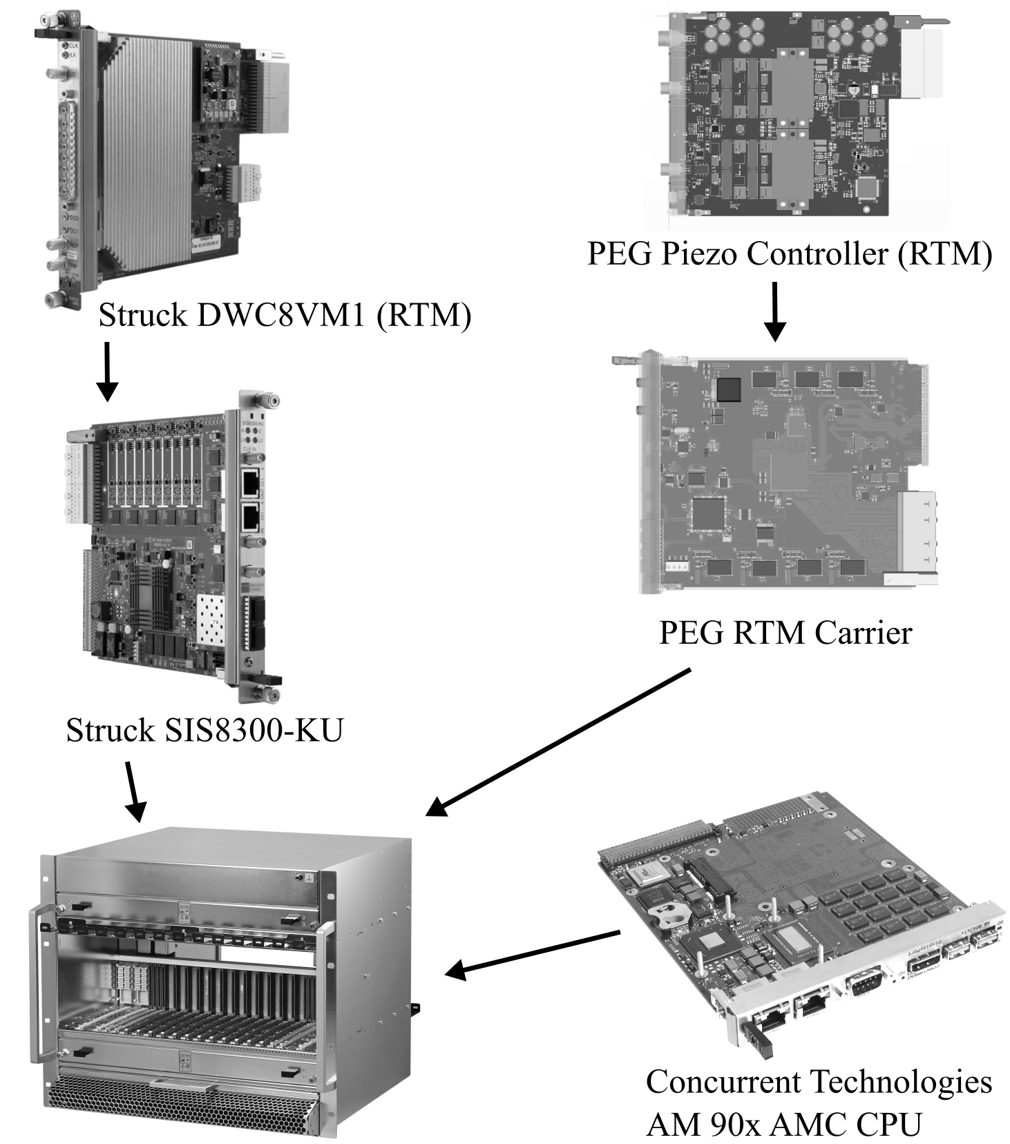
The LLRF controller of ESS is implemented on the FPGA of a Struck SIS8300-KU digitizer AMC [6]. Besides the control of the RF field, the piezo controller used to tune the frequency of the cavity is also part of the LLRF system at ESS [4]. The piezo controller is realized on an RTM developed by the Polish Electronics Group (PEG)—a collaboration between Polish universities and research centers [5]. To control the piezo controller, an FPGA AMC (PEG RTM carrier) has been developed by PEG. Figure 1 shows all the boards of a typical LLRF system at ESS that go into an MTCA crate. Other sub-systems of ESS also use the Struck SIS8300-KU.
All these applications implemented on an FPGA have to provide some common functionalities. These functionalities are for example: (1) Set parameters on the board and read the status from the board by the CPU in the crate over PCIe. (2) Acquisition of data and storage in a on-board memory. (3) Configuration of the board peripherals. For the same board, these functions are basically the same but also among different boards they require similar blocks of FPGA firmware. An FPGA framework is providing these functionality and allows the re-use of code among projects.
Frameworks that are provided by the board suppliers can only be implemented on their boards. On the other hand, available frameworks developed in the research community base a lot on own implementations of central elements like buses [7]. Therefore, the ESS FPGA Framework has been developed as a common platform for FPGA developments on different boards at ESS. To enable extensibility, the framework incorporates existing standards whenever possible.
2 Concepts of the Framework
The ESS FPGA Framework simplifies the implementation of FPGA applications for MTCA systems with a CPU in the crate. To make it easy to adapt the framework to different FPGA boards, board-specific parts are separated from common parts and the interfaces between those are well-defined. The same applies to the interface between the actual application and the framework. All project-specific changes are controlled by central configuration files.
On the one hand, it is important for a facility like ESS to receive support for the systems for several years. Therefore, solutions where the source code is not available and future support is uncertain should be avoided. On the other hand, it is expensive to develop all code from scratch. The tradeoff that the ESS FPGA Framework makes, is to follow open standards as far as possible. Specifically, the base communication infrastructure is based on AXI4—and open-standard, on-chip interconnect developed by ARM [8].
AXI4 is widely used and is also the standard interconnect to build up systems-on-chip in Xilinx Vivado [10]. This allows using Xilinx and third-party IP blocks within the framework. Many different functions are available in the IP repository of Xilinx [11]. Xilinx as the chip supplier has an interest in a living ecosystem around their FPGAs and, therefore, the availabilty of their IP blocks. Even if an own solution is preferred, such an IP block can help to get a first prototype of the system.
A common framework for different projects simplifies the development of the software on the upstream CPU. This affects the kernel driver as well as the access by the control system—Experimental Physics and Industrial Control System (EPCIS) in case of ESS [12]. The base of the software can be shared between the projects. Board- and project-specific parts can be added as modules.
Finally, the FPGA framework should integrate well with the workflow and tools used for software development at ESS. One example here is version control by git [13]. Many of these concepts are not yet widely used for FPGA developments but suit it well.
3 Structure of the Framework
The ESS FPGA Framework consists of different modules, which are illustrated in Figure 2. The application-specific functionality is contained within the custom logic which interfaces with the actual parts of the framework: the core framework and the data path. Whereas the core framework is the central part that controls the communication between the FPGA blocks and the external components as well as the upstream CPU. The components of the data path are responsible for the processing of high-speed and high-throughput data.

3.1 The Core Framework
Three functionalities are part of the core framework: the upstream communication to the CPU in the crate, the management of the on-board memory and the configuration of the board peripherals as described in the next section.
Within MTCA crates, PCIe is generally used for the upstream communication with a CPU board The upstream communication can be split into two different types. Two different interfaces are provided by the PCIe block of the ESS FPGA Framework for the two communication types.
Firstly, the CPU needs access to the on-board memory in order to transfer data from and to the board. An AXI4 interface with an additional Direct Memory Access (DMA) engine is directly connected to the memory controller of the framework. Secondly, parameters that control the functions on the board need to be set and the status of the board needs to be supervised. A separate AXI4-Lite interface enables the access to one or multiple register banks within the framework.
An AXI4 interconnect is used to combine and arbitrate the memory accesses from the different modules in the framework. A memory controller connected to the AXI4 interconnect realizes then the access to the on-board memory.
3.2 Configuration of the Board Peripherals
An essential functionality of the core framework is to configure the peripherals of the FPGA board. These peripherals could be for instance ADCs, Digital-to-Analog Converters (DACs), a clock generator or the clock distribution. Slow and simple serial protocols, such as Serial Peripheral Interface bus (SPI) and Inter-Integrated Circuit (I2C), are generally used for the configuration of these peripherals. Other components and functionalities are controlled by dedicated pins via a General-Purpose Input/Output (GPIO) interface.
In many projects, the configuration of the peripherals is controlled by the device driver running on the CPU in the crate. So after booting the system, the CPU in the system sends the configuration commands over registers on the board to dedicated interfaces in the FPGA. These interfaces issue the according signals to the configuration buses of the peripherals. As the used serial buses are not completely standardized, it is usually necessary to develop a specific firmware block to reflect the slighlty different behaviour of each peripheral.
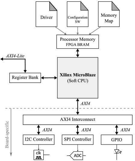
The board configuration is also rather static for most applications, i.e. it is not changed or just to a small extent during operation. Based on this static characteristic, the ESS FPGA Framework follows a different approach for the board configuration. The idea is to bundle all functionality that belongs to the board. The configuration of the peripherals goes together with the FPGA configuration rather than the board driver. For this reason, a small microcontroller system based on a Xilinx MicroBlaze soft-core [14] is included in the FPGA design that controls the configuration procedure. As a very basic setup of a MicroBlaze system is sufficient for executing the configuration, the penalty in terms of FPGA resources is small.
The software for the microcontroller is combined with the FPGA configuration (bit-file) and both together build the firmware of the board. This approach makes it easier to use the serial interface IP blocks provided by Xilinx because varieties in the protocols are easier to implement in the software of an on-chip controller than on the CPU of the crate. It also simplifies the driver development as the configuration software is implemented by the FPGA engineers who are more familiar with the hardware-specific functions. Nevertheless, the microcontroller is connected to the register bank and important board functions can be controlled by the CPU and the status of the peripherals can be read.
3.3 Data Path
For high-speed and high-throughput data exists a separate data path. The current implementation for the Struck SIS8300-KU digitizer uses the ADCs as the data source. After the source, the data is passed to a pre-processing block which is not board-specific. It is modular and may contain common functions such as filters, decimators and near-IQ sampling blocks. A set of compatible blocks is part of the framework. The pre-processing block contains also a memory interface through which raw or processed data can be stored directly in the on-board memory. The pre-processed data is routed to the custom logic and is finally sent to a sink which is a DAC in the current LLRF application.
To allow the highest throughput and real-time, a simple protocol with data signals and a data valid signal is used for the data path. To increase the consistency with the rest of the framework, the usage of the AXI4-Stream protocol is foreseen [9].
3.4 Integration of the Application—The Custom Logic
The actual FPGA application is embedded into a wrapper with well-defined interfaces towards the ESS FPGA Framework. Among other things, the wrapper defines interfaces for read and write access to the memory, inputs for data streams, and outputs for data streams.
Beside the defined interfaces, the custom logic also shares the register bank design with the framework. The custom logic contains its own instance of the register bank with its own register map but is connected to the same AXI4-Lite bus as the register bank of the framework. Thereby, the partitioning of the register bank is transparent to the driver. It is even possible to split up the custom logic register bank to multiple banks for different sub-blocks. The mapping of the different register banks to their corresponding addresses is handled by the design tools.
4 Automated Design Process
Along with the development of the ESS FPGA Framework, an automated workflow for FPGA projects has been developed. The goal of this workflow is to achieve repeatability throughout the whole design process. Therefore, developer A can take a version of a design and will get the same results that developer B got two weeks ago. Another goal of the automation is that the continuous integration tool Jenkins [16] can be used which is already part of the software integration at ESS.
4.1 Tools in the Workflow
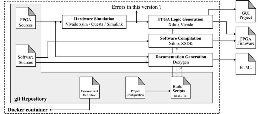
The whole process from the source code to the final design that can be loaded to the FPGA involves many different tools. Figure 4 shows the complete workflow with the tools involved.
To orchestrate the different tools, GNU make is applied—a tool widely used for build automation in software development [17]. GNU make is called with a certain goal that a developer wants to achieve. From its configuration, GNU make knows which scripts need to be called to achieve this goal. The scripts—written in languages like bash, Tcl and Python—control then the design tools. These scripts are also part of the project code.
The first step in the automated design process is the testing of the code by running test benches on a module, sub-system and system level. To allow the design process to be fully automated, the test benches need to be self-testing, i.e. no interaction by a designer is necessary to check the results. Only if the design passes all tests successfully, the generation of the FPGA configuration and the software for the configuration controller is executed. Tools supported for testing are, for instance, the Vivado simulator, Mentor Graphics Questa and Simulink. These tests are also part of the project code.
For the generation of the FPGA configuration, Xilinx Vivado is run in batch mode [18]. Vivado generates first the required IP blocks and block designs from their configuration. Afterwards, the scripts drive Vivado to execute all the steps from synthesis over place and route to the bit-file generation. During this process, Vivado stores all relevant information into report files. To allow a designer to analyze the system, a project is generated that can be opened in the Vivado Graphical User Interface (GUI).
In a similar way, Vivado XSDK compiles the software for the configuration controller [15]. Finally, both the bit-file and the software are bound to a single firmware file that can be loaded to the FPGA.
In parallel, doxygen is used to extract documentation about the modules and generate Hypertext Markup Language (HTML) files out of them [19]. This is done for Hardware Description Language (HDL) code as well as software. To include IP blocks and block designs in the documentation it is recommended to put the documentation into a HDL wrapper around the IP block.
Finally, to define the development environment the support for Docker containers will be added to the workflow. Docker can be understood as a lightweight version of a virtual machine. It defines an operating environment in which the software runs but does not need to start a complete virtual machine that occupies a lot of computer resources. For the automated design process, a Docker container could define for example the tool versions and environment variables.
4.2 Project Organisation
The code base of a project following the described design process is managed by the version control system Git [13]. As described before, the scripts which define how the output products of the project are generated are also part of the code. Therefore, the automated design process is also under version control and part of the project. The same applies to the test benches and test scripts. By including docker containers, even the development environment. The result is that everything that defines the project is under version control. This means that if a developer receives a version of the project, everything is included and the results can be reproduced as intended.
To achieve effective version control, a clean folder structure is necessary. Therefore, all files—sources, configuration files, scripts—are organized in a folder structure that is defined by the automated design process and does not follow the folder structure imposed by the design tools. A separate folder contains all the external modules and libraries that are used by the project. The number of files that belong to the project is kept to a minimum and all files that can be generated from other files should not be part of the code base. This is a general suggestion to make version control of the code work effectively. For instance, only the configuration files (.xci) of the Xilinx IP blocks are included in the project code as all the other files are re-generated by Xilinx Vivado. Most of the generated files such as reports from Xilinx Vivado, the software development workspace of Vivado XSDK or the Doxygen module documentation are placed in dedicated folders to clearly separate them from the files that go into version control.
5 Results and Resource Usage
A first version of the ESS FPGA framework with support for the Struck SIS8300-KU digitizer has been developed. The framework has been tested at a frequency of and for the central AXI4 interconnect.
As Table 1 shows, the resource usage is reasonable with most values around or below . Only the Block RAM (BRAM) usage going up to . With the applied configuration, debugging of the configuration controller software is possible on the board. By removing this possibility and optimizing the code for the configuration processor, the BRAM usage can decreased essentially.
| Resource | Utilization | Available | Util. |
|---|---|---|---|
| LUT | |||
| Flip-Flop | |||
| BRAM | |||
| DSP blocks | |||
| MMCM | |||
| PLL |
6 Conclusion
With the ESS FPGA Framework, a platform has been created that simplifies the FPGA developments for MTCA boards. Functionality that is needed for different projects is provided by this framework. As the framework interconnect is based on the AXI4 standard, IP blocks from other developers can be integrated and development time may be saved. The automated design process of the framework allows the FPGA designers to achieve repeatability of their results from testing over synthesis to integration. After the successful integration of the LLRF application, beam diagnostic applications at ESS are currently ported to the framework.
7 Acknowledgment
We would like to thank Struck Innovative Systeme GmbH for their support in the development of the ESS FPGA Framework.
References
- [1] S. Peggs et al., “Technical Design Report”, ESS, Lund, Sweden, ESS-2013-001, Apr. 2013.
- [2] Micro Telecommunications Computing Architecture Base Specification - PICMG MTCA.0 Revision 1.0, PICMG Standards, Jul. 2006;
- [3] MicroTCA.4 for Industry and Research: http://mtca.desy.de
- [4] A. J. Johansson et al., “LLRF System for the ESS Proton Accelerator”, in Proc. of the 5th Int. Accelerator Conf. (IPAC2014), Dresden, Germany, June 2014, paper WEPME079
- [5] J. Szewinski et al., “Contribution to the ESS LLRF System by Polish Electronic Group”, in Proc. of the 8th Int. Accelerator Conf. (IPAC2017), Copenhagen, Denmark, May 2017, paper THPAB129.
- [6] Struck - SIS8300-KU MTCA.4 Digitizer: http://www.struck.de/sis8300-ku.html
- [7] L. Butkowski et al., “FPGA Firmware Framework for MTCA.4 AMC Modules”, in Proc. 16th Int. Conf. on Accelerator and Large Experimental Control Systems (ICALEPCS2015), Melbourne, Australia, Oct. 2015, paper WEPGF074.
- [8] AMBA AXI and ACE Protocol Specification, ARM Specification, IHI0022E, 2013.
- [9] AMBA4 AXI4-Stream Protocol Specification, ARM Specification, IHI0051A, 2010.
- [10] AXI Reference Guide Xilinx, UG761, Mar., 2011.
- [11] Xilinx - Intellectual Property: http://www.xilinx.com/products/intellectual-property.html
- [12] EPICS - Experimental Physics and Industrial Control System: http://www.aps.anl.gov/epics
- [13] Git: http://git-scm.com
- [14] MicroBlaze Processor Reference Guide Xilinx, UG984-2017.1, Apr., 2017.
- [15] Vivado Design Suite User Guide Embedded Processor Hardware Design Xilinx, UG898-2017.1, May, 2017.
- [16] Jenkins: http://jenkins.io
- [17] GNU Make: https://www.gnu.org/software/make
- [18] Vivado Design Suite User Guide - Using Tcl Scripting Xilinx, UG894-2017.1, Apr., 2017.
- [19] Doxygen: http://doxygen.org