An Early Modeling Approach to Digital Electronics
Abstract
An Early modeling approach of transistors characterized by simplicity and accuracy in representing intrinsic non-linearities is applied to the characterization of propagation delay and level transition switching properties of NPN and PNP small signal transistors. Eight types of devices were considered, each represented by 5 samples taken from the same lot, totaling 20 NPN and 20 PNP transistors. Four switching time measurements were experimentally obtained, and the transistors also had their Early parameters (the Early voltage) and (a proportionality constant such that accurately estimated by using an experimental-numeric procedure that involves Hough transform accumulation in order to identify the crossing of the base current () indexed characteristic isolines, yielding the respective . The timing measurements exhibited strong positive Pearson correlations when taken pairwise. When these measurements were compared individually to the respective Early parameters, no significant Pearson correlation was obtained. However, a strong relationship was observed between the product of the two Early parameters and the ratio between the fall and rise time. A Pearson correlation coefficient of 0.78 was observed between these variables in the case of NPN devices. This suggests that transistors with larger average current gain tend to have more similar rise and fall times. The different relationship observed for PNP devices (Pearson 0.41) suggests some intrinsic difference in the way the Early parameters influence the rise and fall times of small signal transistors.
“You may delay, but time will not.’
B. Franklin
I Introduction
The most basic piece of information is the bit. Conceptualized by Claude Shannon in the 40s, the bit ended up constituting the basis of almost every computer machine nowadays, including all digital systems. In addition to its simplicity, digital representation and handling of information has the great advantage of being robust to noise.
While linearity represents the main objective of analog electronics, switching speed provides one of the main interests in digital electronics (e.g. roehr:1963 ; gray:1969 ; prasad:2009 ). As digital computing requires quick progress through a sequence of states, switching speed becomes the main factor limiting computing velocity. In general, it is the stray and intrinsic capacitances and inductances that limit switching speed by slowing down the digital transitions and implying in propagation delays. These effects are governed by respective time constants that, in the case of capacitance () is proportional to the time required to charge/discharge the capacitors. Interestingly, at this point digital electronics meets analog electronics, as these charging/discharging are inherently analog effects. Indeed, in a strict sense there is no purely digital electronics, as any state transition in the real-world requires an analog progression of values.
Transistors are the basis of modern electronics, both analog and digital. Though often simplified as being linear, transistors are actually highly non-linear devices. Most of these linearities stem of the geometric structure exhibited by the characteristic isolines. As a consequence of the Early effect (e.g. early:1952 ; jaeger:1997 ), these isolines cross one another, and with the (collector voltage) axis, at a well-defined point , where is the Early voltage. While the Early voltage has been considered in electronics, usually as a means to conceptualize the output resistance variation exhibited by transistors, and also as part of the Gummel-Poon model gummel:1970 ; moinian:2000 , it is not enough, when taken alone, to provide a complete description of the characteristics of junction transistors.
More recently, an approach has been reported that indicates that by incorporating a second, new proportionality parameter , it is possible to obtain a relatively accurate and yet simple model of transistors. The main advantage of this approach derives from the fact that neither or vary during the transistor operation. This is not the case with other transistor parameterizations, such as the traditional adoption of the current gain and output resistance , both of which vary with both and . Moreover, as the collector output resistance has been experimentally shown costaearly:2017 ; costaearly:2018 ; costaequiv:2018 to vary as , where is the base current, it becomes possible to derive a simple equivalent circuit costaequiv:2018 consisting of a fixed voltage source in series with a varying output resistance . As is typically very small, it is often possible to use the approximation . Interestingly, the average current gain can be approximated as . Observe that it was precisely the introduction costaearly:2017 ; costaearly:2018 of the proportionality parameter that not only provided a direct indication of the output resistance , but also allowed the Early voltage to be related to the average current gain .
This approach relying on the Early voltage and the complementary proportionality constant has been called the Early model of small signal transistors costaearly:2017 ; costaearly:2018 ; costaequiv:2018 . This approach has been successfully applied to a number of important problems in analog electronics. First, it allowed several real-world silicon and germanium junction small signal transistors, of types NPN and PNP, to be mapped into the space costaearly:2018 ; germanium:2018 ; costaequiv:2018 , defining a prototype distribution of the four groups in the Early parameter space. This revealed that NPN types have smaller parameter variation, while being characterized by larger magnitudes and smaller values of . However, the centers of mass of both NPN and PNP silicon groups resulted very near the current gain isoline , the same being observed for the germanium NPN and PNP groups, but with in this case. Silicon and germanium transistors tended to “gravitate” along two respective “belts” along the respective current gain isolines. Interestingly, almost negligible overlap has been verified between the NPN and PNP groups, be it regarding silicon or germanium devices. These results show that real-world transistors have intrinsic specific properties that influence their linearity, output resistance and, therefore, performance in amplification.
The above results motivated the proposal of an Early equivalent model costaequiv:2018 , which consists of a fixed voltage source in series with a variable output resistance . This equivalent circuit allowed the mathematical analysis of a simplified common emitter configuration costaequiv:2018 , as well as the more complete configuration including negative feedback commemitt:2018 . In the latter case, it was possible to derive equations for the gains, leading to an accurate analysis of the effects of the and parameters on current and voltage gains, as well as the implied non-linearities. Other related developments include the analysis of capacitive loads on amplification costareact:2018 .
The efficacy of the Early approach to characterize and analyze analog circuits motivates its possible extension to digital electronics. In particular, would it be possible to correlate the and parameters with propagation delays and switching transistors? If so, the Early approach could be extended to the characterization of the switching properties of real-world transistors, paving the way to several applications as well as analytical investigations. This provides the main motivation for the present work.
We start by briefly revising the Early modeling approach, and then present some basic principles regarding the characterization of switching properties. Following, experimental measurements of the delay and transition switching times, and then of and parameters are presented and related one another. Interesting results are then presented and discussed, and the article concludes by outlining prospects for further related research.
II Brief Review of the Early Modeling Approach
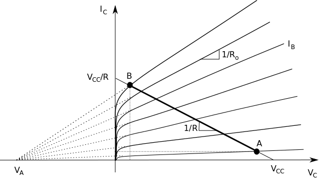
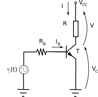
Figure 1 depicts the Early approach to modeling small signal transistors while taking into account the respective non-linearities. This refers to the “common emitter” circuit configuration shown in Figure 2. The space corresponds to the operation space of the transistor, which is restricted by the purely resistive load to excursion along the load line passing through the points and . A characteristic isoline curve is defined for each value of the base current , and these isolines intersect at the point along the axis, where is the Early voltage. The circuit excursion is, however, limited by the cut-off (point ) and saturation (point ) regions of the transistor. The tangent of each isoline corresponds to the reciprocal of the collector output resistance .
The Early modeling of the circuit in Figure 2 yields the following current and voltage equations:
| (1) | |||
| (2) |
Observe that the collector output resistance is a function of , i.e. . Thus, despite the extreme simplicity of these equations, they are still capable of incorporating, to a good level of accuracy, the amplification non-linearity implied by the converging isolines.
In the case of the input mesh, we take the traditional approach , where is the fixed offset ( for silicon) and is the input resistance.
Given a transistor, its parameters and can be easily estimated through a experimental-numeric procedure costaearly:2018 . First, the characteristic isolines are acquired by making and measuring for . This can be conveniently achieved by using a microcontrolled system costaearly:2018 . Once the isolines have been obtained and conditioned costaearly:2018 , respective straight lines are estimated by using minimum squared linear regression. The determination of the intersection of these lines can then be effectively accomplished by using a Hough transform accumulation scheme costaearly:2018 , which allows eventually diverging isolines not to interfere with the peak of the intersections. The proportionality parameter can be easily obtained by linear regression of the angle of the obtained isolines in terms of . This procedure has been verified costaearly:2018 ; germanium:2018 ; costaequiv:2018 , for hundreds of small signal silicon and germanium transistors, to yield an accurate and stable estimation of both and .
It is interesting to recall that the above outlined Early modeling approach of transistors and related circuits derives part of its simplicity from the experimentally verified costaearly:2017 ; costaearly:2018 tendency of to vary linearly with through , i.e. . This approach can be adapted in cases where this dependence may follow a different relationship.
III Switching Measurements
There are at least two main types of switching effects to be considered in digital electronics: (i) propagation delays; and (ii) transition times. Figure 3 shows the input digital signal (in red) and the respective output (in green). Four switching measurements can be defined: (a) the propagation delay from low to high levels; (b) the rise time ; (c) the propagation delay from high to low levels; and (d) the fall time .
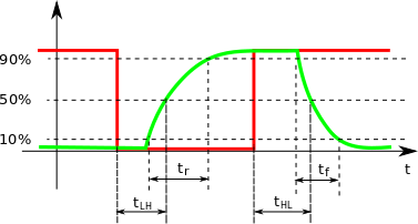
So, given a switching circuit such as that in Figure 2, an input signal can be driven into it, and the above mentioned four measurements obtained by using a logging system or a digital oscilloscope.
IV Experimental Set-Up
Eight types of small signal silicon transistors (4 NPN and 4 PNP) were considered, each represented by 5 respective samples taken from the same lot. These devices are all in plastic package (TO-92) and correspond to models commonly used in discrete electronics. First, these transistors had their Early parameters and estimated by using the methodology summarized in Section II. Then, they were mounted in the circuit configuration shown in Figure 2, having , , and . The input signal was a square wave derived from a signal generator, with and . Both the input and the output signal were monitored with a digital oscilloscope, so that the adopted four switching times could be estimated. For simplicity’s sake all the currents and voltages of PNP transistors are henceforth shown with inverse signs, allowing these devices to be discussed in the same way as the NPN counterparts.
V Switching Time Results
Figure 4 shows the scatterplots obtained for (a) ; (b) ; (c) ; and (d) . Interestingly, all these cases yielded high positive Pearson correlations, with the two cases involving – i.e. (a) and (d) – leading to particularly high correlation values. These results indicate that the considered delay and transition times are all interrelated. However, observe that the positive transitions (i.e. and ) have markedly different values from the negative transitions (i.e. and ). Actually, the latter take place about 4 times faster than the former. This suggests that the adopted transistors in the considered circuit configuration can drain the stray capacitances much faster than charging them.
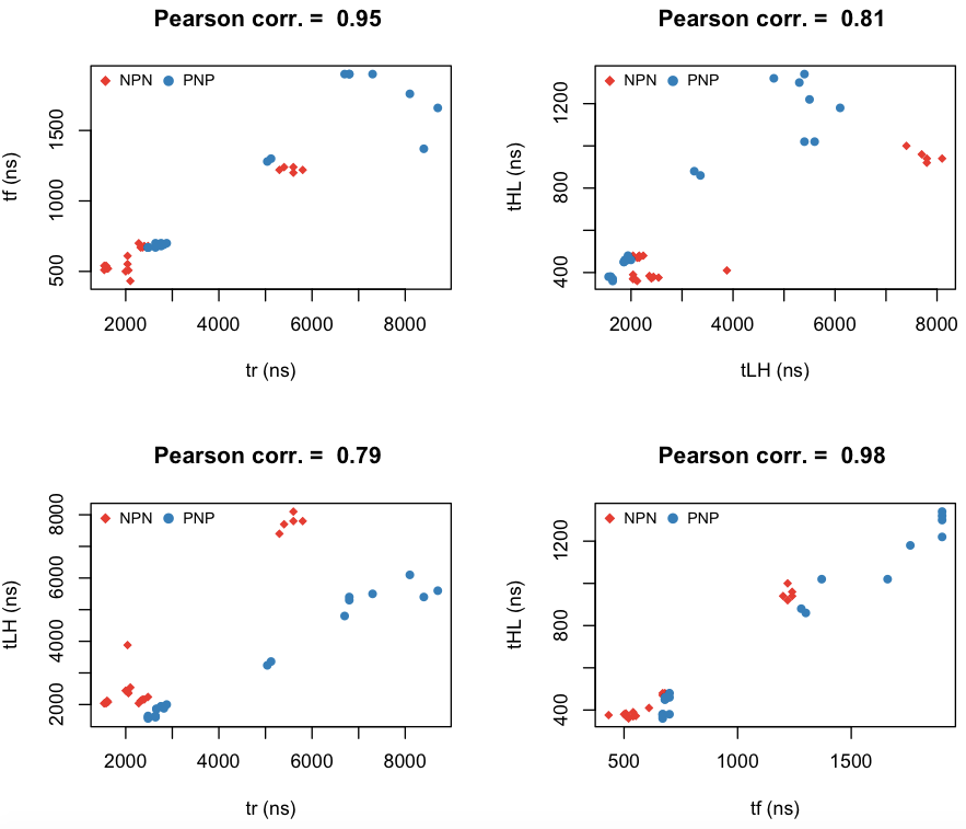
The scatterplots in Figure 4 also identify the two types of considered transistors, i.e. NPN and PNP. No special relationship can be identified in any of the 4 scatterplots regarding these two types.
VI Early Parameters Estimation
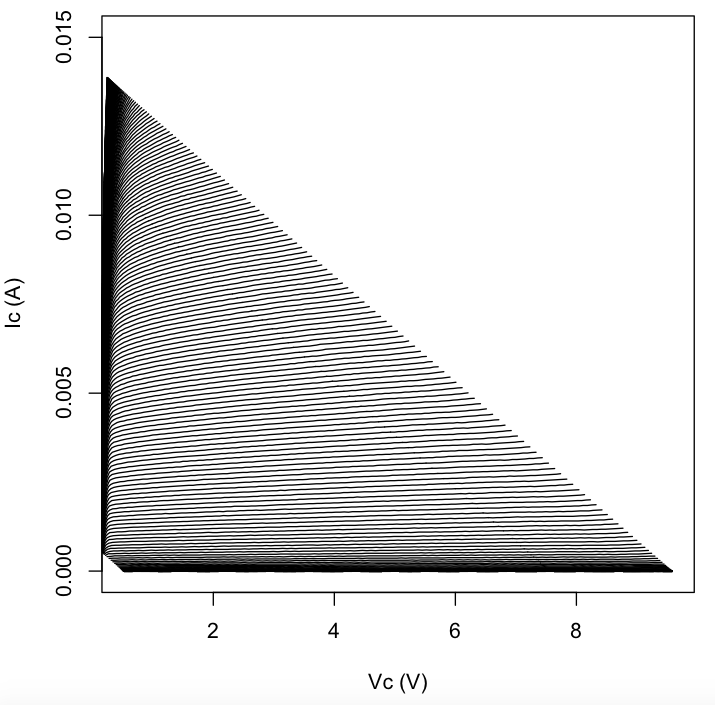
The characteristic isolines typically obtained for the considered transistors are illustrated in Figure 5. Great attention to shielding and isolation of the digital and analog modules of the acquisition system costaearly:2018 allowed high noise immunity and data quality, which contributed to more accurate estimation of the Early parameters and . The fanning structure of the isolines typically found in real-world transistors are evident in this figure. They are the main source of transistor amplification non-linearity. Observe the cut-off and saturation regions.
The characteristic isolines obtained experimentally for each transistor were processed by the Early estimation procedure as described above, so that each transistor could be characterized in terms of its respective parameter configuration , which are mapped into the henceforth called Early space. Figure 6 shows the distribution of all 40 transistors (20 NPN and 20 PNP) in the Early space, showing also the average current gain isolines respectively to (in bottom-up direction).
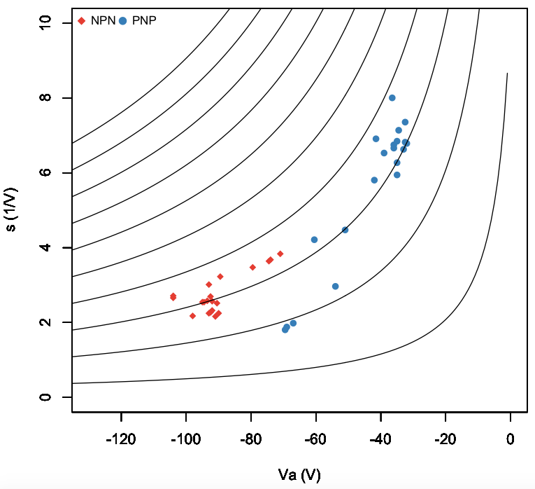
Several interesting features can be observed in Figure 6. First, we have that, with a few exceptions observed for PNP devices, most transistors resulted inside the current gain belt , with the isoline being very near the center of mass of the two groups of devices. This is in complete agreement with previous studies costaearly:2018 ; germanium:2018 , corroborating this as the region likely occupied by small signal transistors. The PNP transistors have smaller magnitudes of and higher values of , exhibiting almost no overlap with the NPN counterparts. This overall organization of NPN and PNP small signal transistors in the Early space has been called the prototypical space of transistors costaearly:2018 . The region has been found to be populated by alloy junction germanium transistors germanium:2018 , the region of the Early space such that seems to be empty of real-world transistors, except possibly for Darlington configurations. This region of high average current gain is also characterized by large values of , as a consequence of the nearly “concentric” geometrical organization of the current gain isolines, reaching a peak (in this diagram) of gain, magnitude and at the point .
VII Relationship between Switching Times and Early Parameters
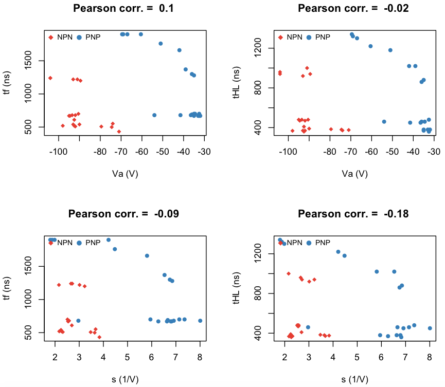
Having experimentally estimated the four switching times and the respective Early parameters for each of the 40 transistors, we are now in position to study the interrelationship between these characteristics. Figure 7 shows four of the possible correlations between the 4 time measurements and the 2 Early parameters. Remarkably, no significant correlation can be identified. This suggests complete absence of relationships between the considered delay and transition time measurements and the Early parameters, at least as long as these measurements are considered isolately.
However, it is also interesting to consider combinations between the adopted measurements, such as respective products and ratios. Figure 8(a) depicts the scatterplot of . Recall that . Interestingly, a moderate positive correlation (0.41) is obtained in this case. However, it can be discerned in this same scatterplot that the NPN and PNP devices follow different relationships, with the former exhibiting a more definite positive correlation. Figures 8(b) and (c) shows the scatterplot separately only for PNP (b) and NPN (c) transistors, which yielded respective Pearson correlations of and . So, the NPN indeed leads to a much more definite relationship , with a very significant correlation coefficient. This means that the ratio can be estimated with relatively good accuracy from the product . The larger this product, the larger will be relatively to . Figure 8(d) shows the relationship between and , which is also characterized by a moderate positive Pearson correlation of .
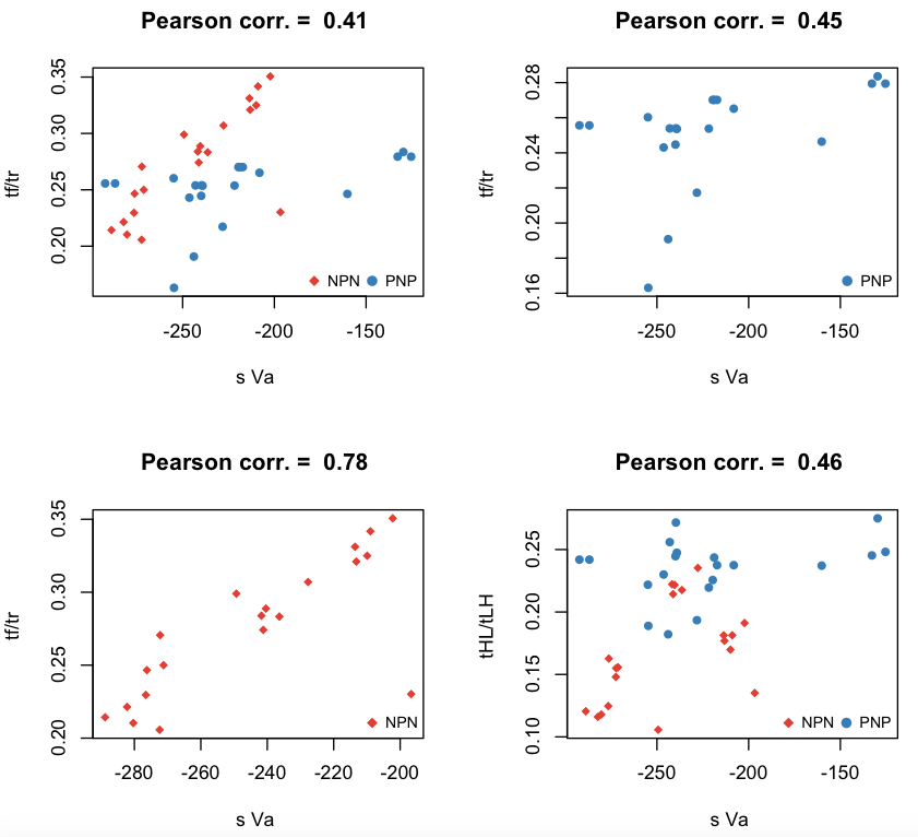
can be, in the average, estimated with good accuracy from the product of Early parameters .
So, though no direct relationship can be identified between the four delay and transition times measurements and the two Early parameters taken isolately, a relatively strong relationship ultimately appeared when considering the product and the ratio . The obtained positive correlation indicates that more symmetrical transitions and are obtained for larger values of . This makes sense because larger current gains will contributed to charging the stray capacitances faster, therefore reducing relatively to and yielding larger ratios . Interestingly, the average current gains typically observed for silicon NPN and PNP devices (i.e. ) can lead to a maximum ratio of about . The symmetric configuration between the rise and fall times, characterized by cannot be obtained even for the transistors with peak magnitude, which limits to . Thus, NPN and PNP small signal transistors when used in the adopted circuit configuration (and also likely in other related circuits) have intrinsic ratios that are substantially smaller than 1, being therefore characterized by fall times much smaller than rise times, at least for the considered devices and circuit configuration.
As both Early parameters and do not reflect any property of the base-emitter transistor junction, it follows that the observed relationship is mostly concerned with capacitances in parallel with . The fact that this relationship was almost twice larger for NPN than PNP transistors suggests some intrinsic difference regarding the switching properties of these two types of transistors.
VIII Concluding Remarks
The switching properties of transistors, may they be related to propagation delays or level transitions, critically define the speed of digital switching circuits. In the present work, we applied a recently Early modeling approach to transistors costaearly:2017 ; costaearly:2018 ; germanium:2018 ; costaequiv:2018 , characterized by great simplicity allied to accuracy in representing the transistor non-linearities, as a possible means to study switching properties of small signal NPN and PNP silicon bipolar junction transistors.
Four time measurements were considered for characterizing the transistor switching properties: rise time , fall time , transition from low to high levels , and transition from high to low levels . The transistor amplifying characteristics and intrinsic non-linearities stemming from the converging characteristic isolines were effectively summarized in terms of the Early parameters and . The time measurements were determined by using a digital oscilloscope, while the Early parameters were obtained by an accurate experimental-numeric, approach previously described costaearly:2018 that uses Hough transform accumulation in order to identify the intersection of the base current-indexed isoline characteristics implied by the Early effect.
The switching time measurements were found to correlate strongly one another, especially in those cases involving f. The Early characterization was in full agreement with results previously obtained with respect to NPN and PNP small signal silicon transistors costaearly:2018 , defining two respective clusters in the Early space . NPN transistors are characterized by larger magnitude and smaller parameter values than PNP transistors. The average current gain obtained for these two groups are both very similar to 250.
The 4 considered switching times exhibited substantial positive Pearson correlation, with the cases involving resulting in particularly strong correlation values. When the switching times were individually compared with the Early parameters and , no appreciable Pearson correlation could be identified. However, a significant positive Pearson correlation was observed between the variables and the ratio . This correlation resulted much stronger (0.78) for NPN transistors than their PNP counterparts (0.45), suggesting an intrinsic difference in the relationship between the switching and Early properties of these two types of small signal silicon transistors. It is interesting to observe that the valued estimated as does not necessarily coincides with the values found in data sheets or obtained by using more traditional approaches. Indeed, results from the accurate estimation of by identification of the isolines characteristics intersection, while is obtained by linear regression of the isoline angles and the base current .
Interestingly, the ratio is significantly smaller than 1 for both NPN and PNP types, implying an inherent switching asymmetry. This asymmetry is reduced for transistors with larger , but the maximum ratio obtained for the considered devices was limited to . The fact that NPN and PNP silicon transistors seem to have implies it to be in principle impossible, at least for the considered devices and circuit configuration, to reach perfect symmetry between the rise and fall times. A similar, even though less defined situation holds concerning the ratio . Interestingly, in this case no difference resulted regarding the relationship between the times and Early parameters with respect to the NPN and PNP transistors.
All in all, the results obtained respectively to the considered transistor types and circuit configuration revealed several interesting results and trends. In particular, it was shown that the ratio can be predicted with relatively good accuracy from the product of Early parameters of the respective transistor, especially in the case of NPN devices. This approximation can contribute to both practical and theoretical studies of transistors used as switches.
Several possibilites of further investigations have been defined by the reported approach and respective results, including the extension to other types of transistors and circuits, Darlington configurations, and power switching. It would also be interesting to explain the observed relationships and effects in more theoretical terms.
Acknowledgments.
Luciano da F. Costa thanks CNPq (grant no. 307333/2013-2) for sponsorship. This work has benefited from FAPESP grants 11/50761-2 and 2015/22308-2.
References
- (1) WD Roehr. High Speed Switching Transistor Handbook. Motorola, 1963.
- (2) P. E. Gray and C. L. Searle. Electronic Principles: Physics, Models and Circuits. John Wiley and Sons, 1969.
- (3) S. Prasad, H. Schumacher, and A. Gopinath. High Speed Electronics and Optoeletronics: Devices and Circuits. Cambridge University Press, 2009.
- (4) J.M. Early. Effects of space-charge layer widening in junction transistors. Proceedings of the IRE, (11):1401–1406, 1952.
- (5) R. C. Jaeger and T. N. Blalock. Microelectronic Circuit Design. McGraw-Hill New York, 1997.
- (6) H. K. Gummel and H. C. Poon. An integral charge control model of bipolar transistors. Bell Syst. Tech. J., 49:827–852, 1970.
- (7) C. Xiaochong, J. McMacken, K. Stiles, P. Layman, J. J. Liou, A. Ortiz-Conde, and S. Moinian. Comparison of the new VBIC and conventional Gummel-Poon bipolar transistor models. IEEE Trans. Electronic Devs., 47(2):427–433, 2000.
- (8) L. da F. Costa, F.N. Silva, and C.H. Comin. An Early model of transistors and circuits, 2017. arXiv preprint arXiv:1701.02269.
- (9) L. da F. Costa. Characterizing complementary bipolar junction transistors by early modeling, image analysis, and pattern recognition, 2018. arXiv preprint arXiv:1801.06025.
- (10) L. da F. Costa. Towards a simple, and yet accurate, transistor equivalent circuit and its application to the analysis and design of discrete and integrated electronic circuits, 2018. https://archive.org/details/reactive_201802.
- (11) L. da F. Costa. Characterizing germanium junction transistors, Jan. 2018. https://archive.org/details/Germanium.
- (12) L. da F. Costa. Analysis of the common emitter amplifier taking into account transistor non-linearity, Feb. 2018. archive preprint https://archive.org/details/comm_emitt.
- (13) L. da F. Costa. On the effects of resistive and reactive loads on signal amplification, Feb 2018. arXiv preprint arXiv:1802.02279.