Isolated highly localized bands in monolayer caused by orbitals
Abstract
The novel electronic structures can induce unique physical properties in two-dimensional (2D) materials. In this work, we report isolated highly localized bands in monolayer by the first-principle calculations within generalized gradient approximation (GGA) plus spin-orbit coupling (SOC). It is found that monolayer is an indirect-gap semiconductor using both GGA and GGA+SOC. The calculations reveal that Yb- orbitals constitute isolated highly localized bands below the Fermi level at the absence of SOC, and the bands are split into the and states with SOC. The isolated highly localized bands can lead to very large Seebeck coefficient and very low electrical conductivity in p-type doping by producing very large effective mass of the carrier. It is proved that isolated highly localized bands have very strong stability again strain, which is very important for practical application. When the onsite Coulomb interaction is added to the Yb- orbitals, isolated highly localized bands persist, and only their relative positions in the gap change. These findings open a new window to search for novel electronic structures in 2D materials.
pacs:
71.20.-b, 73.22.-f, 72.20.-i, 74.62.F Email:sandongyuwang@163.comI Introduction
Since the discovery of grapheneq6 , 2D materials have attracted enormous research interest in electronic, optical, topological and thermal properties. A large amount of 2D materials have been predicted theoretically, or achieved experimentally, such as transition metal dichalcogenide (TMD), group-VA, group IV-VI and group-IV monolayersq7 ; q8 ; q9 ; q10 ; q11 . Graphene has a peculiar electronic structure with the dispersion relation being linear around the Fermi level, and the related electrons and holes need be described by the Dirac equationq6 . Compared with the gapless graphene, as a representative semiconducting TMD monolayer has triggered a new wave of research in TMD monolayers due to potential application for novel ultrathin and flexible devicesq12 ; q13 . Recently, Janus monolayer MoSSe has been experimentally synthesized by replacing the top S atomic layer of with Se atomsq14 , which provides more possibilities for more extensive nanoelectronic and optoelectronic applications. Phosphorene, possessing novel high carrier mobility and intrinsically large fundamental direct band gap, has great prospective for its applications in field-effect transistors and photo-transistorsq15 ; q16 . Experimentally, the 2D Dirac nodal line fermions has been reported in monolayer , which provides a platform to study the novel physical properties in 2D Dirac materialsq17 . Thermal transports of 2D materials have been widely investigated, including external perturbation like strain, substrate and clusteringq18 .

Searching for other peculiar electronic structure, like isolated highly localized bands, would be of great significance to the the design and development of nano-devices. Recently, the plentiful 2D materials are predicted from high-throughput computational exfoliation of experimentally known compoundsq19 . Among them, monolayer with electrons is predicted, which is interesting to investigate its electronic structure due to localized orbitals. In this work, the electronic structures of monolayer are studied by first-principles calculations. It is found that there are some isolated highly localized bands with Yb- character in a very large gap. The SOC can split the bands into and states, and the splitting gap is up to about 1.22 eV. In p-type doping, the very large Seebeck coefficient and very low electrical conductivity can be found due to very large effective mass of the p-type carrier caused by the isolated highly localized bands. Calculated results show that isolated highly localized bands are very stable again strain, and the electron correlation effects only change the relative positions of highly localized bands in the gap.
II Computational detail
Within the density functional theory (DFT) 1 , we use a full-potential linearized augmented-plane-waves method to investigate electronic structures of monolayer, as implemented in the WIEN2k code2 . The popular GGA of Perdew, Burke and Ernzerhof (GGA-PBE)pbe is used as the exchange-correlation potential, and the internal atomic positions are optimized with a force standard of 2 mRy/a.u.. Due to containing heavy element Yb, the SOC was included self-consistently 10 ; 11 ; 12 ; so . To attain reliable results, we use 30301 k-meshes in the first Brillouin zone (BZ) for the self-consistent calculation with harmonic expansion up to and . The self-consistent calculations are considered to be converged when the integration of the absolute charge-density difference between the input and output electron density is less than per formula unit, where is the electron charge. Based on calculated energy band structures, the Seebeck coefficient and electrical conductivity of are performed through solving Boltzmann transport equations within the constant scattering time approximation (CSTA), as implemented in BoltzTrap softwareb . To achieve the convergence results, the parameter LPFAC is set to 40, and 1001001 k-meshes in the first BZ is used for the energy band calculation.
III MAIN CALCULATED RESULTS AND ANALYSIS
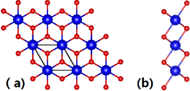
Figure 1 shows the structure of monolayer, containing three atomic sublayers with Yb layer sandwiched I layers. The similar structure can also be found in TMD monolayerq20 , such as and monolayers with 1T phase. However, it is different from the as a representative TMD monolayer with 2H phase. The unit cell of monolayer is built with the vacuum region of more than 18 to avoid spurious interaction between neighboring layers. The optimized lattice constants () using GGA is 4.46 with Yb and I atoms occupying the (0, 0, 0) and (1/3, 2/3, 0.922) positions, respectively. The Yb-I bond length is 3.14 , and I-Yb-I bond angle for (), and the thicknesses of monolayer for 3.58 .
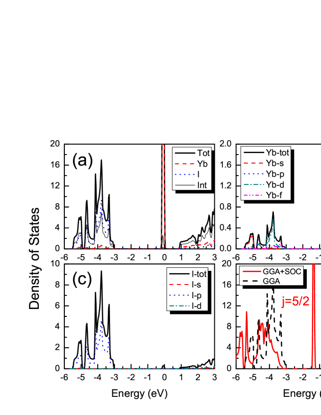
The calculated energy band structures of monolayer are shown in Figure 2 with GGA and GGA+SOC, and the related density of states (DOS) are plotted in Figure 3. Without SOC, fourteen highly localized bands with Yb- character are observed near the Fermi level, and the bandwidth is only 0.118 eV. When including SOC, the bands are split into the and states, producing a gap of 1.218 eV. Similar splitting can also be found in by SOCqsoc . The states are near the Fermi level with bandwidth 0.092 eV, and states are -1.309 eV below the Fermi level with bandwidth 0.086 eV. Both using GGA and GGA+SOC, the valence band maximum (VBM) is at point, and the conduction band minimum (CBM) at M point. The GGA and GGA+SOC gap is 0.916 eV and 0.390 eV, respectively, and the gap reduce caused by SOC is 0.526 eV. The bands from -5.5 to -3.0 eV are mainly composed of I-p character states, slightly hybridized with Yb-d/s ones. The hybridized Yb-d and I states are observed in the conduction bands. When considering SOC, it is found that both conduction bands and valence bands below localized states move toward lower energy compared with ones using GGA.
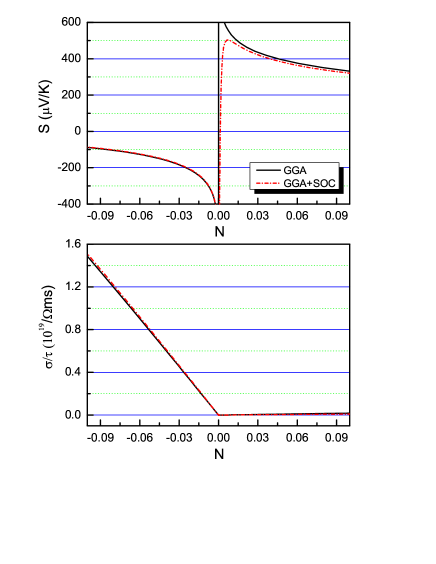
The electronic transport coefficients of TMD monolayers have been widely investigated in theoryq21 ; q22 ; q23 . It is natural to ask what effects on transport coefficients can be induced by highly localized bands. Based on CSTA Boltzmann theory, the Seebeck coefficient S and electrical conductivity are performed within rigid band approach. It is noted that the calculated depends on , while S is independent of . The n(p)-type doping effects can be simulated by simply moving the Fermi level into conduction (valence) bands, namely electron (hole) doping. The room temperature S and of as a function of doping level (N) using GGA and GGA+SOC are plotted in Figure 4. In low p-type doping, a detrimental influence on S caused by SOC can be observed, while a neglectful effect on S (absolute value) in n-type or high p-type doping can be found. For , the SOC has little effect in both n- and p-type doping. It is clearly seen that the p-type S is larger than 300 V/K with doping level being up to 0.1 hole/per unit cell. However, for n-type doping, the S can reach 300 V/K, only below doping level of 0.008 electron/per unit cell. It is also found that the is very close to zero in p-type doping. These results are because the S is proportional to the effective mass of the carrier, while is inversely proportional to one. Therefore, highly localized bands can induce very large S and very low by producing very large effective mass of the carrier. A similar effect can be found in hole-doped PbTe or PbSeq24 ; q25 , and the flat-band (localized bands) can be observed below their gaps.
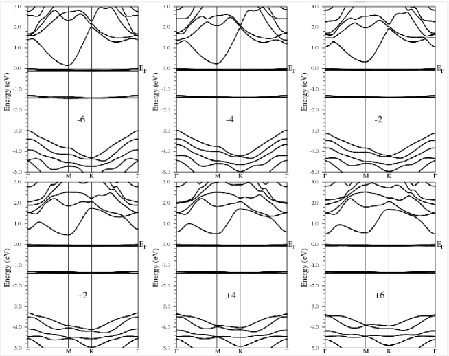
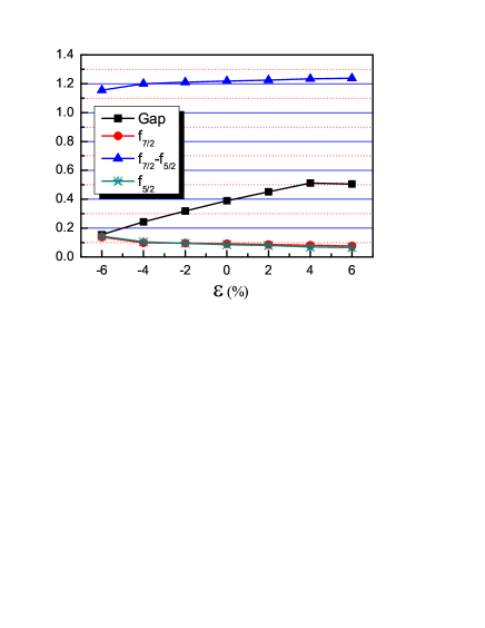
During the fabrication process, 2D materials will commonly have residual strain. Next, we investigate the stability of highly localized bands again biaxial strain. The strain effects on the energy band structures and transport properties of TMD monolayers have been widely investigatedq22 ; q23 ; q26 ; q27 . The is defined to simulate biaxial strain, in which is the unstrained lattice constant. The ()0 means compressive (tensile) strain. The related energy band structures of monolayer are shown in Figure 5 using GGA+SOC, with strain from -6% to 6%. In considered strain range, compressive strain can reduce the numbers of conduction band extrema (CBE) from two to one, while tensile strain can change relative position of two CBE. For example, at 6% strain, the CBM changes from M to point, which means that tensile strain can induce conduction bands convergence between 4% and 6% strain, producing very large n-type S. Similar phenomenon caused by strain can also be found in TMD monolayersq22 ; q23 ; q27 . The energy band gap, the gap between the and states and the widths of the and states as a function of are plotted in Figure 6. With increasing strain, the energy band gap increases from -6% to 4% strain, and then slightly reduces at 6% strain. It is clearly seen that the gap between the and states and the widths of the and states have very minor changes from -4% to 6% strain, and the change is only 0.038 eV, 0.023 eV and 0.039 eV, respectively. So, the highly localized bands have very strong stability again strain.
IV Discussions and Conclusion
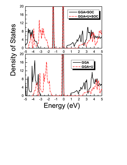
To account for electron correlation effects, the onsite Coulomb interaction is included, and the Coulomb potential for the Yb- orbitals is chosen to be 5 eV. The DOS of using GGA+SOC, GGA++SOC, GGA and GGA+ are shown in Figure 7. Calculated results show that the isolated highly localized bands still exists, and only they move to lower energies, which leads to increased energy band gap. When including onsite Coulomb interaction, the GGA gap changes from 0.92 eV to 2.53 eV, and GGA+SOC gap from 0.39 eV to 1.94 eV. However, the gap between the and states hardly changes. In fact, as is increased, highly localized bands gradually move to lower energies. When is large enough, the states firstly cross with I- states, and then the states also cross.
In summary, we investigate electronic structures of monolayer, based mainly on the reliable first-principle calculations. Calculated results show that monolayer is a indirect-gap semiconductor using GGA+SOC, GGA++SOC, GGA and GGA+, and the isolated highly localized bands with Yb- character are observed in a very large gap of up to about 4 eV. With the inclusion of SOC, the bands are split into the and states. The isolated highly localized bands can induce very large effective mass of the p-type carrier, and then leads to very large Seebeck coefficient and very low electrical conductivity in p-type doping. Calculated results show that strain can tune the strength of conduction bands convergence by changing relative position of CBE. However, the strain has little effects on isolated highly localized bands, namely they are stable again strain. The electron correlation effects only change the relative positions of highly localized bands in the gap. Our works will motivate farther experimental studies to synthesize monolayer, and then to detect isolated highly localized bands.
Acknowledgements.
This work is supported by the National Natural Science Foundation of China (Grant No. 11404391). We are grateful to the Advanced Analysis and Computation Center of CUMT for the award of CPU hours to accomplish this work.References
- (1) K. S. Novoselov et al., Science 306, 666 (2004).
- (2) R. X. Fei, W. B. Li, J. Li and L. Yang, Appl. Phys. Lett. 107, 173104 (2015).
- (3) J. P. Ji, X. F. Song, J. Z. Liu et al., Nat. Commun. 7, 13352 (2016).
- (4) S. L. Zhang M. Q. Xie, F. Y. Li, Z. Yan, Y. F. Li, E. J. Kan, W. Liu, Z. F. Chen, H. B. Zeng, Angew. Chem. 128, 1698 (2016).
- (5) S. Balendhran, S. Walia, H. Nili, S. Sriram and M.Bhaskaran, small 11, 640 (2015).
- (6) M. Chhowalla, H. S. Shin, G. Eda, L. J. Li, K. P. Loh and H. Zhang, Nature Chemistry 5, 263 (2013).
- (7) B. Radisavljevic, A. Radenovic, J. Brivio, V. Giacometti and A. Kis, Nat. Nanotechnol. 6, 147 (2011).
- (8) D. Jariwala, V. K. Sangwan, L. J. Lauhon, T. J. Marks and M. C. Hersam, ACS Nano 8, 1102 (2014).
- (9) A. Y. Lu, H. Y. Zhu, J. Xiao et al., Nature Nanotechnology 12, 744 (2017).
- (10) H. Liu, A. T. Neal, Z. Zhu, Z. Luo, X. Xu, D. Tomnek, and P. D. Ye, ACS Nano 8, 4033 (2014).
- (11) H. O. H. Churchill and P. Jarillo-Herrero, Nat. Nanotech. 9, 330 (2014).
- (12) B. J. Feng, B. T. Fu, S. Kasamatsu et al., Nat. Commun. 8, 1007 (2017).
- (13) C. Shao, X. X. Yu, N. Yang, Y. N. Yue and H. Bao, Nanosc. Microsc. Therm. 21, 201 (2017).
- (14) N. Mounet, M. Gibertini, P. Schwaller et al., Nat. Nanotechnol. 13, 246 (2018).
- (15) P. Hohenberg and W. Kohn, Phys. Rev. 136, B864 (1964); W. Kohn and L. J. Sham, Phys. Rev. 140, A1133 (1965).
- (16) P. Blaha, K. Schwarz, G. K. H. Madsen, D. Kvasnicka and J. Luitz, WIEN2k, an Augmented Plane Wave + Local Orbitals Program for Calculating Crystal Properties (Karlheinz Schwarz Technische Universität Wien, Austria) 2001, ISBN 3-9501031-1-2
- (17) J. P. Perdew, K. Burke and M. Ernzerhof, Phys. Rev. Lett. 77, 3865 (1996).
- (18) A. H. MacDonald, W. E. Pickett and D. D. Koelling, J. Phys. C 13, 2675 (1980).
- (19) D. J. Singh and L. Nordstrom, Plane Waves, Pseudopotentials and the LAPW Method, 2nd Edition (Springer, New York, 2006).
- (20) J. Kunes, P. Novak, R. Schmid, P. Blaha and K. Schwarz, Phys. Rev. B 64, 153102 (2001).
- (21) D. D. Koelling, B. N. Harmon, J. Phys. C: Solid State Phys. 10, 3107 (1977).
- (22) G. K. H. Madsen and D. J. Singh, Comput. Phys. Commun. 175, 67 (2006).
- (23) H. L. Zhuang and R. G. Hennig, J. Phys. Chem. C 117, 20440 (2013).
- (24) T. R. Chang, T. Das, P. J. Chen et al., Phys. Rev. B 91, 155151 (2015).
- (25) S. D. Guo and J. L. Wang, Semicond. Sci. Tech. 31, 095011 (2016).
- (26) H. Y. Lv, W. J. Lu, D. F. Shao, H. Y. Lub and Y. P. Sun, J. Mater. Chem. C 4, 4538 (2016).
- (27) S. D. Guo, J. Mater. Chem. C 4, 9366 (2016).
- (28) D. Parker and D. J. Singh, Phys. Rev. B 82, 035204 (2010).
- (29) D. J. Singh, Phys. Rev. B 81, 195217 (2010).
- (30) E. Scalise, M. Houssa, G. Pourtois, V. Afanas’ev and A. Stesmans, Nano Res. 5, 43 (2012).
- (31) D. Qin, X. J. Ge, G. Q. Ding, G. Y. Gao and J. T. Lv, RSC Adv. 7, 47243 (2017).