Quartz tuning-fork based carbon nanotube transfer into quantum device geometries
Abstract
With the objective of integrating single clean, as-grown carbon nanotubes into complex circuits, we have developed a technique to grow nanotubes directly on commercially available quartz tuning forks using a high temperature CVD process. Multiple straight and aligned nanotubes bridge the gap between the two tips. The nanotubes are then lowered onto contact electrodes, electronically characterized in situ, and subsequently cut loose from the tuning fork using a high current. First quantum transport measurements of the resulting devices at cryogenic temperatures display Coulomb blockade characteristics.
I Introduction
A fabrication technique that has led to many remarkable observations in quantum transport is the in-situ growth of carbon nanotubes onto pre-existing electrodes and trenches in between them Cao et al. (2005). Published results range from Coulomb blockade transport spectroscopy of unperturbed electronic systems Deshpande and Bockrath (2008); Kuemmeth et al. (2008); Pecker et al. (2013); Marganska et al. (2017) all the way to high quality factor mechanical resonators and strong interaction between single electron tunneling and vibrational motion Hüttel et al. (2009); Steele et al. (2009); Lassagne et al. (2009); Hüttel et al. (2010); Götz et al. (2018). A natural limitation of this technique is that the electrode chip is exposed to the conditions of chemical vapour deposition (CVD) nanotube growth, typically in a gas mixture of hydrogen and methane at Kong et al. (1998). Only few thin film materials survive this process, notably platinum-tungsten combinations Cao et al. (2005); Hüttel et al. (2009) and rhenium or rhenium-molybdenum alloys Singh et al. (2014); Schmid et al. (2015); Götz et al. (2016); Blien et al. (2016). Still, fabrication remains challenging and the integration of more sensitive circuit elements such as, e.g., Josephson junctions, quasi impossible.
The separation of growth and measurement chip provides a compelling alternative to in-situ growth of CNTs Wu et al. (2010); Pei et al. (2012); Ranjan et al. (2015); Waissman et al. (2013); Gramich et al. (2015). For the subsequent transfer of the nanotubes from one to the other, several approaches exist. While pressing growth surfaces directly onto the measurement chip to transfer CNTs potentially provides many viable devices per fabrication step and allows the lithographic selection of suitable CNTs on the target surface for contacting Desjardins et al. (2017); Paradiso et al. (2018), the integration of clean, suspended CNTs into complex, large-scale circuits requires a controlled deposition of single macromolecules Ranjan et al. (2015); Waissman et al. (2013); Gramich et al. (2015).
Here, we present a technique to grow clean CNTs between the two prongs of commercially available quartz tuning forks and subsequently deposit them onto contact electrodes of arbitrary material. We demonstrate the details of the substrates, the transfer, and the cutting process and show first low temperature transport data.
II CNT growth on quartz tuning forks
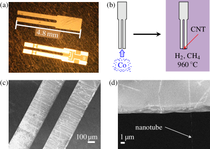
We start with a wafer piece containing several commercial-grade quartz tuning forks, see Fig. 1(a). After breaking out one or more forks, the metallic contacts are removed using aqua regia, hot hydrochloric acid and hot NaOH baths and successive cleaning steps of sonication and plasma ashing. Then, a nominally thick layer of cobalt is sputter-deposited onto the tips of a fork, see Fig. 1(b). For such a nominal thickness Co does not form a homogeneous film, but a randomly distributed ensemble of Co clusters which serve as catalyst centers for the carbon nanotube growth Kumar and Ando (2010); Yuan et al. (2008).
As next step, the forks are placed on a glass plate and inserted into the quartz tube of a CVD furnace. The furnace is heated up under a steady flow of an argon / hydrogen mixture and then kept at for 30 minutes under a constant gas flow of methane and hydrogen. The flow rates, \ceCH4 and \ceH2, are typical for clean CNT growth Kong et al. (1998). The fork is placed perpendicular to the gas stream. As a result, the growth is directional in the sense that CNTs grow mainly in the prong-to-prong direction, see Fig. 1(b) and also Fig. 1(c,d), where the entire fork surface has been covered with catalyst for better visibility of the resulting nanotube growth.
Imaging the forks in a scanning electron microscope after growth, we find that even with catalyst coating only the fork tips typically up to five nanotubes or nanotube bundles per fork are suspended over the gap between the tips Kasumov et al. (2007); Marganska et al. (2017). To avoid damage and carbon contamination, we do not image forks that are actually used for transfer. In a future setup one could imagine using optical means, as, e.g., Raman or photoluminescence imaging Lefebvre et al. (2006) to count the suspended nanotubes between the fork prongs.
III Target chip
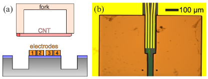
For first tests of the transfer process, devices with four long electrodes were prepared via optical lithography, see Fig. 2(a) for a schematic side view and Fig. 2(b) for a microscope top view. The substrate is highly p-doped silicon, with a thermally grown surface oxide. On its surface, four finger-like gold electrodes are deposited using thermal evaporation, and lift-off. The typical width of the electrodes and the distance between them are both for this simplified test device. Next to the electrodes, two rectangular areas are locally etched to a depth of by an anisotropic reactive ion etching process using \ceSF6 and Ar. The etch depth should be as large as possible and is mainly limited by the lithographic resist protecting the remaining structure.
IV Transfer and cutting process
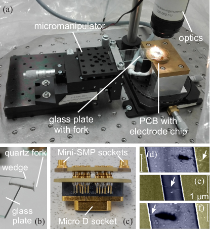
For the transfer, the quartz fork carrying as-grown CNTs is attached to a glass object plate and mounted on a micromanipulator stage, see Figs. 3(a) and (b). The setup is adapted from the equipment combination used in Castellanos-Gomez et al. (2014) to dry-stamp 2D materials. As there, a camera combined with a zoom lens allows us to observe the target chip from the top. The base plate is modified insofar as it clamps a printed circuit board sample holder with a 25-pin MDM socket at the bottom, see Fig. 3(c). The target chip is glued onto the circuit board and bonded; the electrodes are electrically contacted during the transfer process.
Using the micromanipulator stage, the quartz fork is lowered onto the chip such that its tips sink into the deep-etched areas on both sides of the dc contacts, cf. Fig. 2(a). The process is monitored both optically and electrically. On the one hand, we use the microscope camera to monitor the fork position during the alignment. On the other hand, by applying 100 mV between contacts 1 and 4, see Fig. 2(a), we can detect a CNT bridging the metal electrodes by simply measuring a finite current.
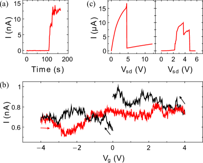
This is illustrated in Fig. 4(a), where at a time index of contact is made. Back gate voltage sweeps, see Fig. 4(b), then allow us to estimate whether a semiconducting or metallic nanotube or a nanotube bundle is contacted.
By ramping up a voltage bias and thereby the current between contacts 1 and 2, as well as subsequently between contacts 3 and 4, while the device is in air, the segments of the tube between these contacts can be electrically cut. Example current-voltage characteristics during this process are plotted in Fig. 4(c). The critical current for cutting a nanotube typically lies in the range of , consistent with the findings of Refs. Waissman et al. (2013); Gramich et al. (2015). If at a certain point the current drops to zero in one single step as, e.g., in the left part of Fig. 4(c), this indicates that one single-wall carbon nanotube has been cut. If the current decreases to zero in several steps as in the right part of Fig. 4(c) the segment was a multi-wall nanotube or bundle and the steps correspond to breaking the shells or nanotubes one at a time. We were able to verify this interpretation of the number of steps in the I-V-curves by extracting the diameter of successfully transferred nanotubes from atomic force microscopy images at large contact distances, where the nanotubes can touch the substrate.
If the approach of fork and target chip is not done carefully enough, a nanotube can be ripped off the fork tips and then fall down to the substrate in the deep-etched areas. Then, electrodes 1 and 2 are still electrically connected via the substrate even after the nanotube segment between them has been cut, resulting in a tail of finite current in the I-V-curve, cf. Fig.4(c), left panel.
V Cleaning of the quartz forks for re-use
After successful completion of the cutting process the detached nanotube lies only over the inner contact pair (2 and 3), as can be seen in the SEM image of Fig. 3(e). The quartz fork can then be safely lifted and removed.
Given the chemical and mechanical stability of the tuning forks, a rigorous cleaning procedure can subsequently be applied to remove both carbon residues and cobalt catalyst. We use plasma ashing to remove organic compounds grown in the preceding CVD process, and a bath of hot nitric acid to dissolve residues of old catalyst. After sonication and another short plasma ashing step the forks can be reintroduced into the fabrication cycle by sputtering a new layer of Co catalyst.
VI Low temperature characterization
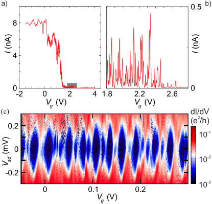
After successfully transferring a carbon nanotube to a substrate similar to the one shown in Fig. 2, we have cooled down the device to liquid helium temperature. The device was fabricated on a highly doped Si wafer, such that the substrate can be electrically connected and used as a global backgate. Fig. 5(a) shows the current through the CNT in dependence on the gate voltage , when 2 mV bias is applied. Several distinct gate voltage regions can be distinguished in the figure. For the nanotube is strongly coupled to the electrodes, resulting in an open system. In the region Coulomb blockade and single electron tunneling peaks are visible; see Fig. 5(b) for a detail zoom. For no current is flowing, indicating an electronic band gap.
A stability diagram at millikelvin temperatures of a similar device, where a carbon nanotube was deposited as described here, is shown in Fig. 5(c). The figure displays the differential conductance as function of the source-drain voltage and a gate voltage . One can clearly identify the characteristic diamond pattern of Coulomb blockade regions as typically shown by quantum dots.
The stability diagram of Fig. 5(c) indicates a predominant electrostatic charging energy of approximately , corresponding to a total quantum dot capacitance of . This is significantly larger than typical values for a device with single-wall nanotube length and a distance to the gate of , the values expected from the contact geometry here. The small charging energy may indicate that multiwall nanotubes, bundles or nanotube networks have been transferred and measured. The appearance of an additional set of smaller Coulomb blockade areas in Fig. 5(c) supports this, indicating a second confined electronic system. No transversal mechanical resonance was found in transport measurements in a frequency range of Hüttel et al. (2009). Further optimization of the CVD parameters and the transfer procedure to produce solitary single-wall carbon nanotubes is thus required.
VII Conclusions and outlook
We have implemented a technique for carbon nanotube transfer separating growth and measurement onto different substrates. Nanotubes are grown on the tips of commercially available quartz tuning forks and subsequently transferred to a target chip of desired design.
As with other nanotube transfer procedures, the choice of contact materials and circuit elements for the target chip is much less constrained than for in situ overgrowth, carbon nanotubes not suitable for measurements can easily be removed, and complex-structured devices can be re-used in more than one transfer attempt. Transfer targets may range from, e.g., superconducting coplanar circuit geometries Xiang et al. (2013); Aspelmeyer et al. (2014); Gu et al. (2017), qubit circuits Wang et al. (2017), superconducting single electron transistors Pályi et al. (2012); Struck et al. (2014), or ferromagnetic contact electrodes Stadler et al. (2015), all the way to diamond crystallites containing NV-centers Li et al. (2016).
The quartz tuning forks are standardized, macroscopic parts that can be obtained in large numbers. In addition, they are highly robust, and survive multiple cycles of catalyst deposition, growth, nanotube transfer, and cleaning. This allows an easy, systematic approach towards integrating carbon nanotubes into devices of arbitrary complexity.
Acknowledgments
The authors thank E. Weig for the initial suggestion of using quartz tuning forks, and Coftech GmbH for the quartz tuning fork wafer. Transport data has been recorded using the Lab::Measurement software package Reinhardt et al. (2018). We acknowledge funding by the Deutsche Forschungsgemeinschaft via grants Hu 1808/1, SFB 689, and GRK 1570.
References
- Cao et al. (2005) J. Cao, Q. Wang, and H. Dai, “Electron transport in very clean, as-grown suspended carbon nanotubes,” Nature Materials 4, 745–749 (2005).
- Deshpande and Bockrath (2008) V. V. Deshpande and M. Bockrath, “The one-dimensional Wigner crystal in carbon nanotubes,” Nature Physics 4, 314–318 (2008).
- Kuemmeth et al. (2008) F. Kuemmeth, S. Ilani, D. C. Ralph, and P. L. McEuen, “Coupling of spin and orbital motion of electrons in carbon nanotubes,” Nature 452, 448–452 (2008).
- Pecker et al. (2013) S. Pecker, F. Kuemmeth, A. Secchi, M. Rontani, D. C. Ralph, P.L. McEuen, and S. Ilani, “Observation and spectroscopy of a two-electron Wigner molecule in an ultraclean carbon nanotube,” Nat. Phys. 9, 576 (2013).
- Marganska et al. (2017) M. Marganska, D. R. Schmid, P. L. Stiller, A. Dirnaichner, Ch. Strunk, M. Grifoni, and A. K. Hüttel, “Shaping electron wave functions in a carbon nanotube with a parallel magnetic field,” (2017), arXiv:1712.08545.
- Hüttel et al. (2009) A. K. Hüttel, G. A. Steele, B. Witkamp, M. Poot, L. P. Kouwenhoven, and H. S. J. van der Zant, “Carbon nanotubes as ultra-high quality factor mechanical resonators,” Nano Letters 9, 2547–2552 (2009).
- Steele et al. (2009) G. A. Steele, A. K. Hüttel, B. Witkamp, M. Poot, H. B. Meerwaldt, L. P. Kouwenhoven, and H. S. J. van der Zant, “Strong coupling between single-electron tunneling and nanomechanical motion,” Science 325, 1103 (2009).
- Lassagne et al. (2009) B. Lassagne, Y. Tarakanov, J. Kinaret, D. Garcia-Sanchez, and A. Bachtold, “Coupling mechanics to charge transport in carbon nanotube mechanical resonators,” Science 28, 1107 (2009).
- Hüttel et al. (2010) A. K. Hüttel, H. B. Meerwaldt, G. A. Steele, M. Poot, B. Witkamp, L. P. Kouwenhoven, and H. S. J. van der Zant, “Single electron tunneling through high-Q single-wall carbon nanotube NEMS resonators,” phys. stat. sol. (b) 247, 2974 (2010).
- Götz et al. (2018) K. J. G. Götz, D. R. Schmid, F. J. Schupp, P. L. Stiller, Ch. Strunk, and A. K. Hüttel, “Nanomechanical characterization of the Kondo charge dynamics in a carbon nanotube,” (2018), arXiv:1802.00522.
- Kong et al. (1998) J. Kong, H. T. Soh, A. M. Cassell, C. F. Quate, and H. Dai, “Synthesis of individual single-walled carbon nanotubes on patterned silicon wafers,” Nature 395, 878 (1998).
- Singh et al. (2014) V. Singh, B. H. Schneider, S. J. Bosman, E. P. J. Merkx, and G. A. Steele, “Molybdenum-rhenium alloy based high-Q superconducting mircowave resonators,” Applied Physics Letters 105, 222601 (2014).
- Schmid et al. (2015) D. R. Schmid, S. Smirnov, M. Margańska, A. Dirnaichner, P. L. Stiller, M. Grifoni, A. K. Hüttel, and C. Strunk, “Broken SU(4) symmetry in a Kondo-correlated carbon nanotube,” Physical Review B 91, 155435 (2015).
- Götz et al. (2016) K. J. G. Götz, S. Blien, P. L. Stiller, O. Vavra, T. Mayer, T. Huber, T. N. G. Meier, M. Kronseder, Ch. Strunk, and A. K. Hüttel, Nanotechnology 27, 135202 (2016).
- Blien et al. (2016) S. Blien, K. J. G. Götz, P. L. Stiller, T. Mayer, T. Huber, O. Vavra, and A. K. Hüttel, “Towards carbon nanotube growth into superconducting microwave resonator geometries,” phys. stat. sol. (b) 253, 2385 (2016).
- Wu et al. (2010) Chung Chiang Wu, Chang Hua Liu, and Zhaohui Zhong, “One-step direct transfer of pristine single-walled carbon nanotubes for functional nanoelectronics,” Nano Letters 10, 1032–1036 (2010).
- Pei et al. (2012) Fei Pei, Edward A. Laird, Gary A. Steele, and Leo P. Kouwenhoven, “Valley-spin blockade and spin resonance in carbon nanotubes,” Nature Nanotechnology 7, 630–634 (2012).
- Ranjan et al. (2015) V. Ranjan, G. Puebla-Hellmann, M. Jung, T. Hasler, A. Nunnenkamp, M. Muoth, C. Hierold, A. Wallraff, and C. Schönenberger, “Clean carbon nanotubes coupled to superconducting impedance-matching circuits,” Nature Communications 6, 7165 (2015).
- Waissman et al. (2013) J. Waissman, M. Honig, S. Pecker, A. Benyamini, A. Hamo, and S. Ilani, “Realization of pristine and locally tunable one-dimensional electron systems in carbon nanotubes,” Nature Nanotechnology 8, 569 (2013).
- Gramich et al. (2015) Jörg Gramich, Andreas Baumgartner, Matthias Muoth, Christofer Hierold, and Christian Schönenberger, “Fork stamping of pristine carbon nanotubes onto ferromagnetic contacts for spin-valve devices,” physica status solidi (b) 252, 2496–2502 (2015).
- Desjardins et al. (2017) M. M. Desjardins, J. J. Viennot, M. C. Dartiailh, L. E. Bruhat, M. R. Delbecq, M. Lee, M.-S. Choi, A. Cottet, and T. Kontos, “Observation of the frozen charge of a Kondo resonance,” Nature 545, 4 (2017).
- Paradiso et al. (2018) N. Paradiso et al., (2018), in preparation.
- Kumar and Ando (2010) Mukul Kumar and Yoshinori Ando, “Chemical vapor deposition of carbon nanotubes: a review on growth mechanism and mass production,” Journal of Nanoscience and Nanotechnology 10, 3739–3758 (2010).
- Yuan et al. (2008) Dongning Yuan, Lei Ding, Haibin Chu, Yiyu Feng, Thomas P. McNicholas, and Jie Liu, “Horizontally aligned single-walled carbon nanotube on quartz from a large variety of metal catalysts,” Nano Letters 8, 2576–2579 (2008).
- Kasumov et al. (2007) Y. A. Kasumov, A. Shailos, I. I. Khodos, V. T. Volkov, V. I. Levashov, V. N. Matveev, S. Guéron, M. Kobylko, M. Kociak, H. Bouchiat, V. Agache, A. S. Rollier, L. Buchaillot, A. M. Bonnot, and A. Y. Kasumov, “CVD growth of carbon nanotubes at very low pressure of acetylene,” Applied Physics A 88, 687–691 (2007).
- Lefebvre et al. (2006) Jacques Lefebvre, David G. Austing, Jeffery Bond, and Paul Finnie, “Photoluminescence imaging of suspended single-walled carbon nanotubes,” Nano Letters 6, 1603–1608 (2006).
- Castellanos-Gomez et al. (2014) Andres Castellanos-Gomez, Michele Buscema, Rianda Molenaar, Vibhor Singh, Laurens Janssen, Herre S J van der Zant, and Gary A Steele, “Deterministic transfer of two-dimensional materials by all-dry viscoelastic stamping,” 2D Materials 1, 011002 (2014).
- Xiang et al. (2013) Ze-Liang Xiang, Sahel Ashhab, J. Q. You, and Franco Nori, “Hybrid quantum circuits: Superconducting circuits interacting with other quantum systems,” Rev. Mod. Phys. 85, 623–653 (2013).
- Aspelmeyer et al. (2014) Markus Aspelmeyer, Tobias J. Kippenberg, and Florian Marquardt, “Cavity optomechanics,” Rev. Mod. Phys. 86, 1391–1452 (2014).
- Gu et al. (2017) Xiu Gu, Anton Frisk Kockum, Adam Miranowicz, Yu-Xi Liu, and Franco Nori, “Microwave photonics with superconducting quantum circuits,” Physics Reports 718-719, 1 – 102 (2017).
- Wang et al. (2017) Xin Wang, Adam Miranowicz, Hong-Rong Li, and Franco Nori, “Hybrid quantum device with a carbon nanotube and a flux qubit for dissipative quantum engineering,” Phys. Rev. B 95, 205415 (2017).
- Pályi et al. (2012) András Pályi, P. R. Struck, Mark Rudner, Karsten Flensberg, and Guido Burkard, “Spin-orbit-induced strong coupling of a single spin to a nanomechanical resonator,” Phys. Rev. Lett. 108, 206811 (2012).
- Struck et al. (2014) Philipp R. Struck, Heng Wang, and Guido Burkard, “Nanomechanical readout of a single spin,” Phys. Rev. B 89, 045404 (2014).
- Stadler et al. (2015) P. Stadler, W. Belzig, and G. Rastelli, “Control of vibrational states by spin-polarized transport in a carbon nanotube resonator,” Phys. Rev. B 91, 085432 (2015).
- Li et al. (2016) Peng-Bo Li, Ze-Liang Xiang, Peter Rabl, and Franco Nori, “Hybrid quantum device with nitrogen-vacancy centers in diamond coupled to carbon nanotubes,” Phys. Rev. Lett. 117, 015502 (2016).
- Reinhardt et al. (2018) S. Reinhardt, C. Butschkow, S. Geissler, A. Dirnaichner, F. Olbrich, C. Lane, D. Schröer, and A. K. Hüttel, “Lab::Measurement — a portable and extensible framework for controlling lab equipment and conducting measurements,” arXiv preprint (2018), arXiv:1804.03321.