Techniques for Shared Resource Management
in Systems with Throughput Processors
Copyright © 2017 Rachata Ausavarungnirun
Acknowledgements
First and foremost, I would like to thank my parents, Khrieng and Ruchanee Ausavarungnirun for their endless encouragement, love, and support. In addition to my family, I would like to thank my advisor, Prof. Onur Mutlu, for providing me with great research environment. He taught me many important aspects of research and shaped me into the researcher I am today.
I would like to thank all my committee members, Prof. James Hoe, Dr. Gabriel Loh, Prof. Chris Rossbach and Prof. Kayvon Fatahalian, who provided me multiple feedback on my research and spent a lot of their time and effort to help me complete this dissertation. Special thank to Professor James Hoe, my first mentor at CMU, who taught me all the basics since my sophomore year. Professor Hoe introduced me to many interesting research projects within CALCM. Thanks to Dr. Gabriel Loh for his guidance, which helped me tremendously during the first four years of my PhD. Thanks to Prof. Chris Rossbach for being a great mentor, providing me with guidance, feedback and support for my research. Both Dr. Loh and Prof. Rossbach provided me with lots of real-world knowledge from the industry, which further enhanced the quality of my research. Lastly, thanks to Prof. Kayvon Fatahalian for his knowledge and valuable comments on my GPU research.
All members of SAFARI have been like a family to me. This dissertation is done thanks to lots of support and feedback from them. Donghyuk Lee has always been a good friend and a great mentor. His work ethic is something I always look up to. Thanks to Kevin Chang for all the valuable feedback throughout my PhD. Thanks to Yoongu Kim and Lavanya Subramanian for teaching me on several DRAM-related topics. Thanks to Samira Khan and Saugata Ghose for their guidance. Thanks to Hongyi Xin and Yixin Luo for their positive attitudes and their friendship. Thanks to Vivek Seshadri and Gennady Pekhimenko for their research insights. Thanks to Chris Fallin and Justin Meza for all the helps, especially during the early years of my PhD. They provided tremendous help when I am preparing for my qualification exam. Thanks to Nandita Vijaykumar for all GPU-related discussions. Thanks to Hanbin Yoon, Jamie Liu, Ben Jaiyen, Chris Craik, Kevin Hsieh, Yang Li, Amirali Bouroumand, Jeremie Kim, Damla Senol and Minesh Patel for all their interesting research discussions.
In additional to people in the SAFARI group, I would like to thank Onur Kayiran and Adwait Jog, who have been great colleagues and have been providing me with valuable discussions on various GPU-related research topics. Thanks to Mohammad Fattah for a great collaboration on Network-on-chip. Thanks to Prof. Reetu Das for her inputs on my Network-on-chip research projects. Thanks to Eriko Nurvitadhi and Peter Milder, both of whom were my mentors during my undergrad years. Thanks to John and Claire Bertucci for their fellowship support. Thanks to Dr. Pattana Wangaryattawanich and Dr. Polakit Teekakirikul for their friendship and mental support. Thanks to several members of the Thai Scholar community as well as several members of the Thai community in Pittsburgh for their friendship. Thanks to support from AMD, Facebook, Google, IBM, Intel, Microsoft, NVIDIA, Qualcomm, VMware, Samsung, SRC, and support from NSF grants numbers 0953246, 1065112, 1147397, 1205618, 1212962, 1213052, 1302225, 1302557, 1317560, 1320478, 1320531, 1409095, 1409723, 1423172, 1439021 and 1439057.
Lastly, I would like to give a special thank to my wife, Chatchanan Doungkamchan for her endless love, support and encouragement. She understands me and helps me with every hurdle I have been through. Her work ethic and the care she gives to her research motivate me to work harder to become a better researcher. She provides me with the perfect environment that allows me to focus on improving myself and my work while trying to make sure neither of us are burned-out from over working. I could not have completed any of the works done in this dissertation without her support.
Abstract
The continued growth of the computational capability of throughput processors has made throughput processors the platform of choice for a wide variety of high performance computing applications. Graphics Processing Units (GPUs) are a prime example of throughput processors that can deliver high performance for applications ranging from typical graphics applications to general-purpose data parallel (GPGPU) applications. However, this success has been accompanied by new performance bottlenecks throughout the memory hierarchy of GPU-based systems. This dissertation identifies and eliminates performance bottlenecks caused by major sources of interference throughout the memory hierarchy.
Specifically, we provide an in-depth analysis of inter- and intra-application as well as inter-address-space interference that significantly degrade the performance and efficiency of GPU-based systems.
To minimize such interference, we introduce changes to the memory hierarchy for systems with GPUs that allow the memory hierarchy to be aware of both CPU and GPU applications’ characteristics. We introduce mechanisms to dynamically analyze different applications’ characteristics and propose four major changes throughout the memory hierarchy.
First, we introduce Memory Divergence Correction (MeDiC), a cache management mechanism that mitigates intra-application interference in GPGPU applications by allowing the shared L2 cache and the memory controller to be aware of the GPU’s warp-level memory divergence characteristics. MeDiC uses this warp-level memory divergence information to give more cache space and more memory bandwidth to warps that benefit most from utilizing such resources. Our evaluations show that MeDiC significantly outperforms multiple state-of-the-art caching policies proposed for GPUs.
Second, we introduce the Staged Memory Scheduler (SMS), an application-aware CPU-GPU memory request scheduler that mitigates inter-application interference in heterogeneous CPU-GPU systems. SMS creates a fundamentally new approach to memory controller design that decouples the memory controller into three significantly simpler structures, each of which has a separate task, These structures operate together to greatly improve both system performance and fairness. Our three-stage memory controller first groups requests based on row-buffer locality. This grouping allows the second stage to focus on inter-application scheduling decisions. These two stages enforce high-level policies regarding performance and fairness. As a result, the last stage is simple logic that deals only with the low-level DRAM commands and timing. SMS is also configurable: it allows the system software to trade off between the quality of service provided to the CPU versus GPU applications. Our evaluations show that SMS not only reduces inter-application interference caused by the GPU, thereby improving heterogeneous system performance, but also provides better scalability and power efficiency compared to multiple state-of-the-art memory schedulers.
Third, we redesign the GPU memory management unit to efficiently handle new problems caused by the massive address translation parallelism present in GPU computation units in multi-GPU-application environments. Running multiple GPGPU applications concurrently induces significant inter-core thrashing on the shared address translation/protection units; e.g., the shared Translation Lookaside Buffer (TLB), a new phenomenon that we call inter-address-space interference. To reduce this interference, we introduce Multi Address Space Concurrent Kernels (MASK). MASK introduces TLB-awareness throughout the GPU memory hierarchy and introduces TLB- and cache-bypassing techniques to increase the effectiveness of a shared TLB.
Finally, we introduce Mosaic, a hardware-software cooperative technique that further increases the effectiveness of TLB by modifying the memory allocation policy in the system software. Mosaic introduces a high-throughput method to support large pages in multi-GPU-application environments. The key idea is to ensure memory allocation preserve address space contiguity to allow pages to be coalesced without any data movements. Our evaluations show that the MASK-Mosaic combination provides a simple mechanism that eliminates the performance overhead of address translation in GPUs without significant changes to GPU hardware, thereby greatly improving GPU system performance.
The key conclusion of this dissertation is that a combination of GPU-aware cache and memory management techniques can effectively mitigate the memory interference on current and future GPU-based systems as well as other types of throughput processors.
Chapter 1 Introduction
Throughput processor is a type of processors that consists of numerous simple processing cores. Throughput processor allows applications to achieve very high throughput by executing a massive number of compute operations on these processing cores in parallel within a single cycle [388, 370, 87, 158, 84, 369, 48, 364, 410, 411, 389, 148, 13, 26, 5, 432, 61, 179, 80, 181, 344, 278, 307, 308, 310, 311, 312, 315, 7, 8, 427]. These throughput processors incorporate a variety of processing paradigms, such as vector processors, which utilize a specific execution model called Single Instruction Multiple Data (SIMD) model that allows one instruction to be operated on multiple data [388, 370, 87, 158, 84, 369, 48, 364], processors that utilize a technique called fine-grained multithreading, which allows the processor to issue instructions from different threads after every cycle [410, 411, 389, 148, 13, 26], or processors that utilize both techniques [5, 432, 61, 179, 80, 181, 344, 278, 307, 308, 310, 311, 312, 315, 7, 8, 427]. One of the most prominent throughput processors available in modern day computing systems that utilize both SIMD execution model and fine-grained multithreading is the Graphics Processing Units (GPUs). This dissertation uses GPUs as an example class of throughput processors.
GPUs have enormous parallel processing power due to the large number of computational units they provide. Modern GPU programming models exploit this processing power using a large amount of thread-level parallelism. GPU applications can be broken down into thousands of threads, allowing GPUs to use an execution model called SIMT (Single Instruction Multiple Thread), which enables the GPU cores to tolerate dependencies and long memory latencies. The thousands of threads within a GPU application are clustered into work groups (or thread blocks), where each thread block consists of a collection of threads that are run concurrently. Within a thread block, threads are further grouped into smaller units, called warps [251] or wavefronts [11]. Every cycle, each GPU core executes a single warp. Each thread in a warp executes the same instruction (i.e., is at the same program counter) in lockstep, which is an example of the SIMD (Single Instruction, Multiple Data) [116] execution model. This highly-parallel SIMT/SIMD execution model allows the GPU to complete several hundreds to thousands of operations every cycle.
GPUs are present in many modern systems. These GPU-based systems range from traditional discrete GPUs [310, 311, 312, 315, 7, 8, 427, 278, 344] to heterogeneous CPU-GPU architectures [5, 432, 61, 179, 80, 181, 344, 278, 307, 308]. In all of these systems with GPUs, resources throughout the memory hierarchy, e.g., core-private and shared caches, main memory, the interconnects, and the memory management units are shared across multiple threads and processes that execute concurrently in both the CPUs and the GPUs.
1.1 Resource Contention and Memory Interference Problem in Systems with GPUs
Due to the limited shared resources in these systems, applications oftentimes are not able to achieve their ideal throughput (as measured by, e.g., computed instructions per cycle). Shared resources become the bottleneck and create inefficiency because accesses from one thread or application can interfere with accesses from other threads or applications in any shared resources, leading to both bandwidth and space contention, resulting in lower performance. The main goal of this dissertation is to analyze and mitigate the major memory interference problems throughout shared resources in the memory hierarchy of current and future systems with GPUs.
We focus on three major types of memory interference that occur in systems with GPUs: 1) intra-application interference among different GPU threads, 2) inter-application interference that is caused by both CPU and GPU applications, and 3) inter-address-space interference during address translation when multiple GPGPU applications concurrently share the GPUs.
Intra-application interference is a type of interference that originates from GPU threads within the same GPU application. When a GPU executes a GPGPU application, the threads that are scheduled to run on the GPU cores execute concurrently. Even though these threads belong to the same kernel, they contend for shared resources, causing interference to each other [36, 247, 78, 79]. This intra-application interference leads to the significant slowdown of threads running on GPU cores and lowers the performance of the GPU.
Inter-application interference is a type of interference that is caused by concurrently-executing CPU and GPU applications. It occurs in systems where a CPU and a GPU share the main memory system. This type of interference is especially observed in recent heterogeneous CPU-GPU systems [181, 179, 176, 178, 62, 61, 432, 307, 80, 344, 278, 33, 209, 207, 187], which introduce an integrated Graphics Processing Unit (GPU) on the same die with the CPU cores. Due to the GPU’s ability to execute a very large number of parallel threads, GPU applications typically demand significantly more memory bandwidth than typical CPU applications. Unlike GPU applications that are designed to tolerate the long memory latency by employing massive amounts of multithreading [33, 179, 181, 61, 432, 310, 311, 312, 315, 7, 8, 9, 80, 344, 278, 427, 307, 308], CPU applications typically have much lower tolerance to latency [33, 220, 221, 398, 400, 399, 402, 292, 293, 103, 234]. The high bandwidth consumption of the GPU applications heavily interferes with the progress of other CPU applications that share the same hardware resources.
Inter-address-space interference arises due to the address translation process in an environment where multiple GPU applications share the same GPU, e.g., a shared GPU in a cloud infrastructure. We discover that when multiple GPGPU applications concurrently use the same GPU, the address translation process creates additional contention at the shared memory hierarchy, including the Translation Lookaside Buffers (TLBs), caches, and main memory. This particular type of interference can cause a severe slowdown to all applications and the system when multiple GPGPU applications are concurrently executed on a system with GPUs.
While previous works propose mechanisms to reduce interference and improve the performance of GPUs (See Chapter 3 for a detailed analyses of these previous works), these approaches 1) focus only on a subset of the shared resources, such as the shared cache or the memory controller and 2) generally do not take into account the characteristics of the applications executing on the GPUs.
1.2 Thesis Statement and Our Overarching Approach:
Application Awareness
With the understanding of the causes of memory interference, our thesis statement is that a combination of GPU-aware cache and memory management techniques can mitigate memory interference caused by GPUs on current and future systems with GPUs. To this end, we propose to mitigate memory interference in current and future GPU-based systems via GPU-aware and GPU-application-aware resource management techniques. We redesign the memory hierarchy such that each component in the memory hierarchy is aware of the GPU applications’ characteristics. The key idea of our approach is to extract important features of different applications in the system and use them in managing memory hierarchy resources much more intelligently. These key features consist of, but are not limited to, memory access characteristics, utilization of the shared cache, usage of shared main memory and demand for the shared TLB. Exploiting these features, we introduce modifications to the shared cache, the memory request scheduler, the shared TLB and the GPU memory allocator to reduce the amount of inter-application, intra-application and inter-address-space interference based on applications’ characteristics. We give a brief overview of our major new mechanisms in the rest of this section.
1.2.1 Minimizing Intra-application Interference
Intra-application interference occurs when multiple threads in the GPU contend for the shared cache and the shared main memory. Memory requests from one thread can interfere with memory requests from other threads, leading to low system performance. As a step to reduce this intra-application interference, we introduce Memory Divergence Correction (MeDiC) [36], a cache and memory controller management scheme that is designed to be aware of different types of warps that access the shared cache, and selectively prioritize warps that benefit the most from utilizing the cache. This new mechanism first characterizes different types of warps based on how much benefit they receive from the shared cache. To effectively characterize warp-type, MeDiC uses the memory divergence patterns, i.e., the diversity of how long each load and store instructions in the warp takes. We observe that GPGPU applications exhibit different levels of heterogeneity in their memory divergence behavior at the shared L2 cache within the GPU. As a result, (1) some warps benefit significantly from the cache, while others make poor use of it; (2) the divergence behavior of a warp tends to remain stable for long periods of the warp’s execution; and (3) the impact of memory divergence can be amplified by the high queuing latencies at the L2 cache.
Based on the heterogeneity in warps’ memory divergence behavior, we propose a set of techniques, collectively called Memory Divergence Correction (MeDiC), that reduce the negative performance impact of memory divergence and cache queuing. MeDiC uses warp divergence characterization to guide three warp-aware components in the memory hierarchy: (1) a cache bypassing mechanism that exploits the latency tolerance of warps that do not benefit from using the cache, to both alleviate queuing delay and increase the hit rate for warps that benefit from using the cache, (2) a cache insertion policy that prevents data from warps that benefit from using the cache from being prematurely evicted, and (3) a memory controller that prioritizes the few requests received from warps that benefit from using the cache, to minimize stall time. Our evaluation shows that MeDiC is effective at exploiting inter-warp heterogeneity and delivers significant performance and energy improvements over the state-of-the-art GPU cache management technique [247].
1.2.2 Minimizing Inter-application Interference
Inter-application interference occurs when multiple processor cores (CPUs) and a GPU integrated together on the same chip share the off-chip DRAM (and perhaps some caches). In such as system, requests from the GPU can heavily interfere with requests from the CPUs, leading to low system performance and starvation of cores. Even though previously-proposed application-aware memory scheduling policies designed for CPU-only scenarios (e.g., [357, 293, 220, 221, 292, 234, 398, 400, 399, 402, 103]) can be applied on a CPU-GPU heterogeneous system, we observe that the GPU requests occupy a significant portion of request buffer space and thus reduce the visibility of CPU cores’ requests to the memory controller, leading to lower system performance. Increasing the request buffer space requires complex logic to analyze applications’ characteristics, assign priorities for each memory request and enforce these priorities when the GPU is present. As a result, these past proposals for application-aware memory scheduling in CPU-only systems can perform poorly on a CPU-GPU heterogeneous system at low complexity (as we show in this dissertation).
To minimize the inter-application interference in CPU-GPU heterogeneous systems, we introduce a new memory controller called the Staged Memory Scheduler (SMS) [33], which is both application-aware and GPU-aware. Specifically, SMS is designed to facilitate GPU applications’ high bandwidth demand, improving performance and fairness significantly. SMS introduces a fundamentally new approach that decouples the three primary tasks of the memory controller into three significantly simpler structures that together improve system performance and fairness. The three-stage memory controller first groups requests based on row-buffer locality in its first stage, called the Batch Formation stage. This grouping allows the second stage, called the Batch Scheduler stage, to focus mainly on inter-application scheduling decisions. These two stages collectively enforce high-level policies regarding performance and fairness, and therefore the last stage can get away with using simple per-bank FIFO queues (no further command reordering within each bank) and straight forward logic that deals only with the low-level DRAM commands and timing. This last stage is called the DRAM Command Scheduler stage.
Our evaluation shows that SMS is effective at reducing inter-application interference. SMS delivers superior performance and fairness compared to state-of-the-art memory schedulers [357, 293, 220, 221], while providing a design that is significantly simpler to implement and that has significantly lower power consumption.
1.2.3 Minimizing Inter-address-space Interference
Inter-address-space interference occurs when the GPU is shared among multiple GPGPU applications in large-scale computing environments [311, 310, 312, 315, 9, 31, 421, 191]. Much of the inter-address-space interference problem in a contemporary GPU lies within the memory system, where multi-application execution requires virtual memory support to manage the address spaces of each application and to provide memory protection. We observe that when multiple GPGPU applications spatially share the GPU, a significant amount of inter-core thrashing occurs on the shared TLB within the GPU. We observe that this contention at the shared TLB is high enough to prevent the GPU from successfully hiding memory latencies, which causes TLB contention to become a first-order performance concern.
Based on our analysis of the TLB contention in a modern GPU system executing multiple applications, we introduce two mechanisms. First, we design Multi Address Space Concurrent Kernels (MASK). The key idea of MASK is to 1) extend the GPU memory hierarchy to efficiently support address translation via the use of multi-level TLBs, and 2) use translation-aware memory and cache management techniques to maximize throughput in the presence of inter-address-space contention. MASK uses a novel token-based approach to reduce TLB miss overheads by limiting the number of thread that can use the shared TLB, and its L2 cache bypassing mechanisms and address-space-aware memory scheduling reduce the inter-address-space interference. We show that MASK restores much of the thread-level parallelism that was previously lost due to address translation.
Second, to further minimize the inter-address-space interference, we introduce Mosaic. Mosaic significantly decreases inter-address-space interference at the shared TLB by increasing TLB reach via support for multiple page sizes, including very large pages. To enable multi-page-size support, we provide two key observations. First, we observe that the vast majority of memory allocations and memory deallocations are performed en masse by GPGPU applications in phases, typically soon after kernel launch or before kernel exit. Second, long-lived memory objects that usually increase fragmentation and induce complexity in CPU memory management are largely absent in the GPU setting. These two observations make it relatively easy to predict memory access patterns of GPGPU applications and simplify the task of detecting when a memory region can benefit from using large pages.
Based on the prediction of the memory access patterns, Mosaic 1) modifies GPGPU applications’ memory layout in system software to preserve address space contiguity, which allows the GPU to splinter and coalesce pages very fast without moving data and 2) periodically performs memory compaction while still preserving address space contiguity to avoid memory bloat and data fragmentation. Our prototype shows that Mosaic is very effective at reducing inter-address-space interference at the shared TLB and limits the number of shared TLB miss rate to less than 1% on average (down from 25.4% in the baseline shared TLB).
In summary, MASK incorporates TLB-awareness throughout the memory hierarchy and introduces TLB- and cache-bypassing techniques to increase the effectiveness of a shared TLB. Mosaic provides a hardware-software cooperative technique that modifies the memory allocation policy in the system software and introduces a high-throughput method to support large pages in multi-GPU-application environments. The MASK-Mosaic combination provides a simple mechanism to eliminate the performance overhead of address translation in GPUs without requiring significant changes in GPU hardware. These techniques work together to significantly improve system performance, IPC throughput, and fairness over the state-of-the-art memory management technique [343].
1.3 Contributions
We make the following major contributions:
-
•
We provide an in-depth analyses of three different types of memory interference in systems with GPUs. Each of these three types of interference significantly degrades the performance and efficiency of the GPU-based systems. To minimize memory interference, we introduce mechanisms to dynamically analyze different applications’ characteristics and propose four major changes throughout the memory hierarchy of GPU-based systems.
-
•
We introduce Memory Divergence Correction (MeDiC). MeDiC is a mechanism that minimizes intra-application interference in systems with GPUs. MeDiC is the first work that observes that the different warps within a GPGPU application exhibit heterogeneity in their memory divergence behavior at the shared L2 cache, and that some warps do not benefit from the few cache hits that they have. We show that this memory divergence behavior tends to remain consistent throughout long periods of execution for a warp, allowing for fast, online warp divergence characterization and prediction. MeDiC takes advantage of this warp characterization via a combination of warp-aware cache bypassing, cache insertion and memory scheduling techniques. Chapter 4 provides the detailed design and evaluation of MeDiC.
-
•
We demonstrate how the GPU memory traffic in heterogeneous CPU-GPU systems can cause severe inter-application interference, leading to poor performance and fairness. We propose a new memory controller design, the Staged Memory Scheduler (SMS), which delivers superior performance and fairness compared to three state-of-the-art memory schedulers [357, 220, 221], while providing a design that is significantly simpler to implement. The key insight behind SMS’s scalability is that the primary functions of sophisticated memory controller algorithms can be decoupled into different stages in a multi-level scheduler. Chapter 5 provides the design and the evaluation of SMS in detail.
-
•
We perform a detailed analysis of the major problems in state-of-the-art GPU virtual memory management that hinders high-performance multi-application execution. We discover a new type of memory interference, which we call inter-address-space interference, that arises from a significant amount of inter-core thrashing on the shared TLB within the GPU. We also discover that the TLB contention is high enough to prevent the GPU from successfully hiding memory latencies, which causes TLB contention to become a first-order performance concern in GPU-based systems. Based on our analysis, we introduce Multi Address Space Concurrent Kernels (MASK). MASK extends the GPU memory hierarchy to efficiently support address translation through the use of multi-level TLBs, and uses translation-aware memory and cache management to maximize IPC (instruction per cycle) throughput in the presence of inter-application contention. MASK restores much of the thread-level parallelism that was previously lost due to address translation. Chapter 6 analyzes the effect of inter-address-space interference and provides the detailed design and evaluation of MASK.
-
•
To further minimize the inter-address-space interference, we introduce Mosaic. Mosaic further increases the effectiveness of TLB by providing a hardware-software cooperative technique that modifies the memory allocation policy in the system software. Mosaic introduces a low overhead method to support large pages in multi-GPU-application environments. The key idea of Mosaic is to ensure memory allocation preserve address space contiguity to allow pages to be coalesced without any data movements. Our prototype shows that Mosaic significantly increases the effectiveness of the shared TLB in a GPU and further reduces inter-address-space interference. Chapter 7 provides the detailed design and evaluation of Mosaic.
1.4 Dissertation Outline
This dissertation is organized into eight Chapters. Chapter 2 presents background on modern GPU-based systems. Chapter 3 discusses related prior works on resource management, where techniques can potentially be applied to reduce interference in GPU-based systems. Chapter 4 presents the design and evaluation of MeDiC. MeDiC is a mechanism that minimizes intra-application interference by redesigning the shared cache and the memory controller to be aware of different types of warps. Chapter 5 presents the design and evaluation of SMS. SMS is a GPU-aware and application-aware memory controller design that minimizes the inter-application interference. Chapter 6 presents a detailed analysis of the performance impact of inter-address-space interference. It then proposes MASK, a mechanism that minimizes inter-address-space interference by introducing TLB-awareness throughout the memory hierarchy. Chapter 7 presents the design for Mosaic. Mosaic provides a hardware-software cooperative technique that reduces inter-address-space interference by lowering contention at the shared TLB. Chapter 8 provides the summary of common principles and lessons learned. Chapter 9 provides the summary of this dissertation as well as future research directions that are enabled by this dissertation.
Chapter 2 The Memory Interference Problem in Systems with GPUs
We first provide background on the architecture of a modern GPU, and then we discuss the bottlenecks that highly-multithreaded applications can face either when executed alone on a GPU or when executing with other CPU or GPU applications.
2.1 Modern Systems with GPUs
In this section, we provide a detailed explanation of the GPU architecture that is available on modern systems. Section 2.1 discusses a typical modern GPU architecture [310, 311, 312, 315, 7, 8, 427, 278, 344, 5, 432, 61, 179, 80, 181, 307, 308] as well as its memory hierarchy. Section 2.2 discusses the design of a modern CPU-GPU heterogeneous architecture [432, 61, 179, 181] and its memory hierarchy. Section 2.3 discusses the memory management unit and support for address translation.
2.1.1 GPU Core Organization
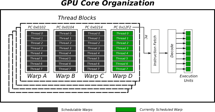
A typical GPU consists of several GPU cores called shader cores (sometimes called streaming multiprocessors, or SMs). As shown in Figure 2.1, a GPU core executes SIMD-like instructions [116]. Each SIMD instruction can potentially operate on multiple pieces of data in parallel. Each data piece operated on by a different thread of control. Hence, the name SIMT (Single Instruction Multiple Thread). Multiple threads that are the same are grouped into a warp. A warp is a collection of threads that are executing the same instruction (i.e., are at the same Program Counter). Multiple warps are grouped into a thread block. Every cycle, a GPU core fetches an available warp (a warp is available if none of its threads are stalled), and issues an instruction associated with those threads (in the example from Figure 2.1, this instruction is from Warp D and the address of this instruction is ). In this way, a GPU can potentially retire as many instructions as the number of cores multiplied by the number of threads per warp, enabling high instruction-per-cycle (IPC) throughput. More detail on GPU core organization can be found in [121, 129, 271, 120, 46, 436, 150, 385].
2.1.2 GPU Memory Hierarchy
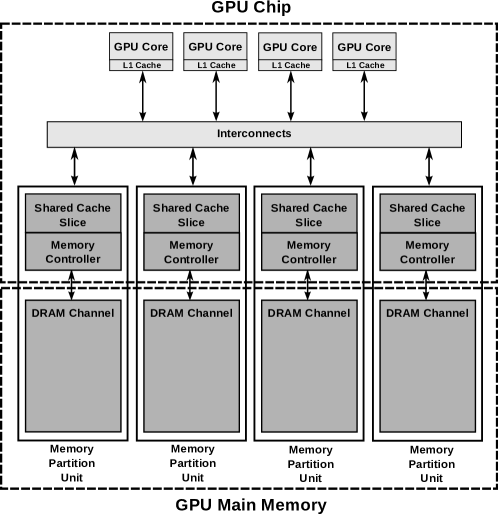
When there is a load or store instruction that needs to access data from the main memory, the GPU core sends a memory request to the memory hierarchy, which is shown in Figure 2.2. This hierarchy typically contains a private data cache, and an interconnect (typically a crossbar) that connects all the cores with the shared data cache. If the target data is present neither in the private nor the shared data cache, a memory request is sent to the main memory in order to retrieve the data.
GPU Cache Organization and Key Assumptions. Each core has its own private L1 data, texture, and constant caches, as well as a software-managed scratchpad memory [311, 310, 251, 312, 315, 8, 11, 423]. In addition, the GPU also has several shared L2 cache slices and memory controllers. Because there are several methods to design the GPU memory hierarchy, we assume the baseline that decouples the memory channels into multiple memory partitions. A memory partition unit combines a single L2 cache slice (which is banked) with a designated memory controller that connects the GPU to off-chip main memory. Figure 2.2 shows a simplified view of how the cores (or SMs), caches, and memory partitions are organized in our baseline GPU.
GPU Main Memory Organization. Similar to systems with CPUs, a GPU uses DRAM (organized as hierarchical two-dimensional arrays of bitcells) as main memory. Reading or writing data to DRAM requires that a row of bitcells from the array first be read into a row buffer. This is required because the act of reading the row destroys the row’s contents, and so a copy of the bit values must be kept (in the row buffer). Reads and writes operate directly on the row buffer. Eventually, the row is “closed” whereby the data in the row buffer is written back into the DRAM array. Accessing data already loaded in the row buffer, also called a row buffer hit, incurs a shorter latency than when the corresponding row must first be “opened” from the DRAM array. A modern memory controller (memory controller) must orchestrate the sequence of commands to open, read, write and close rows. Servicing requests in an order that increases row-buffer hit rate tends to improve overall throughput by reducing the average latency to service requests. The memory controller is also responsible for enforcing a wide variety of timing constraints imposed by modern DRAM standards (e.g., DDR3) such as limiting the rate of page-open operations (t) and ensuring a minimum amount of time between writes and reads (t). More detail on timing constraints and DRAM operation can be found in [222, 240, 241, 239, 254, 374, 71, 238, 70, 154, 155].
Each two-dimensional array of DRAM cells constitutes a bank, and a group of banks forms a rank. All banks within a rank share a common set of command and data buses, and the memory controller is responsible for scheduling commands such that each bus is used by only one bank at a time. Operations on multiple banks may occur in parallel (e.g., opening a row in one bank while reading data from another bank’s row buffer) so long as the buses are properly scheduled and any other DRAM timing constraints are honored. A memory controller can improve memory system throughput by scheduling requests such that bank-level parallelism or BLP (i.e., the number of banks simultaneously busy responding to commands) is higher [293, 237]. A memory system implementation may support multiple independent memory channels (each with its own ranks and banks) [287, 42] to further increase the number of memory requests that can be serviced at the same time. A key challenge in the implementation of modern, high-performance memory controllers is to effectively improve system performance by maximizing both row-buffer hits and BLP while simultaneously providing fairness among multiple CPUs and the GPU [33].
2.1.3 Intra-application Interference within GPU Applications
While many GPGPU applications can tolerate a significant amount of memory latency due to their parallelism through the SIMT execution model, many previous works (e.g., [425, 193, 297, 192, 46, 436, 150, 120, 121, 74, 359, 360, 271]) observe that GPU cores often stall for a significant fraction of time. One significant source of these stalls is the contention at the shared GPU memory hierarchy [297, 271, 359, 425, 193, 192, 207, 74, 36]. The large amount of parallelism in GPU-based systems creates a significant amount of contention on the GPU’s memory hierarchy. Even through all threads in the GPU execute the codes from the same application, data accesses from one warp can interfere with data accesses from other warps. This interference comes in several forms such as additional cache thrashing and queuing delays at both the shared cache and shared main memory. These combine to lower the performance of GPU-based systems. We call this interference the intra-application interference.
Memory divergence, where the threads of a warp reach a memory instruction, and some of the threads’ memory requests take longer to service than the requests from other threads [297, 271, 74, 36], further exacerbates the effect of intra-application interference. Since all threads within a warp operate in lockstep due to the SIMD execution model, the warp cannot proceed to the next instruction until the slowest request within the warp completes, and all threads are ready to continue execution.
Chapter 4 provides detailed analyses on how to reduce intra-application interference at the shared cache and the shared main memory.
2.2 GPUs in CPU-GPU Heterogeneous Architectures
Aside from using off-chip discrete GPUs, modern architectures integrate Graphics Processors integrate a GPU on the same chip as the CPU cores [181, 179, 176, 178, 62, 61, 432, 307, 80, 344, 278, 33, 209, 187]. Figure 2.3 shows the design of these recent heterogeneous CPU-GPU architecture. As shown in Figure 2.3, parts of the memory hierarchy are being shared across both CPU and GPU applications.
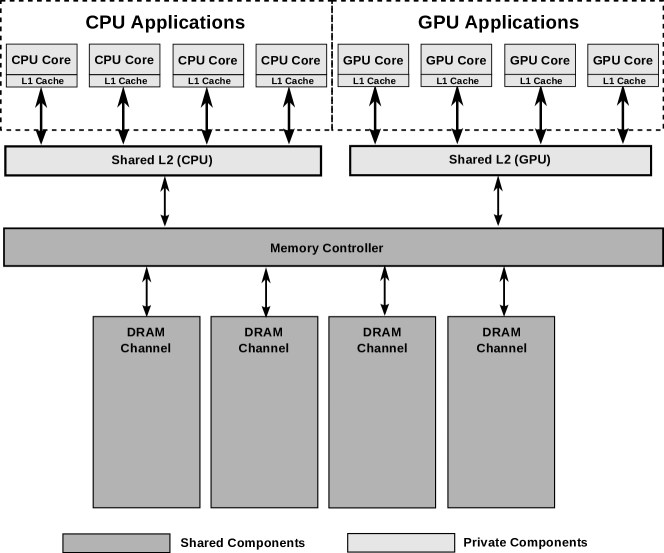
Key Assumptions. We make two key assumptions for the design of heterogeneous CPU-GPU systems. First, we assume that the GPUs and the CPUs do not share the last level caches. Second, we assume that the memory controller is the first point in the memory hierarchy that CPU applications and GPU applications share resources. We applied multiple memory scheduler designs as the baseline for our evaluations. Additional details of these baseline design can be found in Sections 5.3.5 and 5.4.
2.2.1 Inter-application Interference across CPU and GPU Applications
As illustrated in Figure 2.3, the main memory is a major shared resource among cores in modern chip multiprocessor (CMP) systems. Memory requests from multiple cores interfere with each other at the main memory and create inter-application interference, which is a significant impediment to individual application and system performance. Previous works on CPU-only application-aware memory scheduling [292, 293, 220, 221, 398, 103, 234] have addressed the problem by being aware of application characteristics at the memory controller and prioritizing memory requests to improve system performance and fairness. This approach of application-aware memory request scheduling has provided good system performance and fairness in multicore systems.
As opposed to CPU applications, GPU applications are not very latency sensitive as there are a large number of independent threads to cover long memory latencies. However, the GPU requires a significant amount of bandwidth far exceeding even the most memory-intensive CPU applications. As a result, a GPU memory scheduler [251, 311, 315] typically needs a large request buffer that is capable of request coalescing (i.e., combining multiple requests for the same block of memory into a single combined request [251]). Furthermore, since GPU applications are bandwidth intensive, often with streaming access patterns, a policy that maximizes the number of row-buffer hits is effective for GPUs to maximize overall throughput. Hence, a memory scheduler that can improve the effective DRAM bandwidth such as the FR-FCFS scheduler with a large request buffer [357, 454, 46, 445] tends to perform well for GPUs.
This conflicting preference between CPU applications and GPU applications (CPU applications benefit from lower memory request latency while GPU applications benefit from higher DRAM bandwidth) further complicates the design of memory request scheduler for CPU-GPU heterogeneous systems. A design that favors lowering the latency of CPU requests is undesirable for GPU applications while a design that favors providing high bandwidth is undesirable for CPU applications.
In this dissertation, Chapter 5 provides an in-depth analysis of this inter-application interference and provides a method to mitigate the interference in CPU-GPU heterogeneous architecture.
2.3 GPUs in Multi-GPU-application Environments
Recently, a newer set of analytic GPGPU applications, such as the Netflix movie recommendation systems [25], or a stock market analyzer [345], require a closely connected, highly virtualized, shared environment. These applications, which benefit from the amount of parallelism GPU provides, do not need to use all resources in the GPU to maximize their performance. Instead, these emerging applications benefit from concurrency - by running a few of these applications together, each sharing some resources on the GPU. NVIDIA GRID [311, 315] and AMD FirePro [9] are two examples of spatially share GPU resources across multiple applications.
Figure 2.4 shows the high-level design of how a GPU can be spatially shared across two GPGPU applications. In this example, the GPUs contain multiple shared page table walkers, which are responsible for translating a virtual address into a physical address. This design also contains two level of translation lookaside buffers (TLBs), which cache the virtual-to-physical translation. This design allows the GPU to co-schedule kernels, even applications, concurrently because address translation enables memory protection across multiple GPGPU applications.

Key Assumptions. The page table walker can be placed at different locations in the GPU memory hierarchy. The GPU MMU design proposed by Power et al. places a parallel page table walkers between the private L1 and the shared L2 caches [343]. Other alternative designs place the page table walker at the Input-Output Memory Management Unit (IOMMU), which directly connects to the main memory [5, 432, 61, 179, 80, 181, 344, 278, 307, 308, 310, 311, 312, 315, 7, 8, 427, 344], and another GPU MMU design proposed by Cong et al. uses the CPU’s page table walker to perform GPU page walks [83]. We found that placing a parallel page table walkers at the shared L2 cache provides the best performance. Hence, we assume the baseline proposed by Power et al. that utilized the per-core private TLB and place the page table walker at the shared L2 cache [343].
2.3.1 Inter-address-space Interference on Multiple GPU Applications
While concurrently executing multiple GPGPU applications that have complementary resource demand can improve GPU utilization, these applications also share two critical resources: the shared address translation unit and the shared TLB. We find that when multiple applications spatially share the GPU, there is a significant amount of thrashing on the shared TLB within the GPU because multiple applications from different address spaces are contending at the shared TLB, the page table walker as well as the shared L2 data cache. We define this phenomenon as the inter-address-space interference.
The amount of parallelism on GPUs further exacerbate the performance impact of inter-address-space interference. We found that an address translation in response to a single TLB miss typically stalls tens of warps. As a result, a small number of outstanding TLB misses can result in a significant number of warps to become unschedulable, which in turn limits the GPU’s most essential latency-hiding capability. We observe that providing address translation in GPUs reduce the GPU performance to 47.3% of the ideal GPU with no address translation, which is a significant performance overhead. As a result, it is even more crucial to mitigate this inter-address-space interference throughout the GPU memory hierarchy in multi-GPU-application environments. Chapters 6 and 7 provide detailed design descriptions of the two mechanisms we propose that can be used to reduce this inter-address-space interference.
Chapter 3 Related Works on Resource Management in Systems with GPUs
Several previous works have been proposed to address the memory interference problem in systems with GPUs. These previous proposals address certain parts of the main memory hierarchy. In this chapter, we first provide the background on the GPU’s execution model. Then, we provide breakdowns of previous works on GPU resource management throughout the memory hierarchy as well as differences between these previous works and techniques presented in this dissertation.
3.1 Background on the Execution Model of GPUs
Modern day GPUs employ two main techniques to enable their parallel processing power: SIMD, which executes multiple data within a single instruction, and fine-grain multithreading, which prevents the GPU cores from stalling by issuing instructions from different threads every cycle. This section provides the background on previous machines and processors that apply similar techniques.
3.1.1 SIMD and Vector Processing
The SIMD execution model, which includes vector processing, been used by several machines in the past. Slotnik et al. in the Solomon Computer [388], Senzig and Smith [370], Crane and Guthens [87], Hellerman [158], CDC 7600 [84], CDC STAR-100 [369], Illiac IV [48] and Cray I [364] are examples of machines that employ a vector processor. In modern systems, Intel MMX [177, 336] and Intel SSE [179] also apply SIMD in order to improve performance. As an alternative of using one instruction to execute multiple data, VLIW [115] generate codes for a parallel machine that allows multiple instructions to operate on multiple data concurrently in a single cycle. Intel i860 [137] and Intel Itanium [268] are examples of processors with the VLIW technology.
3.1.2 Fine-grained Multithreading
Fine-grain multithreading, which is a technique that allows the processor to issue instructions from different threads every cycle, is the key component that enables latency hiding capability in modern day GPUs. CDC 6600 [410, 411], Denelcor HEP [389], MASA [148], APRIL [13] and Tera MTA [26] are examples of machines that utilize fine-grain multithreading.
3.2 Background on Techniques to Reduce Interference of Shared Resources
Several techniques to reduce interference at the shared cache, shared off-chip main memory as well as the shared interconnect have been proposed. In this section, we provide a brief discussion of these works.
3.2.1 Cache Bypassing Techniques
Hardware-based Cache Bypassing Techniques. Several hardware-based cache bypassing mechanisms have been proposed in both CPU and GPU setups. Li et al. propose PCAL, a bypassing mechanism that addresses the cache thrashing problem by throttling the number of threads that time-share the cache at any given time [247]. The key idea of PCAL is to limit the number of threads that get to access the cache. Li et al. [246] propose a cache bypassing mechanism that allows only threads with high reuse to utilize the cache. The key idea is to use locality filtering based on the reuse characteristics of GPGPU applications, with only high reuse threads having access to the cache. Xie et al. [439] propose a bypassing mechanism at the thread block level. In their mechanism, the compiler statically marks whether thread blocks prefer caching or bypassing. At runtime, the mechanism dynamically selects a subset of thread blocks to use the cache, to increase cache utilization. Chen et al. [78, 79] propose a combined warp throttling and bypassing mechanism for the L1 cache based on the cache-conscious warp scheduler [359]. The key idea is to bypass the cache when resource contention is detected. This is done by embedding history information into the L2 tag arrays. The L1 cache uses this information to perform bypassing decisions, and only warps with high reuse are allowed to access the L1 cache. Jia et al. propose an L1 bypassing mechanism [188], whose key idea is to bypass requests when there is an associativity stall. Dai et al. propose a mechanism to bypass cache based on a model of a cache miss rate [89].
There are also several other CPU-based cache bypassing techniques. These techniques include using additional buffers track cache statistics to predict cache blocks that have high utility based on reuse count [195, 127, 446, 215, 106, 76, 435, 252], reuse distance [99, 146, 76, 114, 326, 443, 124, 434], behavior of the cache block [185] or miss rate [82, 414]
Software-based Cache Bypassing Techniques. Because GPUs allow software to specify whether to utilize the cache or not [316, 317]. Software based cache bypassing techniques have also been proposed to improve system performance. Li et al. [245] propose a compiler-based technique that performs cache bypassing using a method similar to PCAL [247]. Xie et al. [438] propose a mechanism that allows the compiler to perform cache bypassing for global load instructions. Both of these mechanisms apply bypassing to all loads and stores that utilize the shared cache, without requiring additional characterization at the compiler level. Mekkat et al. [270] propose a bypassing mechanism for when a CPU and a GPU share the last level cache. Their key idea is to bypass GPU cache accesses when CPU applications are cache sensitive, which is not applicable to GPU-only execution.
3.2.2 Cache Insertion and Replacement Policies
Many works have proposed different insertion policies for CPU systems (e.g., [347, 379, 183, 184]). Dynamic Insertion Policy (DIP) [183] and Dynamic Re-Reference Interval Prediction (DRRIP) [184] are insertion policies that account for cache thrashing. The downside of these two policies is that they are unable to distinguish between high-reuse and low-reuse blocks in the same thread [379]. The Bi-modal Insertion Policy [347] dynamically characterizes the cache blocks being inserted. None of these works on cache insertion and replacement policies [347, 379, 183, 184] take warp type characteristics or memory divergence behavior into account.
3.2.3 Cache and Memory Partitioning Techniques
Instead of mitigating the interference problem between applications by scheduling requests at the memory controller, Awasthi et al. propose a mechanism that spreads data in the same working set across memory channels in order to increase memory level parallelism [42]. Muralidhara et al. propose memory channel partitioning (MCP) to map applications to different memory channels based on their memory-intensities and row-buffer locality to reduce inter-application interference [287]. Mao et al. propose to partition GPU channels and only allow a subset of threads to access each memory channel [266]. In addition to channel partitioning, several works also propose to partition DRAM banks [437, 171, 255] and the shared cache [401, 350] to improve performance. These partitioning techniques are orthogonal to our proposals and can be combined to improve the performance of GPU-based systems.
3.2.4 Memory Scheduling on CPUs
Memory scheduling algorithms improve system performance by reordering memory requests to deal with the different constraints and behaviors of DRAM. The first-ready-first-come-first-serve (FR-FCFS) [357] algorithm attempts to schedule requests that result in row-buffer hits (first-ready), and otherwise prioritizes older requests (FCFS). FR-FCFS increases DRAM throughput, but it can cause fairness problems by under-servicing applications with low row-buffer locality. Ebrahimi et al. [103] propose PAM, a memory scheduler that prioritizes critical threads in order to improve the performance of multithreaded applications. Ipek et al. propose a self-optimizing memory scheduling that improve system performance with reinforcement learning [405]. Mukundan and Martinez propose MORSE, a self-optimizing reconfigurable memory scheduler [285]. Lee et al. propose two prefetch aware memory scheduling designs [234, 237]. Stuecheli et al. [397] and Lee et al. [236] propose memory schedulers that are aware of writeback requests. Seshadri et al. [372] propose to simplify the implementation of row-locality-aware write back by exploiting the dirty-block index. Several application-aware memory scheduling algorithms [282, 220, 221, 292, 293, 398, 402] have been proposed to balance both performance and fairness. Parallelism-aware Batch Scheduling (PAR-BS) [293] batches requests based on their arrival times (older requests batched first). Within a batch, applications are ranked to preserve bank-level parallelism (BLP) within an application’s requests. Kim et al. propose ATLAS [220], which prioritizes applications that have received the least memory service. As a result, applications with low memory intensities, which typically attain low memory service, are prioritized. However, applications with high memory intensities are deprioritized and hence slowed down significantly, resulting in unfairness. Kim et al. further propose TCM [221], which addresses the unfairness problem in ATLAS. TCM first clusters applications into low and high memory-intensity clusters based on their memory intensities. TCM always prioritizes applications in the low memory-intensity cluster, however, among the high memory-intensity applications it shuffles request priorities to prevent unfairness. Ghose et al. propose a memory scheduler that takes into account of the criticality of each load and prioritizes loads that are more critical to CPU performance [131]. Subramanian et al. propose MISE [402], which is a memory scheduler that estimates slowdowns of applications and prioritizes applications that are likely to be slow down the most. Subramanian et al. also propose BLISS [398, 400], which is a mechanism that separates applications into a group that interferes with other applications and another group that does not, and prioritizes the latter group to increase performance and fairness. Xiong et al. propose DMPS, a ranking based on latency sensitivity [440]. Liu et al. propose LAMS, a memory scheduler that prioritizes requests based on the latency of servicing each memory request [256].
3.2.5 Memory Scheduling on GPUs
Since GPU applications are bandwidth intensive, often with streaming access patterns, a policy that maximizes the number of row-buffer hits is effective for GPUs to maximize overall throughput. As a result, FR-FCFS with a large request buffer tends to perform well for GPUs [46]. In view of this, previous work [445] designed mechanisms to reduce the complexity of row-hit first based (FR-FCFS) scheduling. Jeong et al. propose a QoS-aware memory scheduler that guarantees the performance of GPU applications by prioritizing Graphics applications over CPU applications until the system can guarantee a frame can be rendered within its deadline, and prioritize CPU applications afterward [187]. Jog et al. [194] propose CLAM, a memory scheduler that identifies critical memory requests and prioritizes them in the main memory.
Aside from CPU-GPU heterogeneous systems, Usui et at. propose SQUASH [416] and DASH [417], which are accelerator-aware memory controller designs that improve the performance of systems with CPU and hardware accelerators. Zhao et al. propose FIRM, a memory controller design that improves the performance of systems with persistent memory [450].
3.2.6 DRAM Designs
Aside from memory scheduling and memory partitioning techniques, previous works propose new designs that are capable of reducing memory latency in conventional DRAM [69, 71, 70, 240, 241, 239, 238, 222, 242, 276, 367, 151, 160, 165, 210, 391, 262, 75, 338, 382, 67, 320, 452, 431, 22, 21, 72, 289, 295] as well as non-volatile memory [275, 227, 273, 442, 351, 348, 231, 233, 232, 274]. Previous works on bulk data transfer [143, 144, 198, 65, 448, 371, 172, 451, 189, 374, 260, 71] and in-memory computation [17, 20, 112, 125, 145, 329, 373, 265, 95, 377, 375, 164, 163, 60, 395, 119, 132, 200, 224, 322, 404, 447, 23, 218, 130, 59, 43, 126, 346, 330, 376] can be used improve DRAM bandwidth. Techniques to reduce the overhead of DRAM refresh [254, 419, 53, 250, 16, 296, 253, 211, 212, 213, 214, 327, 349, 217, 44, 15, 321, 349] can be applied to improve the performance of GPU-based systems. Data compression techniques can also be used on the main memory to increase the effective DRAM bandwidth [335, 334, 332, 333, 425]. These techniques can be used to mitigate the performance impact of memory interference and improve the performance of GPU-based systems. They are orthogonal and can be combined with techniques proposed in this dissertation.
3.2.7 Interconnect Contention Management
Aside from the shared cache and the shared off-chip main memory, on-chip interconnect is another shared resources on the GPU memory hierarchy. While this dissertation does not focus on the contention of shared on-chip interconnect, many previous works provide mechanisms to reduce contention of the shared on-chip interconnect. These include works on hierarchical on-chip network designs [34, 35, 353, 449, 149, 354, 138, 92, 147, 98], low cost router designs [219, 34, 35, 286, 2, 223, 139], bufferless interconnect designs [47, 133, 156, 225, 283, 109, 68, 110, 111, 318, 319, 389, 26, 161] and Quality-of-Service-aware interconnect designs [142, 141, 140, 93, 94, 113, 91, 279].
3.3 Background on Memory Management Unit and Address Translation Designs
Aside from the caches and the main memory, the memory management unit (MMU) is another important component in the memory hierarchy. The MMU provides address translation for applications running on the GPU. When multiple GPGPU applications are concurrently running, the MMU is also provides memory protection across different virtual address spaces that are concurrently using the GPU memory. This section first introduces previous works on concurrent GPGPU application. Then, we provide background on previous works on TLB designs that aids address translation.
3.3.1 Background on Concurrent Execution of GPGPU Applications
Concurrent Kernels and GPU Multiprogramming. The opportunity to improve utilization with concurrency is well-recognized but previous proposals [323, 430, 248], do not support memory protection. Adriaens et al. [4] observe the need for spatial sharing across protection domains but do not propose or evaluate a design. NVIDIA GRID [159] and AMD FirePro [9] support static partitioning of hardware to allow kernels from different VMs to run concurrently—partitions are determined at startup, causing fragmentation and under-utilization. The goal of our proposal, MASK, is a flexible dynamic partitioning of shared resources. NVIDIA’s Multi Process Service (MPS) [314] allows multiple processes to launch kernels on the GPU: the service provides no memory protection or error containment. Xu et al [441] propose Warped-Slicer, which is a mechanism for multiple applications to spatially share a GPU core. Similar to MPS, Warped-Slicer provides no memory protection, and is not suitable for supporting multi-application in a multi-tenant cloud setting.
Preemption and Context Switching. Preemptive context switching is an active research area [409, 129, 430]. Current architectural support [251, 315] will likely improve in future GPUs. Preemption and spatial multiplexing are complementary to the goal of this dissertation, and exploring techniques to combine them is future work.
GPU Virtualization. Most current hypervisor-based full virtualization techniques for GPGPUs [206, 406, 413] must support a virtual device abstraction without dedicated hardware support for VDI found in GRID [159] and FirePro [9] . Key components missing from these proposals includes support for dynamic partitioning of hardware resources and efficient techniques for handling over-subscription. Performance overheads incurred by some of these designs argue strongly for hardware assists such as those we propose. By contrast, API-remoting solutions such as vmCUDA [429] and rCUDA [97] provide near native performance but require modifications to guest software and sacrifice both isolation and compatibility.
Other Methods to Enable Virtual Memory. Vesely et al. analyze support for virtual memory in heterogeneous systems [420], finding that the cost of address translation in GPUs is an order of magnitude higher than in CPUs and that high latency address translations limit the GPU’s latency hiding capability and hurts performance (an observation in-line with our own findings. We show additionally that thrashing due to interference further slows applications sharing the GPU. Our proposal, MASK, is capable not only of reducing interference between multiple applications, but of reducing the TLB miss rate in single-application scenarios as well. We expect that our techniques are applicable to CPU-GPU heterogeneous system.
Direct segments [51] and redundant memory mappings [201] reduce address translation overheads by mapping large contiguous virtual memory to contiguous physical address space which reduces address translation overheads by increasing the reach of TLB entries. These techniques are complementary to those in MASK, and may eventually become relevant in GPU settings as well.
Demand Paging in GPUs. Demand paging is an important functionality for memory virtualization that is challenging for GPUs [420]. Recent works [453], AMD’s hUMA [12], as well as NVIDIA’s PASCAL architecture [453, 315] support for demand paging in GPUs. As identified in MOSAIC, these techniques can be costly in GPU environment.
3.3.2 TLB Designs
GPU TLB Designs. Previous works have explored the design space for TLBs in heterogeneous systems with GPUs [83, 343, 342, 420], and the adaptation of x86-like TLBs to a heterogeneous CPU-GPU setting [343]. Key elements in these designs include probing the TLB after L1 coalescing to reduce the number of parallel TLB requests, shared concurrent page table walks, and translation caches to reduce main memory accesses. Our proposal, MASK, owes much to these designs, but we show empirically that contention patterns at the shared L2 layer require additional support to accommodate cross-context contention. Cong et al. propose a TLB design similar to our baseline GPU-MMU design [83]. However, this design utilizes the host (CPU) MMU to perform page walks, which is inapplicable in the context of multi-application GPUs. Pichai et al. [342] explore TLB design for heterogeneous CPU-GPU systems, and add TLB awareness to the existing CCWS GPU warp scheduler [359], which enables parallel TLB access on the L1 cache level, similar in concept to the Powers design [343]. Warp scheduling is orthogonal to our work: incorporating a TLB-aware CCWS warp scheduler to MASK could further improve performance.
CPU TLB Designs. Bhattacharjee et al. examine shared last-level TLB designs [57] as well as page walk cache designs [54], proposing a mechanism that can accelerate multithreaded applications by sharing translations between cores. However, these proposals are likely to be less effective for multiple concurrent GPGPU applications because translations are not shared between virtual address spaces. Barr et al. propose SpecTLB [50], which speculatively predicts address translations to avoid the TLB miss latency. Speculatively predicting address translation can be complicated and costly in GPU because there can be multiple concurrent TLB misses to many different TLB entries in the GPU.
Mechanisms to Support Multiple Page Sizes. TLB miss overheads can be reduced by accelerating page table walks [49, 54] or reducing their frequency [122]; by reducing the number of TLB misses (e.g. through prefetching [56, 199, 368], prediction [325], or structural change to the TLB [408, 340, 339] or TLB hierarchy [55, 263, 393, 19, 18, 201, 51, 123]). Multipage mapping techniques [408, 340, 339] map multiple pages with a single TLB entry, improving TLB reach by a small factor (e.g., to 8 or 16); much greater improvements to TLB reach are needed to deal with modern memory sizes. Direct segments [51, 123] extend standard paging with a large segment to map the majority of an address space to a contiguous physical memory region, but require application modifications and are limited to workloads able to a single large segment. Redundant memory mappings (RMM) [201] extend TLB reach by mapping ranges of virtually and physically contiguous pages in a range TLB.
A number of related works propose hardware support to recover and expose address space contiguity. GLUE [341] groups contiguous, aligned small page translations under a single speculative large page translation in the TLB. Speculative translations (similar to SpecTLB [50]) can be verified by off-critical-path page table walks, reducing effective page-table walk latency. GTSM [96] provides hardware support to leverage the address space contiguity of physical memory even when pages have been retired due to bit errors. Were such features to become available, hardware mechanisms for preserving address space contiguity could reduce the overheads induced by proactive compaction, which is a feature we introduce in our proposal, Mosaic.
The policies and mechanisms used to implement transparent large page support in Mosaic are informed by a wealth of previous research on operating system support for large pages for CPUs. Navarro et al. [298] identify contiguity-awareness and fragmentation reduction as primary concerns for large page management, proposing reservation-based allocation and deferred promotion of base pages to large pages. These ideas are widely used in modern operating systems [412]. Ingens [228] eschews reservation-based allocation in favor of the utilization-based promotion based on a bit vector which tracks spatial and temporal utilization of base pages, implementing promotion and demotion asynchronously, rather than in a page fault handler. These basic ideas heavily inform Mosaic’s design, which attempts to emulate these same policies in hardware. In contrast to Ingens, Mosaic can rely on dedicated hardware to provide access frequency and distribution, and need not infer it by sampling access bits whose granularity may be a poor fit for the page size.
Gorman et al. [134] propose a placement policy for an operating system’s physical page allocator that mitigates fragmentation and promotes address space contiguity by grouping pages according to relocatability. Subsequent work [135] proposes a software-exposed interface for applications to explicitly request large pages like libhugetlbfs [249]. These ideas are complementary to ideas presented in this thesis. Mosaic can plausibly benefit from similar policies simplified to be hardware-implementable, and we leave that investigation as future work.
Chapter 4 Reducing Intra-application Interference with Memory Divergence Correction
Graphics Processing Units (GPUs) have enormous parallel processing power to leverage thread-level parallelism. GPU applications can be broken down into thousands of threads, allowing GPUs to use fine-grained multithreading [410, 390] to prevent GPU cores from stalling due to dependencies and long memory latencies. Ideally, there should always be available threads for GPU cores to continue execution, preventing stalls within the core. GPUs also take advantage of the SIMD (Single Instruction, Multiple Data) execution model [116]. The thousands of threads within a GPU application are clustered into work groups (or thread blocks), with each thread block consisting of multiple smaller bundles of threads that are run concurrently. Each such thread bundle is called a wavefront [11] or warp [251]. In each cycle, each GPU core executes a single warp. Each thread in a warp executes the same instruction (i.e., is at the same program counter). Combining SIMD execution with fine-grained multithreading allows a GPU to complete several hundreds of operations every cycle in the ideal case.
In the past, GPUs strictly executed graphics applications, which naturally exhibit large amounts of concurrency. In recent years, with tools such as CUDA [313] and OpenCL [216], programmers have been able to adapt non-graphics applications to GPUs, writing these applications to have thousands of threads that can be run on a SIMD computation engine. Such adapted non-graphics programs are known as general-purpose GPU (GPGPU) applications. Prior work has demonstrated that many scientific and data analysis applications can be executed significantly faster when programmed to run on GPUs [77, 396, 157, 63].
While many GPGPU applications can tolerate a significant amount of memory latency due to their parallelism and the use of fine-grained multithreading, many previous works (e.g., [425, 193, 297, 192]) observe that GPU cores still stall for a significant fraction of time when running many other GPGPU applications. One significant source of these stalls is memory divergence, where the threads of a warp reach a memory instruction, and some of the threads’ memory requests take longer to service than the requests from other threads [297, 271, 74]. Since all threads within a warp operate in lockstep due to the SIMD execution model, the warp cannot proceed to the next instruction until the slowest request within the warp completes, and all threads are ready to continue execution. Figures 4.1a and 4.1b show examples of memory divergence within a warp, which we will explain in more detail soon.
In this work, we make three new key observations about the memory divergence behavior of GPGPU warps:
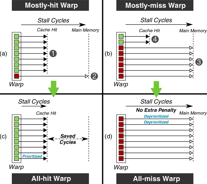
Observation 1: There is heterogeneity across warps in the degree of memory divergence experienced by each warp at the shared L2 cache (i.e., the percentage of threads within a warp that miss in the cache varies widely). Figure 4.1 shows examples of two different types of warps, with eight threads each, that exhibit different degrees of memory divergence:
-
•
Figure 4.1a shows a mostly-hit warp, where most of the warp’s memory accesses hit in the cache ( ). However, a single access misses in the cache and must go to main memory ( ). As a result, the entire warp is stalled until the much longer cache miss completes.
-
•
Figure 4.1b shows a mostly-miss warp, where most of the warp’s memory requests miss in the cache ( ), resulting in many accesses to main memory. Even though some requests are cache hits ( ), these do not benefit the execution time of the warp.
Observation 2: A warp tends to retain its memory divergence behavior (e.g., whether or not it is mostly-hit or mostly-miss) for long periods of execution, and is thus predictable. As we show in Section 4.3, this predictability enables us to perform history-based warp divergence characterization.
Observation 3: Due to the amount of thread parallelism within a GPU, a large number of memory requests can arrive at the L2 cache in a small window of execution time, leading to significant queuing delays. Prior work observes high access latencies for the shared L2 cache within a GPU [386, 385, 433], but does not identify why these latencies are so high. We show that when a large number of requests arrive at the L2 cache, both the limited number of read/write ports and backpressure from cache bank conflicts force many of these requests to queue up for long periods of time. We observe that this queuing latency can sometimes add hundreds of cycles to the cache access latency, and that non-uniform queuing across the different cache banks exacerbates memory divergence.
Based on these three observations, we aim to devise a mechanism that has two major goals: (1) convert mostly-hit warps into all-hit warps (warps where all requests hit in the cache, as shown in Figure 4.1c), and (2) convert mostly-miss warps into all-miss warps (warps where none of the requests hit in the cache, as shown in Figure 4.1d). As we can see in Figure 4.1a, the stall time due to memory divergence for the mostly-hit warp can be eliminated by converting only the single cache miss ( ) into a hit. Doing so requires additional cache space. If we convert the two cache hits of the mostly-miss warp (Figure 4.1b, ) into cache misses, we can cede the cache space previously used by these hits to the mostly-hit warp, thus converting the mostly-hit warp into an all-hit warp. Though the mostly-miss warp is now an all-miss warp (Figure 4.1d), it incurs no extra stall penalty, as the warp was already waiting on the other six cache misses to complete. Additionally, now that it is an all-miss warp, we predict that its future memory requests will also not be in the L2 cache, so we can simply have these requests bypass the cache. In doing so, the requests from the all-miss warp can completely avoid unnecessary L2 access and queuing delays. This decreases the total number of requests going to the L2 cache, thus reducing the queuing latencies for requests from mostly-hit and all-hit warps, as there is less contention.
We introduce Memory Divergence Correction (MeDiC), a GPU-specific mechanism that exploits memory divergence heterogeneity across warps at the shared cache and at main memory to improve the overall performance of GPGPU applications. MeDiC consists of three different components, which work together to achieve our goals of converting mostly-hit warps into all-hit warps and mostly-miss warps into all-miss warps: (1) a warp-type-aware cache bypassing mechanism, which prevents requests from mostly-miss and all-miss warps from accessing the shared L2 cache (Section 4.3.2); (2) a warp-type-aware cache insertion policy, which prioritizes requests from mostly-hit and all-hit warps to ensure that they all become cache hits (Section 4.3.3); and (3) a warp-type-aware memory scheduling mechanism, which prioritizes requests from mostly-hit warps that were not successfully converted to all-hit warps, in order to minimize the stall time due to divergence (Section 4.3.4). These three components are all driven by an online mechanism that can identify the expected memory divergence behavior of each warp (Section 4.3.1).
This dissertation makes the following contributions:
-
•
We observe that the different warps within a GPGPU application exhibit heterogeneity in their memory divergence behavior at the shared L2 cache, and that some warps do not benefit from the few cache hits that they have. This memory divergence behavior tends to remain consistent throughout long periods of execution for a warp, allowing for fast, online warp divergence characterization and prediction.
-
•
We identify a new performance bottleneck in GPGPU application execution that can contribute significantly to memory divergence: due to the very large number of memory requests issued by warps in GPGPU applications that contend at the shared L2 cache, many of these requests experience high cache queuing latencies.
-
•
Based on our observations, we propose Memory Divergence Correction, a new mechanism that exploits the stable memory divergence behavior of warps to (1) improve the effectiveness of the cache by favoring warps that take the most advantage of the cache, (2) address the cache queuing problem, and (3) improve the effectiveness of the memory scheduler by favoring warps that benefit most from prioritization. We compare MeDiC to four different cache management mechanisms, and show that it improves performance by 21.8% and energy efficiency by 20.1% across a wide variety of GPGPU workloads compared to a a state-of-the-art GPU cache management mechanism [247].
4.1 Background
We first provide background on the architecture of a modern GPU, and then we discuss the bottlenecks that highly-multithreaded applications can face when executed on a GPU. These applications can be compiled using OpenCL [216] or CUDA [313], either of which converts a general purpose application into a GPGPU program that can execute on a GPU.
4.1.1 Baseline GPU Architecture
A typical GPU consists of several shader cores (sometimes called streaming multiprocessors, or SMs). In this work, we set the number of shader cores to 15, with 32 threads per warp in each core, corresponding to the NVIDIA GTX480 GPU based on the Fermi architecture [310]. The GPU we evaluate can issue up to 480 concurrent memory accesses per cycle [415]. Each core has its own private L1 data, texture, and constant caches, as well as a scratchpad memory [311, 310, 251]. In addition, the GPU also has several shared L2 cache slices and memory controllers. A memory partition unit combines a single L2 cache slice (which is banked) with a designated memory controller that connects to off-chip main memory. Figure 4.2 shows a simplified view of how the cores (or SMs), caches, and memory partitions are organized in our baseline GPU.

4.1.2 Bottlenecks in GPGPU Applications
Several previous works have analyzed the benefits and limitations of using a GPU for general purpose workloads (other than graphics purposes), including characterizing the impact of microarchitectural changes on applications [46] or developing performance models that break down performance bottlenecks in GPGPU applications [243, 383, 162, 257, 264, 136]. All of these works show benefits from using a throughput-oriented GPU. However, a significant number of applications are unable to fully utilize all of the available parallelism within the GPU, leading to periods of execution where no warps are available for execution [425].
When there are no available warps, the GPU cores stall, and the application stops making progress until a warp becomes available. Prior work has investigated two problems that can delay some warps from becoming available for execution: (1) branch divergence, which occurs when a branch in the same SIMD instruction resolves into multiple different paths [46, 436, 150, 120, 297], and (2) memory divergence, which occurs when the simultaneous memory requests from a single warp spend different amounts of time retrieving their associated data from memory [297, 271, 74]. In this work, we focus on the memory divergence problem; prior work on branch divergence is complementary to our work.
4.2 Motivation and Key Observations
We make three new key observations about memory divergence (at the shared L2 cache). First, we observe that the degree of memory divergence can differ across warps. This inter-warp heterogeneity affects how well each warp takes advantage of the shared cache. Second, we observe that a warp’s memory divergence behavior tends to remain stable for long periods of execution, making it predictable. Third, we observe that requests to the shared cache experience long queuing delays due to the large amount of parallelism in GPGPU programs, which exacerbates the memory divergence problem and slows down GPU execution. Next, we describe each of these observations in detail and motivate our solutions.
4.2.1 Exploiting Heterogeneity Across Warps
We observe that different warps have different amounts of sensitivity to memory latency and cache utilization. We study the cache utilization of a warp by determining its hit ratio, the percentage of memory requests that hit in the cache when the warp issues a single memory instruction. As Figure 4.3 shows, the warps from each of our three representative GPGPU applications are distributed across all possible ranges of hit ratio, exhibiting significant heterogeneity. To better characterize warp behavior, we break the warps down into the five types shown in Figure 4.4 based on their hit ratios: all-hit, mostly-hit, balanced, mostly-miss, and all-miss.

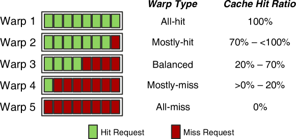
This inter-warp heterogeneity in cache utilization provides new opportunities for performance improvement. We illustrate two such opportunities by walking through a simplified example, shown in Figure 4.5. Here, we have two warps, A and B, where A is a mostly-miss warp (with three of its four memory requests being L2 cache misses) and B is a mostly-hit warp with only a single L2 cache miss (request B0). Let us assume that warp A is scheduled first.
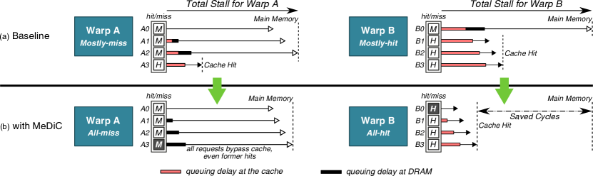
As we can see in Figure 4.5a, the mostly-miss warp A does not benefit at all from the cache: even though one of its requests (A3) hits in the cache, warp A cannot continue executing until all of its memory requests are serviced. As the figure shows, using the cache to speed up only request A3 has no material impact on warp A’s stall time. In addition, while requests A1 and A2 do not hit in the cache, they still incur a queuing latency at the cache while they wait to be looked up in the cache tag array.
On the other hand, the mostly-hit warp B can be penalized significantly. First, since warp B is scheduled after the mostly-miss warp A, all four of warp B’s requests incur a large L2 queuing delay, even though the cache was not useful to speed up warp A. On top of this unproductive delay, since request B0 misses in the cache, it holds up execution of the entire warp while it gets serviced by main memory. The overall effect is that despite having many more cache hits (and thus much better cache utility) than warp A, warp B ends up stalling for as long as or even longer than the mostly-miss warp A stalled for.
To remedy this problem, we set two goals (Figure 4.5b):
1) Convert the mostly-hit warp B into an all-hit warp. By converting B0 into a hit, warp B no longer has to stall on any memory misses, which enables the warp to become ready to execute much earlier. This requires a little additional space in the cache to store the data for B0.
2) Convert the mostly-miss warp A into an all-miss warp. Since a single cache hit is of no effect to warp A’s execution, we convert A0 into a cache miss. This frees up the cache space A0 was using, and thus creates cache space for storing B0. In addition, warp A’s requests can now skip accessing the cache and go straight to main memory, which has two benefits: A0–A2 complete faster because they no longer experience the cache queuing delay that they incurred in Figure 4.5a, and B0–B3 also complete faster because they must queue behind a smaller number of cache requests. Thus, bypassing the cache for warp A’s request allows both warps to stall for less time, improving GPU core utilization.
To realize these benefits, we propose to (1) develop a mechanism that can identify mostly-hit and mostly-miss warps; (2) design a mechanism that allows mostly-miss warps to yield their ineffective cache space to mostly-hit warps, similar to how the mostly-miss warp A in Figure 4.5a turns into an all-miss warp in Figure 4.5b, so that warps such as the mostly-hit warp B can become all-hit warps; (3) design a mechanism that bypasses the cache for requests from mostly-miss and all-miss warps such as warp A, to decrease warp stall time and reduce lengthy cache queuing latencies; and (4) prioritize requests from mostly-hit warps across the memory hierarchy, at both the shared L2 cache and at the memory controller, to minimize their stall time as much as possible, similar to how the mostly-hit warp B in Figure 4.5a turns into an all-hit warp in Figure 4.5b.
A key challenge is how to group warps into different warp types. In this work, we observe that warps tend to exhibit stable cache hit behavior over long periods of execution. A warp consists of several threads that repeatedly loop over the same instruction sequences. This secs/medic/results in similar hit/miss behavior at the cache level across different instances of the same warp. As a result, a warp measured to have a particular hit ratio is likely to maintain a similar hit ratio throughout a lengthy phase of execution. We observe that most CUDA applications exhibit this trend.
Figure 4.6 shows the hit ratio over a duration of one million cycles, for six randomly selected warps from our CUDA applications. We also plot horizontal lines to illustrate the hit ratio cutoffs that we set in Figure 4.4 for our mostly-hit (70%) and mostly-miss (20%) warp types. Warps 1, 3, and 6 spend the majority of their time with high hit ratios, and are classified as mostly-hit warps. Warps 1 and 3 do, however, exhibit some long-term (i.e., 100k+ cycles) shifts to the balanced warp type. Warps 2 and 5 spend a long time as mostly-miss warps, though they both experience a single long-term shift into balanced warp behavior. As we can see, warps tend to remain in the same warp type at least for hundreds of thousands of cycles.

As a result of this relatively stable behavior, our mechanism, MeDiC (described in detail in Section 4.3), samples the hit ratio of each warp and uses this data for warp characterization. To account for the long-term hit ratio shifts, MeDiC resamples the hit ratio every 100k cycles.
4.2.2 Reducing the Effects of L2 Queuing Latency
Unlike CPU applications, GPGPU applications can issue as many as hundreds of memory instructions per cycle. All of these memory requests can arrive concurrently at the L2 cache, which is the first shared level of the memory hierarchy, creating a bottleneck. Previous works [46, 386, 433, 385] point out that the latency for accessing the L2 cache can take hundreds of cycles, even though the nominal cache lookup latency is significantly lower (only tens of cycles). While they identify this disparity, these earlier efforts do not identify or analyze the source of these long delays.
We make a new observation that identifies an important source of the long L2 cache access delays in GPGPU systems. L2 bank conflicts can cause queuing delay, which can differ from one bank to another and lead to the disparity of cache access latencies across different banks. As Figure 4.7a shows, even if every cache access within a warp hits in the L2 cache, each access can incur a different cache latency due to non-uniform queuing, and the warp has to stall until the slowest cache access retrieves its data (i.e., memory divergence can occur). For each set of simultaneous requests issued by an all-hit warp, we define its inter-bank divergence penalty to be the difference between the fastest cache hit and the slowest cache hit, as depicted in Figure 4.7a.

In order to confirm this behavior, we modify GPGPU-Sim [46] to accurately model L2 bank conflicts and queuing delays (see Section 4.4 for details). We then measure the average and maximum inter-bank divergence penalty observed only for all-hit warps in our different CUDA applications, shown in Figure 4.7b. We find that on average, an all-hit warp has to stall for an additional 24.0 cycles because some of its requests go to cache banks with high access contention.
To quantify the magnitude of queue contention, we analyze the queuing delays for a two-bank L2 cache where the tag lookup latency is set to one cycle. We find that even with such a small cache lookup latency, a significant number of requests experience tens, if not hundreds, of cycles of queuing delay. Figure 4.8 shows the distribution of these delays for BFS [63], across all of its individual L2 cache requests. BFS contains one compute-intensive kernel and two memory-intensive kernels. We observe that requests generated by the compute-intensive kernel do not incur high queuing latencies, while requests from the memory-intensive kernels suffer from significant queuing delays. On average, across all three kernels, cache requests spend 34.8 cycles in the queue waiting to be serviced, which is quite high considering the idealized one-cycle cache lookup latency.

One naive solution to the L2 cache queuing problem is to increase the number of banks, without reducing the number of physical ports per bank and without increasing the size of the shared cache. However, as shown in Figure 4.9, the average performance improvement from doubling the number of banks to 24 (i.e., 4 banks per memory partition) is less than 4%, while the improvement from quadrupling the banks is less than 6%. There are two key reasons for this minimal performance gain. First, while more cache banks can help to distribute the queued requests, these extra banks do not change the memory divergence behavior of the warp (i.e., the warp hit ratios remain unchanged). Second, non-uniform bank access patterns still remain, causing cache requests to queue up unevenly at a few banks.111Similar problems have been observed for bank conflicts in main memory [352, 222].
4.2.3 Our Goal
Our goal of MeDiC is to improve cache utilization and reduce cache queuing latency by taking advantage of heterogeneity between different types of warps. To this end, we create a mechanism that (1) tries to eliminate mostly-hit and mostly-miss warps by converting as many of them as possible to all-hit and all-miss warps, respectively; (2) reduces the queuing delay at the L2 cache by bypassing requests from mostly-miss and all-miss warps, such that each L2 cache hit experiences a much lower overall L2 cache latency; and (3) prioritizes mostly-hit warps in the memory scheduler to minimize the amount of time they stall due to a cache miss.
4.3 MeDiC: Memory Divergence Correction
In this section, we introduce Memory Divergence Correction (MeDiC), a set of techniques that take advantage of the memory divergence heterogeneity across warps, as discussed in Section 4.2. These techniques work independently of each other, but act synergistically to provide a substantial performance improvement. In Section 4.3.1, we propose a mechanism that identifies and groups warps into different warp types based on their degree of memory divergence, as shown in Figure 4.4.
As depicted in Figure 4.10, MeDiC uses warp type identification to drive three different components: a warp-type-aware cache bypass mechanism (Section 4.3.2), which bypasses requests from all-miss and mostly-miss warps to reduce the L2 queuing delay; a warp-type-aware cache insertion policy (Section 4.3.3), which works to keep cache lines from mostly-hit warps while demoting lines from mostly-miss warps; and a warp-type-aware memory scheduler (Section 4.3.4), which prioritizes DRAM requests from mostly-hit warps as they are highly latency sensitive. We analyze the hardware cost of MeDiC in Section 4.5.5.
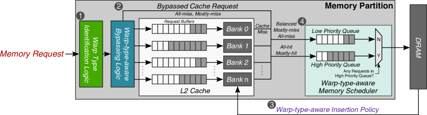
4.3.1 Warp Type Identification
In order to take advantage of the memory divergence heterogeneity across warps, we must first add hardware that can identify the divergence behavior of each warp. The key idea is to periodically sample the hit ratio of a warp, and to classify the warp’s divergence behavior as one of the five types in Figure 4.4 based on the observed hit ratio (see Section 4.2.1). This information can then be used to drive the warp-type-aware components of MeDiC. In general, warps tend to retain the same memory divergence behavior for long periods of execution. However, as we observed in Section 4.2.1, there can be some long-term shifts in warp divergence behavior, requiring periodic resampling of the hit ratio to potentially adjust the warp type.
Warp type identification through hit ratio sampling requires hardware within the cache to periodically count the number of hits and misses each warp incurs. We append two counters to the metadata stored for each warp, which represent the total number of cache hits and cache accesses for the warp. We reset these counters periodically, and set the bypass logic to operate in a profiling phase for each warp after this reset.222In this work, we reset the hit ratio every 100k cycles for each warp. During profiling, which lasts for the first 30 cache accesses of each warp, the bypass logic (which we explain in Section 4.3.2) does not make any cache bypassing decisions, to allow the counters to accurately characterize the current memory divergence behavior of the warp. At the end of profiling, the warp type is determined and stored in the metadata.
4.3.2 Warp-type-aware Shared Cache Bypassing
Once the warp type is known and a warp generates a request to the L2 cache, our mechanism first decides whether to bypass the cache based on the warp type. The key idea behind warp-type-aware cache bypassing, as discussed in Section 4.2.1, is to convert mostly-miss warps into all-miss warps, as they do not benefit greatly from the few cache hits that they get. By bypassing these requests, we achieve three benefits: (1) bypassed requests can avoid L2 queuing latencies entirely, (2) other requests that do hit in the L2 cache experience shorter queuing delays due to the reduced contention, and (3) space is created in the L2 cache for mostly-hit warps.
The cache bypassing logic must make a simple decision: if an incoming memory request was generated by a mostly-miss or all-miss warp, the request is bypassed directly to DRAM. This is determined by reading the warp type stored in the warp metadata from the warp type identification mechanism. A simple 2-bit demultiplexer can be used to determine whether a request is sent to the L2 bank arbiter, or directly to the DRAM request queue.
Dynamically Tuning the Cache Bypassing Rate. While cache bypassing alleviates queuing pressure at the L2 cache banks, it can have a negative impact on other portions of the memory partition. For example, bypassed requests that were originally cache hits now consume extra off-chip memory bandwidth, and can increase queuing delays at the DRAM queue. If we lower the number of bypassed requests (i.e., reduce the number of warps classified as mostly-miss), we can reduce DRAM utilization. After examining a random selection of kernels from three applications (BFS, BP, and CONS), we find that the ideal number of warps classified as mostly-miss differs for each kernel. Therefore, we add a mechanism that dynamically tunes the hit ratio boundary between mostly-miss warps and balanced warps (nominally set at 20%; see Figure 4.4). If the cache miss rate increases significantly, the hit ratio boundary is lowered.333In our evaluation, we reduce the threshold value between mostly-miss warps and balanced warps by 5% for every 5% increase in cache miss rate.
Cache Write Policy. Recent GPUs support multiple options for the L2 cache write policy [310]. In this work, we assume that the L2 cache is write-through [385], so our bypassing logic can always assume that DRAM contains an up-to-date copy of the data. For write-back caches, previously-proposed mechanisms [146, 384, 270] can be used in conjunction with our bypassing technique to ensure that bypassed requests get the correct data. For correctness, fences and atomic instructions from bypassed warps still access the L2 for cache lookup, but are not allowed to store data in the cache.
4.3.3 Warp-type-aware Cache Insertion Policy
Our cache bypassing mechanism frees up space within the L2 cache, which we want to use for the cache misses from mostly-hit warps (to convert these memory requests into cache hits). However, even with the new bypassing mechanism, other warps (e.g., balanced, mostly-miss) still insert some data into the cache. In order to aid the conversion of mostly-hit warps into all-hit warps, we develop a warp-type-aware cache insertion policy, whose key idea is to ensure that for a given cache set, data from mostly-miss warps are evicted first, while data from mostly-hit warps and all-hit warps are evicted last.
To ensure that a cache block from a mostly-hit warp stays in the cache for as long as possible, we insert the block closer to the MRU position. A cache block requested by a mostly-miss warp is inserted closer to the LRU position, making it more likely to be evicted. To track the status of these cache blocks, we add two bits of metadata to each cache block, indicating the warp type.444Note that cache blocks from the all-miss category share the same 2-bit value as the mostly-miss category because they always get bypassed (see Section 4.3.2). These bits are then appended to the replacement policy bits. As a result, a cache block from a mostly-miss warp is more likely to get evicted than a block from a balanced warp. Similarly, a cache block from a balanced warp is more likely to be evicted than a block from a mostly-hit or all-hit warp.
4.3.4 Warp-type-aware Memory Scheduler
Our cache bypassing mechanism and cache insertion policy work to increase the likelihood that all requests from a mostly-hit warp become cache hits, converting the warp into an all-hit warp. However, due to cache conflicts, or due to poor locality, there may still be cases when a mostly-hit warp cannot be fully converted into an all-hit warp, and is therefore unable to avoid stalling due to memory divergence as at least one of its requests has to go to DRAM. In such a case, we want to minimize the amount of time that this warp stalls. To this end, we propose a warp-type-aware memory scheduler that prioritizes the occasional DRAM request from a mostly-hit warp.
The design of our memory scheduler is very simple. Each memory request is tagged with a single bit, which is set if the memory request comes from a mostly-hit warp (or an all-hit warp, in case the warp was mischaracterized). We modify the request queue at the memory controller to contain two different queues ( in Figure 4.10), where a high-priority queue contains all requests that have their mostly-hit bit set to one. The low-priority queue contains all other requests, whose mostly-hit bits are set to zero. Each queue uses FR-FCFS [357, 454] as the scheduling policy; however, the scheduler always selects requests from the high priority queue over requests in the low priority queue.555Using two queues ensures that high-priority requests are not blocked by low-priority requests even when the low-priority queue is full. Two-queue priority also uses simpler logic design than comparator-based priority [398, 399].
4.4 Methodology
We model our mechanism using GPGPU-Sim 3.2.1 [46]. Table 7.1 shows the configuration of the GPU. We modified GPGPU-Sim to accurately model cache bank conflicts, and added the cache bypassing, cache insertion, and memory scheduling mechanisms needed to support MeDiC. We use GPUWattch [244] to evaluate power consumption.
| System Overview | 15 cores, 6 memory partitions |
|---|---|
| Shader Core Config. | 1400 MHz, 9-stage pipeline, GTO scheduler [359] |
| Private L1 Cache | 16KB, 4-way associative, LRU, L1 misses are coalesced before |
| ccessing L2, 1 cycle latency | |
| Shared L2 Cache | 768KB total, 16-way associative, LRU, 2 cache banks |
| 2 interconnect ports per memory partition, 10 cycle latency | |
| DRAM | GDDR5 1674 MHz, 6 channels (one per memory partition) |
| FR-FCFS scheduler [357, 454] 8 banks per rank, burst length 8 |
| # | Application | AH | MH | BL | MM | AM |
|---|---|---|---|---|---|---|
| 1 | Nearest Neighbor (NN) [309] | 19% | 79% | 1% | 0.9% | 0.1% |
| 2 | Convolution Separable (CONS) [309] | 9% | 1% | 82% | 1% | 7% |
| 3 | Scalar Product (SCP) [309] | 0.1% | 0.1% | 0.1% | 0.7% | 99% |
| 4 | Back Propagation (BP) [77] | 10% | 27% | 48% | 6% | 9% |
| 5 | Hotspot (HS) [77] | 1% | 29% | 69% | 0.5% | 0.5% |
| 6 | Streamcluster (SC) [77] | 6% | 0.2% | 0.5% | 0.3% | 93% |
| 7 | Inverted Index (IIX) [157] | 71% | 5% | 8% | 1% | 15% |
| 8 | Page View Count (PVC) [157] | 4% | 1% | 42% | 20% | 33% |
| 9 | Page View Rank (PVR) [157] | 18% | 3% | 28% | 4% | 47% |
| 10 | Similarity Score (SS) [157] | 67% | 1% | 11% | 1% | 20% |
| 11 | Breadth-First Search (BFS) [63] | 40% | 1% | 20% | 13% | 26% |
| 12 | Barnes-Hut N-body Simulation (BH) [63] | 84% | 0% | 0% | 1% | 15% |
| 13 | Delaunay Mesh Refinement (DMR) [63] | 81% | 3% | 3% | 1% | 12% |
| 14 | Minimum Spanning Tree (MST) [63] | 53% | 12% | 18% | 2% | 15% |
| 15 | Survey Propagation (SP) [63] | 41% | 1% | 20% | 14% | 24% |
Modeling L2 Bank Conflicts. In order to analyze the detailed caching behavior of applications in modern GPGPU architectures, we modified GPGPU-Sim to accurately model banked caches.666We validate that the performance values reported for our applications before and after our modifications to GPGPU-Sim are equivalent. Within each memory partition, we divide the shared L2 cache into two banks. When a memory request misses in the L1 cache, it is sent to the memory partition through the shared interconnect. However, it can only be sent if there is a free port available at the memory partition (we dual-port each memory partition). Once a request arrives at the port, a unified bank arbiter dispatches the request to the request queue for the appropriate cache bank (which is determined statically using some of the memory address bits). If the bank request queue is full, the request remains at the incoming port until the queue is freed up. Traveling through the port and arbiter consumes an extra cycle per request. In order to prevent a bias towards any one port or any one cache bank, the simulator rotates which port and which bank are first examined every cycle.
When a request misses in the L2 cache, it is sent to the DRAM request queue, which is shared across all L2 banks as previously implemented in GPGPU-Sim. When a request returns from DRAM, it is inserted into one of the per-bank DRAM-to-L2 queues. Requests returning from the L2 cache to the L1 cache go through a unified memory-partition-to-interconnect queue (where round-robin priority is used to insert requests from different banks into the queue).
GPGPU Applications. We evaluate our system across multiple GPGPU applications from the CUDA SDK [309], Rodinia [77], MARS [157], and Lonestar [63] benchmark suites.777We use default tuning parameters for all applications. These applications are listed in Table 4.2, along with the breakdown of warp characterization. The dominant warp type for each application is marked in bold (AH: all-hit, MH: mostly-hit, BL: balanced, MM: mostly-miss, AM: all-miss; see Figure 4.4). We simulate 500 million instructions for each kernel of our application, though some kernels complete before reaching this instruction count.
Comparisons. In addition to the baseline secs/medic/results, we compare each individual component of MeDiC with state-of-the-art policies. We compare our bypassing mechanism with three different cache management policies. First, we compare to PCAL [247], a token-based cache management mechanism. PCAL limits the number of threads that get to access the cache by using tokens. If a cache request is a miss, it causes a replacement only if the warp has a token. PCAL, as modeled in this work, first grants tokens to the warp that recently used the cache, then grants any remaining tokens to warps that access the cache in order of their arrival. Unlike the original proposal [247], which applies PCAL to the L1 caches, we apply PCAL to the shared L2 cache. We sweep the number of tokens per epoch and use the configuration that gives the best average performance. Second, we compare MeDiC against a random bypassing policy (Rand), where a percentage of randomly-chosen warps bypass the cache every 100k cycles. For every workload, we statically configure the percentage of warps that bypass the cache such that Rand yields the best performance. This comparison point is designed to show the value of warp type information in bypassing decisions. Third, we compare to a program counter (PC) based bypassing policy (PC-Byp). This mechanism bypasses requests from static instructions that mostly miss (as opposed to requests from mostly-miss warps). This comparison point is designed to distinguish the value of tracking hit ratios at the warp level instead of at the instruction level.
We compare our memory scheduling mechanism with the baseline first-ready, first-come first-serve (FR-FCFS) memory scheduler [357, 454], which is reported to provide good performance on GPU and GPGPU workloads [445, 74, 33]. We compare our cache insertion with the Evicted-Address Filter [379], a state-of-the-art CPU cache insertion policy.
Evaluation Metrics. We report performance secs/medic/results using the harmonic average of the IPC speedup (over the baseline GPU) of each kernel of each application.888We confirm that for each application, all kernels have similar speedup values, and that aside from SS and PVC, there are no outliers (i.e., no kernel has a much higher speedup than the other kernels). To verify that harmonic speedup is not swayed greatly by these few outliers, we recompute it for SS and PVC without these outliers, and find that the outlier-free speedup is within 1% of the harmonic speedup we report in the dissertation. Harmonic speedup was shown to reflect the average normalized execution time in multiprogrammed workloads [107]. We calculate energy efficiency for each workload by dividing the IPC by the energy consumed.
4.5 Evaluation
4.5.1 Performance Improvement of MeDiC
Figure 4.11 shows the performance of MeDiC compared to the various state-of-the-art mechanisms (EAF [379], PCAL [247], Rand, PC-Byp) from Section 4.4,999We tune the configuration of each of these previously-proposed mechanisms such that those mechanisms achieve the highest performance secs/medic/results. as well as the performance of each individual component in MeDiC.
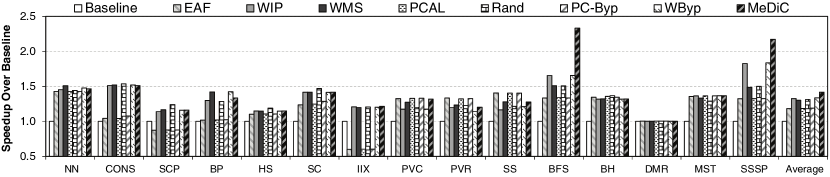
Baseline shows the performance of the unmodified GPU using FR-FCFS as the memory scheduler [357, 454]. EAF shows the performance of the Evicted-Address Filter [379]. WIP shows the performance of our warp-type-aware insertion policy by itself. WMS shows the performance of our warp-type-aware memory scheduling policy by itself. PCAL shows the performance of the PCAL bypassing mechanism proposed by Li et al. [247]. Rand shows the performance of a cache bypassing mechanism that performs bypassing decisions randomly on a fixed percentage of warps. PC-Byp shows the performance of the bypassing mechanism that uses the PC as the criterion for bypassing instead of the warp-type. WByp shows the performance of our warp-type-aware bypassing policy by itself.
From these secs/medic/results, we draw the following conclusions:
-
•
Each component of MeDiC individually provides significant performance improvement: WIP (32.5%), WMS (30.2%), and WByp (33.6%). MeDiC, which combines all three mechanisms, provides a 41.5% performance improvement over Baseline, on average. MeDiC matches or outperforms its individual components for all benchmarks except BP, where MeDiC has a higher L2 miss rate and lower row buffer locality than WMS and WByp.
- •
-
•
WMS provides significant performance gains (30.2%) over Baseline, because the memory scheduler prioritizes requests from warps that have a high hit ratio, allowing these warps to become active much sooner than they do in Baseline.
-
•
WByp provides an average 33.6% performance improvement over Baseline, because it is effective at reducing the L2 queuing latency. We show the change in queuing latency and provide a more detailed analysis in Section 4.5.3.
-
•
Compared to PCAL [247], WByp provides 12.8% better performance, and full MeDiC provides 21.8% better performance. We observe that while PCAL reduces the amount of cache thrashing, the reduction in thrashing does not directly translate into better performance. We observe that warps in the mostly-miss category sometimes have high reuse, and acquire tokens to access the cache. This causes less cache space to become available for mostly-hit warps, limiting how many of these warps become all-hit. However, when high-reuse warps that possess tokens are mainly in the mostly-hit category (PVC, PVR, SS, and BH), we find that PCAL performs better than WByp.
-
•
Compared to Rand,101010Note that our evaluation uses an ideal random bypassing mechanism, where we manually select the best individual percentage of requests to bypass the cache for each workload. As a result, the performance shown for Rand is better than can be practically realized. MeDiC performs 6.8% better, because MeDiC is able to make bypassing decisions that do not increase the miss rate significantly. This leads to lower off-chip bandwidth usage under MeDiC than under Rand. Rand increases the cache miss rate by 10% for the kernels of several applications (BP, PVC, PVR, BFS, and MST). We observe that in many cases, MeDiC improves the performance of applications that tend to generate a large number of memory requests, and thus experience substantial queuing latencies. We further analyze the effect of MeDiC on queuing delay in Section 4.5.3.
-
•
Compared to PC-Byp, MeDiC performs 12.4% better. We observe that the overhead of tracking the PC becomes significant, and that thrashing occurs as two PCs can hash to the same index, leading to inaccuracies in the bypassing decisions.
We conclude that each component of MeDiC, and the full MeDiC framework, are effective. Note that each component of MeDiC addresses the same problem (i.e., memory divergence of threads within a warp) using different techniques on different parts of the memory hierarchy. For the majority of workloads, one optimization is enough. However, we see that for certain high-intensity workloads (BFS and SSSP), the congestion is so high that we need to attack divergence on multiple fronts. Thus, MeDiC provides better average performance than all of its individual components, especially for such memory-intensive workloads.
4.5.2 Energy Efficiency of MeDiC
MeDiC provides significant GPU energy efficiency improvements, as shown in Figure 4.12. All three components of MeDiC, as well as the full MeDiC framework, are more energy efficient than all of the other works we compare against. MeDiC is 53.5% more energy efficient than Baseline. WIP itself is 19.3% more energy efficient than EAF. WMS is 45.2% more energy efficient than Baseline, which uses an FR-FCFS memory scheduler [357, 454]. WByp and MeDiC are more energy efficient than all of the other evaluated bypassing mechanisms, with 8.3% and 20.1% more efficiency than PCAL [247], respectively.
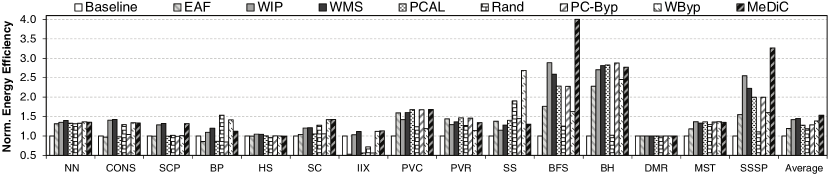
For all of our applications, the energy efficiency of MeDiC is better than or equal to Baseline, because even though our bypassing logic sometimes increases energy consumption by sending more memory requests to DRAM, the resulting performance improvement outweighs this additional energy. We also observe that our insertion policy reduces the L2 cache miss rate, allowing MeDiC to be even more energy efficient by not wasting energy on cache lookups for requests of all-miss warps.
4.5.3 Analysis of Benefits
Impact of MeDiC on Cache Miss Rate. One possible downside of cache bypassing is that the bypassed requests can introduce extra cache misses. Figure 4.13 shows the cache miss rate for Baseline, Rand, WIP, and MeDiC.
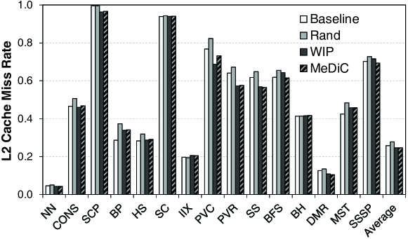
Unlike Rand, MeDiC does not increase the cache miss rate over Baseline for most of our applications. The key factor behind this is WIP, the insertion policy in MeDiC. We observe that WIP on its own provides significant cache miss rate reductions for several workloads (SCP, PVC, PVR, SS, and DMR). For the two workloads (BP and BFS) where WIP increases the miss rate (5% for BP, and 2.5% for BFS), the bypassing mechanism in MeDiC is able to contain the negative effects of WIP by dynamically tuning how aggressively bypassing is performed based on the change in cache miss rate (see Section 4.3.2). We conclude that MeDiC does not hurt the overall L2 cache miss rate.
Impact of MeDiC on Queuing Latency. Figure 4.14 shows the average L2 cache queuing latency for WByp and MeDiC, compared to Baseline queuing latency. For most workloads, WByp reduces the queuing latency significantly (up to 8.7x in the case of PVR). This reduction secs/medic/results in significant performance gains for both WByp and MeDiC.

There are two applications where the queuing latency increases significantly: BFS and SSSP. We observe that when cache bypassing is applied, the GPU cores retire instructions at a much faster rate (2.33x for BFS, and 2.17x for SSSP). This increases the pressure at each shared resource, including a sharp increase in the rate of cache requests arriving at the L2 cache. This additional backpressure secs/medic/results in higher L2 cache queuing latencies for both applications.
When all three mechanisms in MeDiC (bypassing, cache insertion, and memory scheduling) are combined, we observe that the queuing latency reduces even further. This additional reduction occurs because the cache insertion mechanism in MeDiC reduces the cache miss rate. We conclude that in general, MeDiC significantly alleviates the L2 queuing bottleneck.
Impact of MeDiC on Row Buffer Locality. Another possible downside of cache bypassing is that it may increase the number of requests serviced by DRAM, which in turn can affect DRAM row buffer locality. Figure 4.15 shows the row buffer hit rate for WMS and MeDiC, compared to the Baseline hit rate.
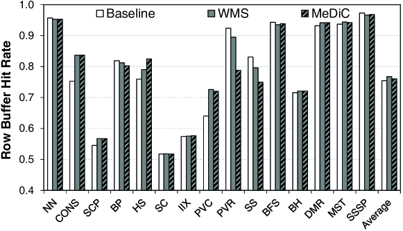
Compared to Baseline, WMS has a negative effect on the row buffer locality of six applications (NN, BP, PVR, SS, BFS, and SSSP), and a positive effect on seven applications (CONS, SCP, HS, PVC, BH, DMR, and MST). We observe that even though the row buffer locality of some applications decreases, the overall performance improves, as the memory scheduler prioritizes requests from warps that are more sensitive to long memory latencies. Additionally, prioritizing requests from warps that send a small number of memory requests (mostly-hit warps) over warps that send a large number of memory requests (mostly-miss warps) allows more time for mostly-miss warps to batch requests together, improving their row buffer locality. Prior work on GPU memory scheduling [33] has observed similar behavior, where batching requests together allows GPU requests to benefit more from row buffer locality.
4.5.4 Identifying Reuse in GPGPU Applications
While WByp bypasses warps that have low cache utility, it is possible that some cache blocks fetched by these bypassed warps get accessed frequently. Such a frequently-accessed cache block may be needed later by a mostly-hit warp, and thus leads to an extra cache miss (as the block bypasses the cache). To remedy this, we add a mechanism to MeDiC that ensures all high-reuse cache blocks still get to access the cache. The key idea, building upon the state-of-the-art mechanism for block-level reuse [379], is to use a Bloom filter to track the high-reuse cache blocks, and to use this filter to override bypassing decisions. We call this combined design MeDiC-reuse.
Figure 4.16 shows that MeDiC-reuse suffers 16.1% performance degradation over MeDiC. There are two reasons behind this degradation. First, we observe that MeDiC likely implicitly captures blocks with high reuse, as these blocks tend to belong to all-hit and mostly-hit warps. Second, we observe that several GPGPU applications contain access patterns that cause severe false positive aliasing within the Bloom filter used to implement EAF and MeDiC-reuse. This leads to some low reuse cache accesses from mostly-miss and all-miss warps taking up cache space unnecessarily, resulting in cache thrashing. We conclude that MeDiC likely implicitly captures the high reuse cache blocks that are relevant to improving memory divergence (and thus performance). However, there may still be room for other mechanisms that make the best of block-level cache reuse and warp-level heterogeneity in making caching decisions.
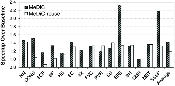
4.5.5 Hardware Cost
MeDiC requires additional metadata storage in two locations. First, each warp needs to maintain its own hit ratio. This can be done by adding 22 bits to the metadata of each warp: two 10-bit counters to track the number of L2 cache hits and the number of L2 cache accesses, and 2 bits to store the warp type.111111We combine the mostly-miss and all-miss categories into a single warp type value, because we perform the same actions on both types of warps. To efficiently account for overflow, the two counters that track L2 hits and L2 accesses are shifted right when the most significant bit of the latter counter is set. Additionally, the metadata for each cache line contains two bits, in order to annotate the warp type for the cache insertion policy. The total storage needed in the cache is NumCacheLines bits. In all, MeDiC comes at a cost of 5.1 kB, or less than 1% of the L2 cache size.
To evaluate the trade-off of storage overhead, we evaluate a GPU where this overhead is converted into additional L2 cache space for the baseline GPU. We conservatively increase the L2 capacity by 5%, and find that this additional cache capacity does not improve the performance of any of our workloads by more than 1%. As we discuss in the chapter, contention due to warp interference and divergence, and not due to cache capacity, is the root cause behind the performance bottlenecks that MeDiC alleviates. We conclude that MeDiC can deliver significant performance improvements with very low overhead.
4.6 MeDiC: Conclusion
Warps from GPGPU applications exhibit heterogeneity in their memory divergence behavior at the shared L2 cache within the GPU. We find that (1) some warps benefit significantly from the cache, while others make poor use of it; (2) such divergence behavior for a warp tends to remain stable for long periods of the warp’s execution; and (3) the impact of memory divergence can be amplified by the high queuing latencies at the L2 cache.
We propose Memory Divergence Correction (MeDiC), whose key idea is to identify memory divergence heterogeneity in hardware and use this information to drive cache management and memory scheduling, by prioritizing warps that take the greatest advantage of the shared cache. To achieve this, MeDiC consists of three warp-type-aware components for (1) cache bypassing, (2) cache insertion, and (3) memory scheduling. MeDiC delivers significant performance and energy improvements over multiple previously proposed policies, and over a state-of-the-art GPU cache management technique. We conclude that exploiting inter-warp heterogeneity is effective, and hope future works explore other ways of improving systems based on this key observation.
Chapter 5 Reducing Inter-application Interference with Staged Memory Scheduling
As the number of cores continues to increase in modern chip multiprocessor (CMP) systems, the DRAM memory system is becoming a critical shared resource. Memory requests from multiple cores interfere with each other, and this inter-application interference is a significant impediment to individual application and overall system performance. Previous work on application-aware memory scheduling [220, 221, 292, 293] has addressed the problem by making the memory controller aware of application characteristics and appropriately prioritizing memory requests to improve system performance and fairness.
Recent systems [62, 176, 307] present an additional challenge by introducing integrated graphics processing units (GPUs) on the same die with CPU cores. GPU applications typically demand significantly more memory bandwidth than CPU applications due to the GPU’s capability of executing a large number of parallel threads. GPUs use single-instruction multiple-data (SIMD) pipelines to concurrently execute multiple threads, where a batch of threads running the same instruction is called a wavefront or warp. When a wavefront stalls on a memory instruction, the GPU core hides this memory access latency by switching to another wavefront to avoid stalling the pipeline. Therefore, there can be thousands of outstanding memory requests from across all of the wavefronts. This is fundamentally more memory intensive than CPU memory traffic, where each CPU application has a much smaller number of outstanding requests due to the sequential execution model of CPUs.
Recent memory scheduling research has focused on memory interference between applications in CPU-only scenarios. These past proposals are built around a single centralized request buffer at each memory controller (MC). The scheduling algorithm implemented in the memory controller analyzes the stream of requests in the centralized request buffer to determine application memory characteristics, decides on a priority for each core, and then enforces these priorities. Observable memory characteristics may include the number of requests that result in row-buffer hits, the bank-level parallelism of each core, memory request rates, overall fairness metrics, and other information. Figure 5.1(a) shows the CPU-only scenario where the request buffer only holds requests from the CPUs. In this case, the memory controller sees a number of requests from the CPUs and has visibility into their memory behavior. On the other hand, when the request buffer is shared between the CPUs and the GPU, as shown in Figure 5.1(b), the large volume of requests from the GPU occupies a significant fraction of the memory controller’s request buffer, thereby limiting the memory controller’s visibility of the CPU applications’ memory behaviors.

One approach to increasing the memory controller’s visibility across a larger window of memory requests is to increase the size of its request buffer. This allows the memory controller to observe more requests from the CPUs to better characterize their memory behavior, as shown in Figure 5.1(c). For instance, with a large request buffer, the memory controller can identify and service multiple requests from one CPU core to the same row such that they become row-buffer hits, however, with a small request buffer as shown in Figure 5.1(b), the memory controller may not even see these requests at the same time because the GPU’s requests have occupied the majority of the entries.
Unfortunately, very large request buffers impose significant implementation challenges including the die area for the larger structures and the additional circuit complexity for analyzing so many requests, along with the logic needed for assignment and enforcement of priorities. Therefore, while building a very large, centralized memory controller request buffer could lead to good memory scheduling decisions, the approach is unattractive due to the resulting area, power, timing and complexity costs.
In this work, we propose the Staged Memory Scheduler (SMS), a decentralized architecture for memory scheduling in the context of integrated multi-core CPU-GPU systems. The key idea in SMS is to decouple the various functional requirements of memory controllers and partition these tasks across several simpler hardware structures which operate in a staged fashion. The three primary functions of the memory controller, which map to the three stages of our proposed memory controller architecture, are:
-
1.
Detection of basic within-application memory characteristics (e.g., row-buffer locality).
-
2.
Prioritization across applications (CPUs and GPU) and enforcement of policies to reflect the priorities.
-
3.
Low-level command scheduling (e.g., activate, precharge, read/write), enforcement of device timing constraints (e.g., t, t, etc.), and resolving resource conflicts (e.g., data bus arbitration).
Our specific SMS implementation makes widespread use of distributed FIFO structures to maintain a very simple implementation, but at the same time SMS can provide fast service to low memory-intensity (likely latency sensitive) applications and effectively exploit row-buffer locality and bank-level parallelism for high memory-intensity (bandwidth demanding) applications. While SMS provides a specific implementation, our staged approach for memory controller organization provides a general framework for exploring scalable memory scheduling algorithms capable of handling the diverse memory needs of integrated CPU-GPU systems of the future.
This work makes the following contributions:
-
•
We identify and present the challenges posed to existing memory scheduling algorithms due to the highly memory-bandwidth-intensive characteristics of GPU applications.
-
•
We propose a new decentralized, multi-stage approach to memory scheduling that effectively handles the interference caused by bandwidth-intensive applications, while simplifying the hardware implementation.
-
•
We evaluate our approach against four previous memory scheduling algorithms [357, 220, 293, 221] across a wide variety workloads and CPU-GPU systems and show that it provides better performance and fairness. As an example, our evaluations on a CPU-GPU system show that SMS improves system performance by 41.2% and fairness by 4.8 across 105 multi-programmed workloads on a 16-CPU/1-GPU, four memory controller system, compared to the best previous memory scheduler TCM [221].
5.1 Background
In this section, we re-iterate DRAM organization and discuss how past research attempted to deal with the challenges of providing performance and fairness for modern memory systems.
5.1.1 Main Memory Organization
DRAM is organized as two-dimensional arrays of bitcells. Reading or writing data to DRAM requires that a row of bitcells from the array first be read into a row buffer. This is required because the act of reading the row destroys the row’s contents, and so a copy of the bit values must be kept (in the row buffer). Reads and writes operate directly on the row buffer. Eventually the row is “closed” whereby the data in the row buffer are written back into the DRAM array. Accessing data already loaded in the row buffer, also called a row buffer hit, incurs a shorter latency than when the corresponding row must first be “opened” from the DRAM array. A modern memory controller (MC) must orchestrate the sequence of commands to open, read, write and close rows. Servicing requests in an order that increases row-buffer hits tends to improve overall throughput by reducing the average latency to service requests. The MC is also responsible for enforcing a wide variety of timing constraints imposed by modern DRAM standards (e.g., DDR3) such as limiting the rate of page-open operations (t) and ensuring a minimum amount of time between writes and reads (t).
Each two dimensional array of DRAM cells constitutes a bank, and a group of banks form a rank. All banks within a rank share a common set of command and data buses, and the memory controller is responsible for scheduling commands such that each bus is used by only one bank at a time. Operations on multiple banks may occur in parallel (e.g., opening a row in one bank while reading data from another bank’s row buffer) so long as the buses are properly scheduled and any other DRAM timing constraints are honored. A memory controller can improve memory system throughput by scheduling requests such that bank-level parallelism or BLP (i.e., the number of banks simultaneously busy responding to commands) is increased. A memory system implementation may support multiple independent memory channels (each with its own ranks and banks) to further increase the number of memory requests that can be serviced at the same time. A key challenge in the implementation of modern, high-performance memory controllers is to effectively improve system performance by maximizing both row-buffer hits and BLP while simultaneously providing fairness among multiple CPUs and the GPU.
5.1.2 Memory Scheduling
Accessing off-chip memory is one of the major bottlenecks in microprocessors. Requests that miss in the last level cache incur long latencies, and as multi-core processors increase the number of CPUs, the problem gets worse because all of the cores must share the limited off-chip memory bandwidth. The large number of requests greatly increases contention for the memory data and command buses. Since a bank can only process one command at a time, the large number of requests also increases bank contention where requests must wait for busy banks to finish servicing other requests. A request from one core can also cause a row buffer containing data for another core to be closed, thereby reducing the row-buffer hit rate of that other core (and vice-versa). All of these effects increase the latency of memory requests by both increasing queuing delays (time spent waiting for the memory controller to start servicing a request) and DRAM device access delays (due to decreased row-buffer hit rates and bus contention).
The memory controller is responsible for buffering and servicing memory requests from the different cores and the GPU. Typical implementations make use of a memory request buffer to hold and keep track of all in-flight requests. Scheduling logic then decides which requests should be serviced, and issues the corresponding commands to the DRAM devices. Different memory scheduling algorithms may attempt to service memory requests in an order different than the order in which the requests arrived at the memory controller, in order to increase row-buffer hit rates, bank level parallelism, fairness, or achieve other goals.
5.1.3 Memory Scheduling in CPU-only Systems
Memory scheduling algorithms improve system performance by reordering memory requests to deal with the different constraints and behaviors of DRAM. The first-ready-first-come-first-serve (FR-FCFS) [357] algorithm attempts to schedule requests that result in row-buffer hits (first-ready), and otherwise prioritizes older requests (FCFS). FR-FCFS increases DRAM throughput, but it can cause fairness problems by under-servicing applications with low row-buffer locality. Several application-aware memory scheduling algorithms [220, 221, 292, 293] have been proposed to balance both performance and fairness. Parallelism-aware Batch Scheduling (PAR-BS) [293] batches requests based on their arrival times (older requests batched first). Within a batch, applications are ranked to preserve bank-level parallelism (BLP) within an application’s requests. More recently, ATLAS [220] proposes prioritizing applications that have received the least memory service. As a result, applications with low memory intensities, which typically attain low memory service, are prioritized. However, applications with high memory intensities are deprioritized and hence slowed down significantly, resulting in unfairness. The most recent work on application-aware memory scheduling, Thread Cluster Memory scheduling (TCM) [221], addresses this unfairness problem. TCM first clusters applications into low and high memory-intensity clusters based on their memory intensities. TCM always prioritizes applications in the low memory-intensity cluster, however, among the high memory-intensity applications it shuffles request priorities to prevent unfairness.
5.1.4 Characteristics of Memory Accesses from GPUs
A typical CPU application only has a relatively small number of outstanding memory requests at any time. The size of a processor’s instruction window bounds the number of misses that can be simultaneously exposed to the memory system. Branch prediction accuracy limits how large the instruction window can be usefully increased. In contrast, GPU applications have very different access characteristics, generating many more memory requests than CPU applications. A GPU application can consist of many thousands of parallel threads, where memory stalls on one group of threads can be hidden by switching execution to one of the many other groups of threads.
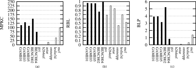
Figure 5.2 (a) shows the memory request rates for a representative subset of our GPU applications and the most memory-intensive SPEC2006 (CPU) applications, as measured by memory requests per thousand cycles (see Section 5.3.5 for simulation methodology descriptions) when each application runs alone on the system. The raw bandwidth demands of the GPU applications are often multiple times higher than the SPEC benchmarks. Figure 5.2 (b) shows the row-buffer hit rates (also called row-buffer locality or RBL). The GPU applications show consistently high levels of RBL, whereas the SPEC benchmarks exhibit more variability. The GPU programs have high levels of spatial locality, often due to access patterns related to large sequential memory accesses (e.g., frame buffer updates). Figure 5.2(c) shows the BLP for each application, with the GPU programs consistently making use of far banks at the same time.
In addition to the high-intensity memory traffic of GPU applications, there are other properties that distinguish GPU applications from CPU applications. The TCM [221] study observed that CPU applications with streaming access patterns typically exhibit high RBL but low BLP, while applications with less uniform access patterns typically have low RBL but high BLP. In contrast, GPU applications have both high RBL and high BLP. The combination of high memory intensity, high RBL and high BLP means that the GPU will cause significant interference to other applications across all banks, especially when using a memory scheduling algorithm that preferentially favors requests that result in row-buffer hits.
5.1.5 What Has Been Done in the GPU?
As opposed to CPU applications, GPU applications are not very latency sensitive as there are a large number of independent threads to cover long memory latencies. However, the GPU requires a significant amount of bandwidth far exceeding even the most memory-intensive CPU applications. As a result, a GPU memory scheduler [251] typically needs a large request buffer that is capable of request coalescing (i.e., combining multiple requests for the same block of memory into a single combined request [313]). Furthermore, since GPU applications are bandwidth intensive, often with streaming access patterns, a policy that maximizes the number of row-buffer hits is effective for GPUs to maximize overall throughput. As a result, FR-FCFS with a large request buffer tends to perform well for GPUs [46]. In view of this, previous work [445] designed mechanisms to reduce the complexity of row-hit first based (FR-FCFS) scheduling.
5.2 Challenges with Existing Memory Controllers
5.2.1 The Need for Request Buffer Capacity
The results from Figure 5.2 showed that GPU applications have very high memory intensities. As discussed in Section 2.2.1, the large number of GPU memory requests occupy many of the memory controller’s request buffer entries, thereby making it very difficult for the memory controller to properly determine the memory access characteristics of each of the CPU applications. Figure 5.3 shows the performance impact of increasing the memory controller’s request buffer size for a variety of memory scheduling algorithms (full methodology details can be found in Section 5.3.5) for a 16-CPU/1-GPU system. By increasing the size of the request buffer from 64 entries to 256 entries,111For all sizes, half of the entries are reserved for the CPU requests. previously proposed memory controller algorithms can gain up to 63.6% better performance due to this improved visibility.

5.2.2 Implementation Challenges in Providing Request Buffer Capacity
The results above show that when the memory controller has enough visibility across the global memory request stream to properly characterize the behaviors of each core, a sophisticated algorithm like TCM can be effective at making good scheduling decisions. Unfortunately, implementing a sophisticated algorithm like TCM over such a large scheduler introduces very significant implementation challenges. For all algorithms that use a centralized request buffer and prioritize requests that result in row-buffer hits (FR-FCFS, PAR-BS, ATLAS, TCM), associative logic (CAMs) will be needed for each entry to compare its requested row against currently open rows in the DRAM banks. For all algorithms that prioritize requests based on rank/age (FR-FCFS, PAR-BS, ATLAS, TCM), a large comparison tree is needed to select the highest ranked/oldest request from all request buffer entries. The size of this comparison tree grows with request buffer size. Furthermore, in addition to this logic for reordering requests and enforcing ranking/age, TCM also requires additional logic to continually monitor each CPU’s last-level cache MPKI rate (note that a CPU’s instruction count is not typically available at the memory controller), each core’s RBL which requires additional shadow row buffer index tracking [100, 102], and each core’s BLP.
Apart from the logic required to implement the policies of the specific memory scheduling algorithms, all of these memory controller designs need additional logic to enforce DDR timing constraints. Note that different timing constraints will apply depending on the state of each memory request. For example, if a memory request’s target bank currently has a different row loaded in its row buffer, then the memory controller must ensure that a precharge (row close) command is allowed to issue to that bank (e.g., has t elapsed since the row was opened?), but if the row is already closed, then different timing constraints will apply. For each request buffer entry, the memory controller will determine whether or not the request can issue a command to the DRAM based on the current state of the request and the current state of the DRAM system. That is, every request buffer entry (i.e., all 256) needs an independent instantiation of the DDR compliance-checking logic (including data and command bus availability tracking). This type of monolithic memory controller effectively implements a large out-of-order scheduler; note that typical instruction schedulers in modern out-of-order processors only have about 32-64 entries [117]. Even after accounting for the clock speed differences between CPU core and DRAM command frequencies, it is very difficult to implement a fully-associative222Fully associative in the sense that a request in any one of the request buffer entries could be eligible to issue in a given cycle., age-ordered/prioritized, out-of-order scheduler with 256-512 entries [324].
5.3 The Staged Memory Scheduler
The proposed Staged Memory Scheduler (SMS) is structured to reflect the primary functional tasks of the memory scheduler. Below, we first describe the overall SMS algorithm, explain additional implementation details, step through the rationale for the design, and then walk through the hardware implementation.
5.3.1 The SMS Algorithm
Batch Formation. The first stage of SMS consists of several simple FIFO structures, one per source (i.e., a CPU core or the GPU). Each request from a given source is initially inserted into its respective FIFO upon arrival at the memory controller. A batch is simply one or more memory requests from the same source that access the same DRAM row. That is, all requests within a batch, except perhaps for the first one, would be row-buffer hits if scheduled consecutively. A batch is complete or ready when an incoming request accesses a different row, when the oldest request in the batch has exceeded a threshold age, or when the FIFO is full. Ready batches may then be considered by the second stage of the SMS.
Batch Scheduler. The batch formation stage has combined individual memory requests into batches of row-buffer hitting requests. The next stage, the batch scheduler, deals directly with batches, and therefore need not worry about scheduling to optimize for row-buffer locality. Instead, the batch scheduler can focus on higher-level policies regarding inter-application interference and fairness. The goal of the batch scheduler is to prioritize batches from applications that are latency critical, while making sure that bandwidth-intensive applications (e.g., the GPU) still make reasonable progress.
The batch scheduler operates in two states: pick and drain. In the pick state, the batch scheduler considers each FIFO from the batch formation stage. For each FIFO that contains a ready batch, the batch scheduler picks one batch based on a balance of shortest-job first (SJF) and round-robin principles. For SJF, the batch scheduler chooses the core (or GPU) with the fewest total memory requests across all three stages of the SMS. SJF prioritization reduces average request service latency, and it tends to favor latency-sensitive applications, which tend to have fewer total requests. The other component of the batch scheduler is a round-robin policy that simply cycles through each of the per-source FIFOs ensuring that high memory-intensity applications receive adequate service. Overall, the batch scheduler chooses the SJF policy with a probability of , and the round-robin policy otherwise.
After picking a batch, the batch scheduler enters a drain state where it forwards the requests from the selected batch to the final stage of the SMS. The batch scheduler simply dequeues one request per cycle until all requests from the batch have been removed from the selected batch formation FIFO. At this point, the batch scheduler re-enters the pick state to select the next batch.
DRAM Command Scheduler. The last stage of the SMS is the DRAM command scheduler (DCS). The DCS consists of one FIFO queue per DRAM bank (e.g., eight banks/FIFOs for DDR3). The drain phase of the batch scheduler places the memory requests directly into these FIFOs. Note that because batches are moved into the DCS FIFOs one batch at a time, any row-buffer locality within a batch is preserved within a DCS FIFO. At this point, any higher-level policy decisions have already been made by the batch scheduler, therefore, the DCS can simply focus on issuing low-level DRAM commands and ensuring DDR protocol compliance.
On any given cycle, the DCS only considers the requests at the head of each of the per-bank FIFOs. For each request, the DCS determines whether that request can issue a command based on the request’s current row-buffer state (i.e., is the row buffer already open with the requested row, closed, or open with the wrong row?) and the current DRAM state (e.g., time elapsed since a row was opened in a bank, data bus availability). If more than one request is eligible to issue a command, the DCS simply arbitrates in a round-robin fashion.
5.3.2 Additional Algorithm Details
Batch Formation Thresholds. The batch formation stage holds requests in the per-source FIFOs until a complete batch is ready. This could unnecessarily delay requests as the batch will not be marked ready until a request to a different row arrives at the memory controller, or the FIFO size has been reached. This additional queuing delay can be particularly devastating for low-intensity, latency-sensitive applications.
SMS considers an application’s memory intensity in forming batches. For applications with low memory-intensity (1 MPKC), SMS completely bypasses the batch formation and batch scheduler, and forwards requests directly to the DCS per-bank FIFOs. For these highly sensitive applications, such a bypass policy minimizes the delay to service their requests. Note that this bypass operation will not interrupt an on-going drain from the batch scheduler, which ensures that any separately scheduled batches maintain their row-buffer locality.
For medium memory-intensity (1-10 MPKC) and high memory-intensity (10 MPKC) applications, the batch formation stage uses age thresholds of 50 and 200 cycles, respectively. That is, regardless of how many requests are in the current batch, when the oldest request’s age exceeds the threshold, the entire batch is marked ready (and consequently, any new requests that arrive, even if accessing the same row, will be grouped into a new batch). Note that while TCM uses the MPKI metric to classify memory intensity, SMS uses misses per thousand cycles (MPKC) since the per-application instruction counts are not typically available in the memory controller. While it would not be overly difficult to expose this information, this is just one less implementation overhead that SMS can avoid.
Global Bypass. As described above, low memory-intensity applications can bypass the entire batch formation and scheduling process and proceed directly to the DCS. Even for high memory-intensity applications, if the memory system is lightly loaded (e.g., if this is the only application running on the system right now), then the SMS will allow all requests to proceed directly to the DCS. This bypass is enabled whenever the total number of in-flight requests (across all sources) in the memory controller is less than sixteen requests.
Round-Robin Probability. As described above, the batch scheduler uses a probability of to schedule batches with the SJF policy and the round-robin policy otherwise. Scheduling batches in a round-robin order can ensure fair progress from high-memory intensity applications. Our experimental results show that setting to 90% (10% using the round-robin policy) provides a good performance-fairness trade-off for SMS.
5.3.3 SMS Rationale
In-Order Batch Formation. It is important to note that batch formation occurs in the order of request arrival. This potentially sacrifices some row-buffer locality as requests to the same row may be interleaved with requests to other rows. We considered many variations of batch formation that allowed out-of-order grouping of requests to maximize the length of a run of row-buffer hitting requests, but the overall performance benefit was not significant. First, constructing very large batches of row-buffer hitting requests can introduce significant unfairness as other requests may need to wait a long time for a bank to complete its processing of a long run of row-buffer hitting requests [205]. Second, row-buffer locality across batches may still be exploited by the DCS. For example, consider a core that has three batches accessing row X, row Y, and then row X again. If X and Y map to different DRAM banks, say banks A and B, then the batch scheduler will send the first and third batches (row X) to bank A, and the second batch (row Y) to bank B. Within the DCS’s FIFO for bank A, the requests for the first and third batches will all be one after the other, thereby exposing the row-buffer locality across batches despite the requests appearing “out-of-order” in the original batch formation FIFOs.
In-Order Batch Scheduling. Due to contention and back-pressure in the system, it is possible that a FIFO in the batch formation stage contains more than one valid batch. In such a case, it could be desirable for the batch scheduler to pick one of the batches not currently at the head of the FIFO. For example, the bank corresponding to the head batch may be busy while the bank for another batch is idle. Scheduling batches out of order could decrease the service latency for the later batches, but in practice it does not make a big difference and adds significant implementation complexity. It is important to note that even though batches are dequeued from the batch formation stage in arrival order per FIFO, the request order between the FIFOs may still slip relative to each other. For example, the batch scheduler may choose a recently arrived (and formed) batch from a high-priority (i.e., latency-sensitive) source even though an older, larger batch from a different source is ready.
In-Order DRAM Command Scheduling. For each of the per-bank FIFOs in the DCS, the requests are already grouped by row-buffer locality (because the batch scheduler drains an entire batch at a time), and globally ordered to reflect per-source priorities. Further reordering at the DCS would likely just undo the prioritization decisions made by the batch scheduler. Like the batch scheduler, the in-order nature of each of the DCS per-bank FIFOs does not prevent out-of-order scheduling at the global level. A CPU’s requests may be scheduled to the DCS in arrival order, but the requests may get scattered across different banks, and the issue order among banks may slip relative to each other.
5.3.4 Hardware Implementation
The staged architecture of SMS lends directly to a low-complexity
hardware implementation. Figure 5.4 illustrates the overall
hardware organization of SMS.
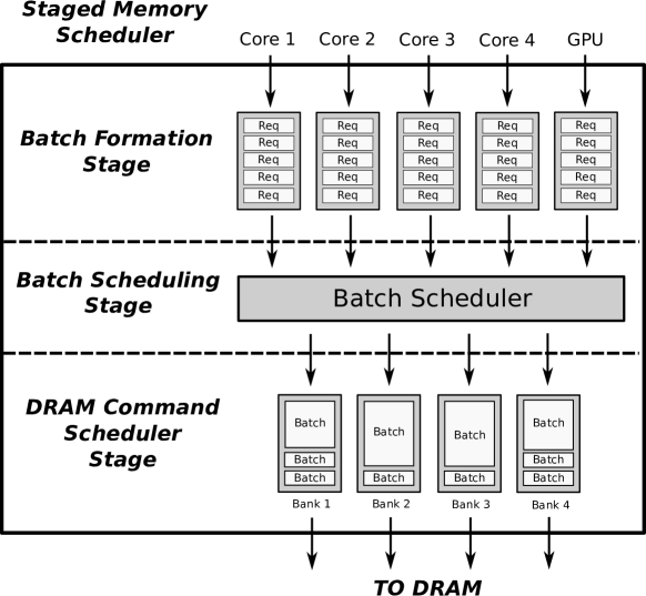
Batch Formation. The batch formation stage consists of
little more than one FIFO per source (CPU or GPU). Each FIFO maintains
an extra register that records the row index of the last request, so
that any incoming request’s row index can be compared to determine if
the request can be added to the existing batch. Note that this requires
only a single comparator (used only once at insertion) per FIFO. Contrast
this to a conventional monolithic request buffer where comparisons on
every request buffer entry (which is much larger than the number of FIFOs that SMS uses) must be made, potentially against all currently open rows across all
banks.
Batch Scheduler. The batch scheduling stage consists primarily
of combinatorial logic to implement the batch picking rules. When using the
SJF policy, the batch scheduler only needs to pick the batch corresponding to
the source with the fewest in-flight requests, which can be easily performed
with a tree of MIN operators. Note that this tree is relatively shallow since
it only grows as a function of the number of FIFOs. Contrast this to the
monolithic scheduler where the various ranking trees grow as a function of the
total number of entries.
DRAM Command Scheduler. The DCS stage consists of the per-bank
FIFOs. The logic to track and enforce the various DDR timing and power
constraints is identical to the case of the monolithic scheduler, but the scale
is drastically different. The DCS’s DDR command-processing logic only considers the
requests at the head of each of the per-bank FIFOs (eight total for DDR3),
whereas the monolithic scheduler requires logic to consider every request buffer entry (hundreds).
Overall Configuration and Hardware Cost. The final configuration of SMS that we use in this dissertation consists of the following hardware structures. The batch formation stage uses ten-entry FIFOs for each of the CPU cores, and a twenty-entry FIFO for the GPU. The DCS uses a fifteen-entry FIFO for each of the eight DDR3 banks. For sixteen cores and a GPU, the aggregate capacity of all of these FIFOs is 300 requests, although at any point in time, the SMS logic can only consider or act on a small subset of the entries (i.e., the seventeen at the heads of the batch formation FIFOs and the eight at the heads of the DCS FIFOs). In addition to these primary structures, there are a small handful of bookkeeping counters. One counter per source is needed to track the number of in-flight requests; each counter is trivially managed as it only needs to be incremented when a request arrives at the memory controller, and then decremented when the request is complete. Counters are also needed to track per-source MPKC rates for memory-intensity classification, which are incremented when a request arrives, and then periodically reset. Table 5.1 summarizes the amount of hardware overhead required for each stage of SMS.
| Storage | Description | Size |
| Storage Overhead of Stage 1: Batch formation stage | ||
| CPU FIFO queues | A CPU core’s FIFO queue | entries |
| GPU FIFO queues | A GPU’s FIFO queue | entries |
| MPKC counters | Counts per-core MPKC | bits |
| Last request’s row index | Stores the row index of | bits |
| the last request to the FIFO | ||
| Storage Overhead of Stage 2: Batch Scheduler | ||
| CPU memory request counters | Counts the number of outstanding | bits |
| memory requests of a CPU core | ||
| GPU memory request counter | Counts the number of outstanding | bits |
| memory requests of the GPU | ||
| Storage Overhead of Stage 3: DRAM Command Scheduler | ||
| Per-Bank FIFO queues | Contains a FIFO queue per bank | entries |
5.3.5 Experimental Methodology
We use an in-house cycle-accurate simulator to perform our evaluations. For our performance evaluations, we model a system with sixteen x86 CPU cores and a GPU. For the CPUs, we model three-wide out-of-order processors with a cache hierarchy including per-core L1 caches and a shared, distributed L2 cache. The GPU does not share the CPU caches. Table 5.2 shows the detailed system parameters for the CPU and GPU cores. The parameters for the main memory system are listed in Table 5.2. Unless stated otherwise, we use four memory controllers (one channel per memory controller) for all experiments. In order to prevent the GPU from taking the majority of request buffer entries, we reserve half of the request buffer entries for the CPUs. To model the memory bandwidth of the GPU accurately, we perform coalescing on GPU memory requests before they are sent to the memory controller [251].
| Parameter | Setting |
|---|---|
| CPU Clock Speed | 3.2GHz |
| CPU ROB | 128 entries |
| CPU L1 cache | 32KB Private, 4-way |
| CPU L2 cache | 8MB Shared, 16-way |
| CPU Cache Rep. Policy | LRU |
| GPU SIMD Width | 800 |
| GPU Texture units | 40 |
| GPU Z units | 64 |
| GPU Color units | 16 |
| Memory Controller Entries | 300 |
| Channels/Ranks/Banks | 4/1/8 |
| DRAM Row buffer size | 2KB |
| DRAM Bus | 128 bits/channel |
| tRCD/tCAS/tRP | 8/8/8 ns |
| tRAS/tRC/tRRD | 20/27/4 ns |
| tWTR/tRTP/tWR | 4/4/6 ns |
Workloads. We evaluate our system with a set of 105 multiprogrammed workloads, each simulated for 500 million cycles. Each workload consists of sixteen SPEC CPU2006 benchmarks and one GPU application selected from a mix of video games and graphics performance benchmarks. For each CPU benchmark, we use PIN [355, 261] with PinPoints [328] to select the representative phase. For the GPU application, we use an industrial GPU simulator to collect memory requests with detailed timing information. These requests are collected after having first been filtered through the GPU’s internal cache hierarchy, therefore we do not further model any caches for the GPU in our final hybrid CPU-GPU simulation framework.
We classify CPU benchmarks into three categories (Low, Medium, and High) based on their memory intensities, measured as last-level cache misses per thousand instructions (MPKI). Table 5.3 shows the MPKI for each CPU benchmark. Benchmarks with less than 1 MPKI are low memory-intensive, between 1 and 25 MPKI are medium memory-intensive, and greater than 25 are high memory-intensive. Based on these three categories, we randomly choose a number of benchmarks from each category to form workloads consisting of seven intensity mixes: L (All low), ML (Low/Medium), M (All medium), HL (High/Low), HML (High/Medium/Low), HM (High/Medium) and H(All high). The GPU benchmark is randomly selected for each workload without any classification.
| Name | MPKI | Name | MPKI | Name | MPKI |
|---|---|---|---|---|---|
| tonto | 0.01 | sjeng | 1.08 | omnetpp | 21.85 |
| povray | 0.01 | gobmk | 1.19 | milc | 21.93 |
| calculix | 0.06 | gromacs | 1.67 | xalancbmk | 22.32 |
| perlbench | 0.11 | h264ref | 1.86 | libquantum | 26.27 |
| namd | 0.11 | bzip2 | 6.08 | leslie3d | 38.13 |
| dealII | 0.14 | astar | 7.6 | soplex | 52.45 |
| wrf | 0.21 | hmmer | 8.65 | GemsFDTD | 63.61 |
| gcc | 0.33 | cactusADM | 14.99 | lbm | 69.63 |
| sphinx3 | 17.24 | mcf | 155.30 |
Performance Metrics. In an integrated CPUs and GPU system like the one we evalute, To measure system performance, we use CPU+GPU Weighted Speedup (Eqn. 5.1), which is a sum of the CPU weighted speedup [108, 107] and the GPU speedup multiply by the weight of the GPU. In addition, we measure Unfairness [93, 220, 221, 418] using maximum slowdown for all the CPU cores. We report the harmonic mean instead of arithmetic mean for Unfairness in our evaluations since slowdown is an inverse metric of speedup.
| (5.1) |
| (5.2) |
5.4 Qualitative Comparison with Previous Scheduling Algorithms
In this section, we compare SMS qualitatively to previously proposed scheduling policies and analyze the basic differences between SMS and these policies. The fundamental difference between SMS and previously proposed memory scheduling policies for CPU only scenarios is that the latter are designed around a single, centralized request buffer which has poor scalability and complex scheduling logic, while SMS is built around a decentralized, scalable framework.
5.4.1 First-Ready FCFS (FR-FCFS)
FR-FCFS [357] is a commonly used scheduling policy in commodity DRAM systems. A FR-FCFS scheduler prioritizes requests that result in row-buffer hits over row-buffer misses and otherwise prioritizes older requests. Since FR-FCFS unfairly prioritizes applications with high row-buffer locality to maximize DRAM throughput, prior work [220, 293, 221, 292, 281] have observed that it has low system performance and high unfairness.
5.4.2 Parallelism-aware Batch Scheduling (PAR-BS)
PAR-BS [293] aims to improve fairness and system performance. In order to prevent unfairness, it forms batches of outstanding memory requests and prioritizes the oldest batch, to avoid request starvation. To improve system throughput, it prioritizes applications with smaller number of outstanding memory requests within a batch. However, PAR-BS has two major shortcomings. First, batching could cause older GPU requests and requests of other memory-intensive CPU applications to be prioritized over latency-sensitive CPU applications. Second, as previous work [220] has also observed, PAR-BS does not take into account an application’s long term memory-intensity characteristics when it assigns application priorities within a batch. This could cause memory-intensive applications’ requests to be prioritized over latency-sensitive applications’ requests within a batch.
5.4.3 Adaptive per-Thread Least-Attained-Serviced Memory Scheduling (ATLAS)
ATLAS [220] aims to improve system performance by prioritizing requests of applications with lower attained memory service. This improves the performance of low memory-intensity applications as they tend to have low attained service. However, ATLAS has the disadvantage of not preserving fairness. Previous work [220, 221] have shown that simply prioritizing low memory intensity applications leads to significant slowdown of memory-intensive applications.
5.4.4 Thread Cluster Memory Scheduling (TCM)
TCM [221] is the best state-of-the-art application-aware memory scheduler providing both system throughput and fairness. It groups applications into either latency- or bandwidth-sensitive clusters based on their memory intensities. In order to achieve high system throughput and low unfairness, TCM employs different prioritization policy for each cluster. To improve system throughput, a fraction of total memory bandwidth is dedicated to latency-sensitive cluster and applications within the cluster are then ranked based on memory intensity with least memory-intensive application receiving the highest priority. On the other hand, TCM minimizes unfairness by periodically shuffling applications within a bandwidth-sensitive cluster to avoid starvation. This approach provides both high system performance and fairness in CPU-only systems. In an integrated CPU-GPU system, GPU generates a significantly larger amount of memory requests compared to CPUs and fills up the centralized request buffer. As a result, the memory controller lacks the visibility of CPU memory requests to accurately determine each application’s memory access behavior. Without the visibility, TCM makes incorrect and non-robust clustering decisions, which classify some applications with high memory intensity into the latency-sensitive cluster. These misclassified applications cause interference not only to low memory intensity applications, but also to each other. Therefore, TCM causes some degradation in both system performance and fairness in an integrated CPU-GPU system. As described in Section 5.2, increasing the request buffer size is a simple and straightforward way to gain more visibility into CPU applications’ memory access behaviors. However, this approach is not scalable as we show in our evaluations (Section 6.6). In contrast, SMS provides much better system performance and fairness than TCM with the same number of request buffer entries and lower hardware cost.
5.5 Experimental Evaluation of SMS
We present the performance of five memory scheduler configurations: FR-FCFS, ATLAS, PAR-BS, TCM, and SMS on the 16-CPU/1-GPU four-memory-controller system described in Section 5.3.5. All memory schedulers use 300 request buffer entries per memory controller; this size was chosen based on the results in Figure 5.3 which showed that performance does not appreciably increase for larger request buffer sizes. Results are presented in the workload categories as described in Section 5.3.5, with workload memory intensities increasing from left to right.
Figure 5.5 shows the system performance (measured as weighted speedup) and fairness of the previously proposed algorithms and SMS, averaged across 15 workloads for each of the seven categories (105 workloads in total). Compared to TCM, which is the best previous algorithm for both system performance and fairness, SMS provides 41.2% system performance improvement and 4.8 fairness improvement. Therefore, we conclude that SMS provides better system performance and fairness than all previously proposed scheduling policies, while incurring much lower hardware cost and simpler scheduling logic.
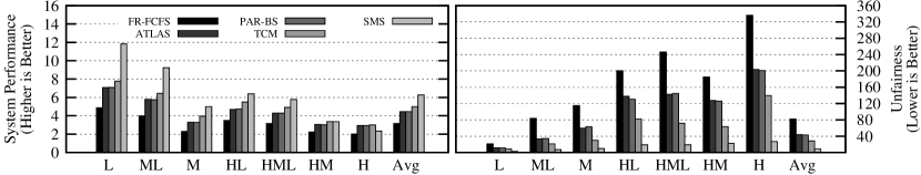
Based on the results for each workload category, we make the following major observations: First, SMS consistently outperforms previously proposed algorithms (given the same number of request buffer entries), in terms of both system performance and fairness across most of the workload categories. Second, in the “H” category with only high memory-intensity workloads, SMS underperforms by 21.2%/20.7%/22.3% compared to ATLAS/PAR-BS/TCM, but SMS still provides 16.3% higher system performance compared to FR-FCFS. The main reason for this behavior is that ATLAS/PAR-BS/TCM improve performance by unfairly prioritizing certain applications over others, which is reflected by their poor fairness results. For instance, we observe that TCM misclassifies some of these high memory-intensity applications into the low memory-intensity cluster, which starves requests of applications in the high memory-intensity cluster. On the other hand, SMS preserves fairness in all workload categories by using its probabilistic round-robin policy as described in Section 5.3. As a result, SMS provides 7.6/7.5/5.2 better fairness relative to ATLAS/PAR-BS/TCM respectively, for the high memory-intensity category.
5.5.1 Analysis of CPU and GPU Performance
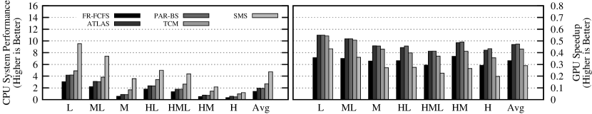
In this section, we study the performance of the CPU system and the GPU system separately. Figure 5.6 shows CPU-only weighted speedup and GPU speedup. Two major observations are in order. First, SMS gains 1.76 improvement in CPU system performance over TCM. Second, SMS achieves this 1.76 CPU performance improvement while delivering similar GPU performance as the FR-FCFS baseline.333Note that our GPU Speedup metric is defined with respect to the performance of the GPU benchmark running on the system by itself. In all cases, the relative speedup reported is much less than 1.0 because the GPU must now share memory bandwidth with 16 CPUs. The results show that TCM (and the other algorithms) end up allocating far more bandwidth to the GPU, at significant performance and fairness cost to the CPU applications. SMS appropriately deprioritizes the memory bandwidth intensive GPU application in order to enable higher CPU performance and overall system performance, while preserving fairness. Previously proposed scheduling algorithms, on the other hand, allow the GPU to hog memory bandwidth and significantly degrade system performance and fairness (Figure 5.5).
5.5.2 Scalability with Cores and Memory Controllers

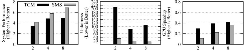
Figure 5.7 compares the performance and fairness of SMS against TCM (averaged over 75 workloads444We use 75 randomly selected workloads per core count. We could not use the same workloads/categorizations as earlier because those were for 16-core systems, whereas we are now varying the number of cores.) with the same number of request buffers, as the number of cores is varied. We make the following observations: First, SMS continues to provide better system performance and fairness than TCM. Second, the system performance gains and fairness gains increase significantly as the number of cores and hence, memory pressure is increased. SMS’s performance and fairness benefits are likely to become more significant as core counts in future technology nodes increase.
Figure 5.8 shows the system performance and fairness of SMS compared against TCM as the number of memory channels is varied. For this, and all subsequent results, we perform our evaluations on 60 workloads from categories that contain high memory-intensity applications. We observe that SMS scales better as the number of memory channels increases. As the performance gain of TCM diminishes when the number of memory channels increases from 4 to 8 channels, SMS continues to provide performance improvement for both CPU and GPU.
5.5.3 Sensitivity to SMS Design Parameters
Effect of Batch Formation. Figure 5.10 shows the system performance and fairness of SMS as the maximum batch size varies. When the batch scheduler can forward individual requests to the DCS, the system performance and fairness drops significantly by 12.3% and 1.9 compared to when it uses a maximum batch size of ten. The reasons are twofold: First, intra-application row-buffer locality is not preserved without forming requests into batches and this causes performance degradation due to longer average service latencies. Second, GPU and high memory-intensity applications’ requests generate a lot of interference by destroying each other’s and most importantly latency-sensitive applications’ row-buffer locality. With a reasonable maximum batch size (starting from ten onwards), intra-application row-buffer locality is well-preserved with reduced interference to provide good system performance and fairness. We have also observed that most CPU applications rarely form batches that exceed ten requests. This is because the in-order request stream rarely has such a long sequence of requests all to the same row, and the timeout threshold also prevents the batches from becoming too large. As a result, increasing the batch size beyond ten requests does not provide any extra benefit, as shown in Figure 5.10.
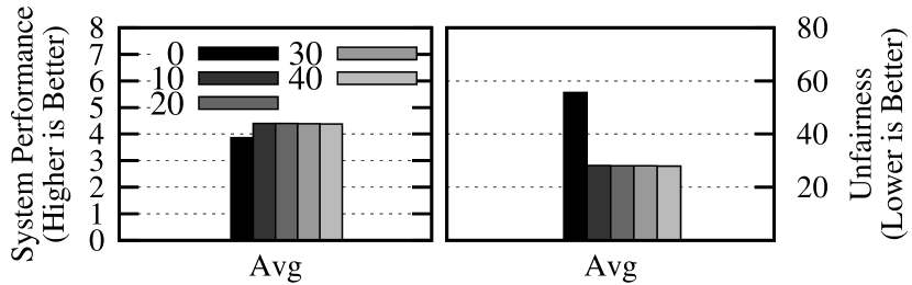
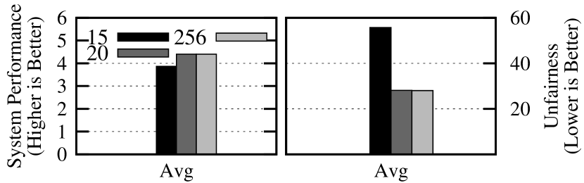
DCS FIFO Size. Figure 5.10 shows the sensitivity of SMS to the size of the per-bank FIFOs in the DRAM Command Scheduler (DCS). Fairness degrades as the size of the DCS FIFOs is increased. As the size of the per-bank DCS FIFOs increases, the batch scheduler tends to move more batches from the batch formation stage to the DCS FIFOs. Once batches are moved to the DCS FIFOs, they cannot be reordered anymore. So even if a higher-priority batch were to become ready, the batch scheduler cannot move it ahead of any batches already in the DCS. On the other hand, if these batches were left in the batch formation stage, the batch scheduler could still reorder them. Overall, it is better to employ smaller per-bank DCS FIFOs that leave more batches in the batch formation stage, enabling the batch scheduler to see more batches and make better batch scheduling decisions, thereby reducing starvation and improving fairness. The FIFOs only need to be large enough to keep the DRAM banks busy.
5.5.4 Case Studies
In this section, we study some additional workload setups and design choices. In view of simulation bandwidth and time constraints, we reduce the simulation time to 200M cycles for these studies.
Case study 1: CPU-only Results. In the previous sections, we showed that SMS effectively mitigates inter-application interference in a CPU-GPU integrated system. In this case study, we evaluate the performance of SMS in a CPU-only scenario. Figure 5.11 shows the system performance and fairness of SMS on a 16-CPU system with exactly the same system parameters as described in Section 5.3.5, except that the system does not have a GPU. We present results only for workload categories with at least some high memory-intensity applications, as the performance/fairness of the other workload categories are quite similar to TCM. We observe that SMS degrades performance by only 4% compared to TCM, while it improves fairness by 25.7% compared to TCM on average across workloads in the “H” category. SMS’s performance degradation mainly comes from the “H” workload category (only high memory-intensity applications); as discussed in our main evaluations in Section 6.6, TCM mis-classifies some high memory-intensity applications into the low memory-intensity cluster, starving requests of applications classified into the high memory-intensity cluster. Therefore, TCM gains performance at the cost of fairness. On the other hand, SMS prevents this starvation/unfairness with its probabilistic round-robin policy, while still maintaining good system performance.

Case study 2: Always Prioritizing CPU Requests over GPU Requests. Our results in the previous sections show that SMS achieves its system performance and fairness gains by appropriately managing the GPU request stream. In this case study, we consider modifying previously proposed policies by always deprioritizing the GPU. Specifically, we implement variants of the FR-FCFS and TCM scheduling policies, CFR-FCFS and CTCM, where the CPU applications’ requests are always selected over the GPU’s requests. Figure 5.12 shows the performance and fairness of FR-FCFS, CFR-FCFS, TCM, CTCM and SMS scheduling policies, averaged across workload categories containing high-intensity applications. Several conclusions are in order. First, by protecting the CPU applications’ requests from the GPU’s interference, CFR-FCFS improves system performance by 42.8% and fairness by 4.82x as compared to FR-FCFS. This is because the baseline FR-FCFS is completely application-unaware and it always prioritizes the row-buffer hitting requests of the GPU, starving other applications’ requests. Second, CTCM does not improve system performance and fairness much compared to TCM, because baseline TCM is already application-aware. Finally, SMS still provides much better system performance and fairness than CFR-FCFS and CTCM because it deprioritizes the GPU appropriately, but not completely, while preserving the row-buffer locality within the GPU’s request stream. Therefore, we conclude that SMS provides better system performance and fairness than merely prioritizing CPU requests over GPU requests.

5.6 SMS: Conclusion
While many advancements in memory scheduling policies have been made to deal with multi-core processors, the integration of GPUs on the same chip as the CPUs has created new system design challenges. This work has demonstrated how the inclusion of GPU memory traffic can cause severe difficulties for existing memory controller designs in terms of performance and especially fairness. In this dissertation, we propose a new approach, Staged Memory Scheduler, that delivers superior performance and fairness compared to state-of-the-art memory schedulers, while providing a design that is significantly simpler to implement. The key insight behind SMS’s scalability is that the primary functions of sophisticated memory controller algorithms can be decoupled, leading to our multi-stage architecture. This research attacks a critical component of a fused CPU-GPU system’s memory hierarchy design, but there remain many other problems that warrant further research. For the memory controller specifically, additional explorations will be needed to consider interactions with GPGPU workloads. Co-design and concerted optimization of the cache hierarchy organization, cache partitioning, prefetching algorithms, memory channel partitioning, and the memory controller are likely needed to fully exploit future heterogeneous computing systems, but significant research effort will be needed to find effective, practical, and innovative solutions.
Chapter 6 Reducing Inter-address-space Interference with a TLB-aware Memory Hierarchy
Graphics Processing Units (GPUs) provide high throughput by exploiting a high degree of thread-level parallelism. A GPU executes hundreds of threads concurrently, where the threads are grouped into multiple warps. The GPU executes each warp in lockstep (i.e., each thread in the warp executes the same instruction concurrently). When one or more threads of a warp stall, the GPU hides the latency of this stall by scheduling and executing another warp. This high throughput provided by a GPU creates an opportunity to accelerate applications from a wide range of domains (e.g., [25, 77, 396, 157, 63, 3, 203, 90, 230, 284, 258, 267, 301]).
GPU compute density continues to increase to support demanding applications. For example, emerging GPU architectures are expected to provide as many as 128 streaming multiprocessors (i.e., GPU cores) per chip in the near future [31, 421]. While the increased compute density can help many individual general-purpose GPU (GPGPU) applications, it exacerbates a growing need to share the GPU cores across multiple applications in order to fully utilize the large amount of GPU resources. This is especially true in large-scale computing environments, such as cloud servers, where diverse demands for compute and memory exist across different applications. To enable efficient GPU utilization in the presence of application heterogeneity, these large-scale environments rely on the ability to virtualize the GPU compute resources and execute multiple applications concurrently on a single GPU [180, 10, 6, 174].
The adoption of GPUs in large-scale computing environments is hindered by the primitive virtualization support in contemporary GPUs [5, 432, 61, 179, 80, 181, 344, 278, 307, 308, 310, 311, 312, 315, 7, 8, 427]. While hardware virtualization support has improved for integrated GPUs [5, 432, 61, 179, 80, 181, 344, 278, 307, 308], where the GPU cores and CPU cores are on the same chip and share the same off-chip memory, virtualization support for discrete GPUs [310, 311, 312, 315, 7, 8, 427, 278, 344], where the GPU is on a different chip than the CPU and has its own memory, is insufficient. Despite poor existing support for virtualization, discrete GPUs are likely to be more attractive than integrated GPUs for large-scale computing environments, as they provide the highest-available compute density and remain the platform of choice in many domains [3, 25, 157, 63, 77].
Two alternatives for virtualizating discrete GPUs are time multiplexing and spatial multiplexing. Modern GPU architectures support time multiplexing using application preemption [251, 315, 409, 129, 311, 430], but this support currently does not scale well because each additional application increases contention for the limited GPU resources (Section 6.1.1). Spatial multiplexing allows us to share a GPU among concurrently-executing applications much as we currently share multi-core CPUs, by providing support for multi-address-space concurrency (i.e., the concurrent execution of application kernels from different processes or guest VMs). By efficiently and dynamically managing application kernels that execute concurrently on the GPU, spatial multiplexing avoids the scaling issues of time multiplexing. To support spatial multiplexing, GPUs must provide architectural support for both memory virtualization and memory protection.
We find that existing techniques for spatial multiplexing in modern GPUs (e.g., [323, 311, 315, 306]) have two major shortcomings. They either (1) require significant programmer intervention to adapt existing programs for spatial multiplexing; or (2) sacrifice memory protection, which is a key requirement for virtualized systems. To overcome these shortcomings, GPUs must utilize memory virtualization [182], which enables multiple applications to run concurrently while providing memory protection. While memory virtualization support in modern GPUs is also primitive, in large part due to the poor performance of address translation, several recent efforts have worked to improve address translation within GPUs [343, 342, 453, 420, 83]. These efforts introduce translation lookaside buffer (TLB) designs that improve performance significantly when a single application executes on a GPU. Unfortunately, as we show in Section 6.2, even these improved address translation mechanisms suffer from high performance overheads during spatial multiplexing, as the limited capacities of the TLBs become a source of significant contention within the GPU.
In this chapter, we perform a thorough experimental analysis of concurrent multi-application execution when state-of-the-art address translation techniques are employed in a discrete GPU (Section 6.3). We make three key observations from our analysis. First, a single TLB miss frequently stalls multiple warps at once, and incurs a very high latency, as each miss must walk through multiple levels of a page table to find the desired address translation. Second, due to high contention for shared address translation structures among the multiple applications, the TLB miss rate increases significantly. As a result, the GPU often does not have enough warps that are ready to execute, leaving GPU cores idle and defeating the GPU’s latency hiding properties. Third, contention between applications induces significant thrashing on the shared L2 TLB and significant interference between TLB misses and data requests throughout the entire GPU memory system. With only a few simultaneous TLB miss requests, it becomes difficult for the GPU to find a warp that can be scheduled for execution, which defeats the GPU’s basic fine-grained multithreading techniques [410, 411, 390, 389] that are essential for hiding the latency of stalls.
Based on our extensive experimental analysis, we conclude that address translation is a first-order performance concern in GPUs when multiple applications are executed concurrently. Our goal in this work is to develop new techniques that can alleviate the severe address translation bottleneck in state-of-the-art GPUs.
To this end, we propose Multi-Address Space Concurrent Kernels (MASK), a new GPU framework that minimizes inter-application interference and address translation overheads during concurrent application execution. The overarching idea of MASK is to make the entire memory hierarchy aware of TLB requests. MASK takes advantage of locality across GPU cores to reduce TLB misses, and relies on three novel mechanisms to minimize address translation overheads. First, TLB-Fill Tokens provide a contention-aware mechanism to reduce thrashing in the shared L2 TLB, including a bypass cache to increase the TLB hit rate. Second, our TLB-request-aware L2 Bypass mechanism provides contention-aware cache bypassing to reduce interference at the L2 cache between address translation requests and data demand requests. Third, our Address-space-aware DRAM Scheduler provides a contention-aware memory controller policy that prioritizes address translation requests over data demand requests to mitigate high address translation overheads. Working together, these three mechanisms are highly effective at alleviating the address translation bottleneck, as our secs/mask-micro17/results show (Section 6.4).
Our comprehensive experimental evaluation shows that, via the use of TLB-request-aware policies throughout the memory hierarchy, MASK significantly reduces (1) the number of TLB misses that occur during multi-application execution; and (2) the overall latency of the remaining TLB misses, by ensuring that page table walks are serviced quickly. As a result, MASK greatly increases the average number of threads that can be scheduled during long-latency stalls, which in turn improves system throughput (weighted speedup [107, 108]) by 57.8%, improves IPC throughput by 43.4%, and reduces unfairness by 22.4% over a state-of-the-art GPU memory management unit (MMU) design [343]. MASK provides performance within only 23.2% of an ideal TLB that always hits.
This chapter makes the following major contributions:
-
•
To our knowledge, this is the first work to (1) provide a thorough analysis of GPU memory virtualization under multi-address-space concurrency, (2) show the large impact of address translation on latency hiding within a GPU, and (3) demonstrate the need for new techniques to alleviate contention caused by address translation due to multi-application execution in a GPU.
-
•
We propose MASK [39, 41, 40], a new GPU framework that mitigates address translation overheads in the presence of multi-address-space concurrency. MASK consists of three novel techniques that work together to increase TLB request awareness across the entire GPU memory hierarchy. MASK (1) significantly improves system performance, IPC throughput, and fairness over a state-of-the-art GPU address translation mechanism; and (2) provides practical support for spatially partitioning a GPU across multiple address spaces.
6.1 Background
There is an increasingly pressing need to share the GPU hardware among multiple applications to improve GPU resource utilization. As a result, recent work [37, 323, 311, 315, 306, 4, 251] enables support for GPU virtualization, where a single physical GPU can be shared transparently across multiple applications, with each application having its own address space.111In this thesis, we use the term address space to refer to distinct memory protection domains, whose access to resources must be isolated and protected to enable GPU virtualization. Much of this work relies on traditional time and spatial multiplexing techniques that are employed by CPUs, and state-of-the-art GPUs contain elements of both types of techniques [406, 413, 429]. Unfortunately, as we discuss in this section, existing GPU virtualization implementations are too coarse-grained: they employ fixed hardware policies that leave system software without mechanisms that can dynamically reallocate GPU resources to different applications, which are required for true application-transparent GPU virtualization.
6.1.1 Time Multiplexing
Most modern systems time-share (i.e., time multiplex) the GPU by running kernels from multiple applications back-to-back [311, 251]. These designs are optimized for the case where no concurrency exists between kernels from different address spaces. This simplifies memory protection and scheduling at the cost of two fundamental trade-offs. First, kernels from a single address space usually cannot fully utilize all of the GPU’s resources, leading to significant resource underutilization [207, 209, 323, 430, 191, 425]. Second, time multiplexing limits the ability of a GPU kernel scheduler to provide forward-progress or QoS guarantees, which can lead to unfairness and starvation [362].
While kernel preemption [409, 129, 430, 311, 315] could allow a time-sharing scheduler to avoid a case where one GPU kernel unfairly uses up most of the execution time (e.g., by context switching at a fine granularity), such preemption support remains an active research area in GPUs [409, 129]. Software approaches [430] sacrifice memory protection. NVIDIA’s Kepler [311] and Pascal [315] architectures support preemption at the thread block and instruction granularity, respectively. We empirically find that neither granularity is effective at minimizing inter-application interference.
To illustrate the performance overhead of time multiplexing, Figure 6.1 shows how the execution time increases when we use time multiplexing to switch between multiple concurrently-executing processes, as opposed to executing the processes back-to-back without any concurrent execution. We perform these experiments on real NVIDIA K40 [303, 311] and NVIDIA GTX 1080 [304] GPUs. Each process runs a GPU kernel that interleaves basic arithmetic operations with loads and stores into shared and global memory. We observe that as more processes execute concurrently, the overhead of time multiplexing grows significantly. For example, on the NVIDIA GTX 1080, time multiplexing between two processes increases the total execution time by 12%, as opposed to executing one process immediately after the other process finishes. When we increase the number of processes to 10, the overhead of time multiplexing increases to 91%. On top of this high performance overhead, we find that inter-application interference pathologies (e.g., the starvation of one or more concurrently-executing application kernels) are easy to induce: an application kernel from one process consuming the majority of shared memory can easily cause application kernels from other processes to never get scheduled for execution on the GPU. While we expect preemption support to improve in future hardware, we seek a multi-application concurrency solution that does not depend on it.
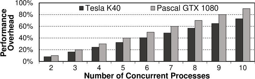
6.1.2 Spatial Multiplexing
Resource utilization can be improved with spatial multiplexing [4], as the ability to execute multiple application kernels concurrently (1) enables the system to co-schedule kernels that have complementary resource demands, and (2) can enable independent progress guarantees for different kernels. Examples of spatial multiplexing support in modern GPUs include (1) application-specific software scheduling of multiple kernels [323]; and (2) NVIDIA’s CUDAstream support [311, 315, 306], which co-schedules kernels from independent “streams” by merging them into a single address space. Unfortunately, these spatial multiplexing mechanisms have significant shortcomings. Software approaches (e.g., Elastic Kernels [323]) require programmers to manually time-slice kernels to enable their mapping onto CUDA streams for concurrency. While CUDAstream supports the flexible partitioning of resources at runtime, merging kernels into a single address space sacrifices memory protection, which is a key requirement in virtualized settings.
True GPU support for multiple concurrent address spaces can address these shortcomings by enabling hardware virtualization. Hardware virtualization allows the system to (1) adapt to changes in application resource utilization or (2) mitigate interference at runtime, by dynamically allocating hardware resources to multiple concurrently-executing applications. NVIDIA and AMD both offer products [159, 9] with partial hardware virtualization support. However, these products simplify memory protection by statically partitioning the hardware resources prior to program execution. As a result, these systems cannot adapt to changes in demand at runtime, and, thus, can still leave GPU resources underutilized. To efficiently support the dynamic sharing of GPU resources, GPUs must provide memory virtualization and memory protection, both of which require efficient mechanisms for virtual-to-physical address translation.
6.2 Baseline Design
We describe (1) the state-of-the-art address translation mechanisms for GPUs, and (2) the overhead of these translation mechanisms when multiple applications share the GPU [343]. We analyze the shortcomings of state-of-the-art address translation mechanisms for GPUs in the presence of multi-application concurrency in Section 6.3, which motivates the need for MASK.
State-of-the-art GPUs extend the GPU memory hierarchy with translation lookaside buffers (TLBs) [343]. TLBs (1) greatly reduce the overhead of address translation by caching recently-used virtual-to-physical address mappings from a page table, and (2) help ensure that memory accesses from application kernels running in different address spaces are isolated from each other. Recent works [343, 342] propose optimized TLB designs that improve address translation performance for GPUs.
We adopt a baseline based on these state-of-the-art TLB designs, whose memory hierarchy makes use of one of two variants for address translation: (1) PWCache, a previously-proposed design that utilizes a shared page walk cache after the L1 TLB [343] (Figure 6.2a); and (2) SharedTLB, a design that utilizes a shared L2 TLB after the L1 TLB (Figure 6.2b). The TLB caches translations that are stored in a multi-level page table (we assume a four-level page table in this work). We extend both TLB designs to handle multi-address-space concurrency. Both variants incorporate private per-core L1 TLBs, and all cores share a highly-threaded page table walker. For PWCache, on a miss in the L1 TLB ( in Figure 6.2a), the GPU initializes a page table walk ( ), which probes the shared page walk cache ( ). Any page walk requests that miss in the page walk cache go to the shared L2 cache and (if needed) main memory. For SharedTLB, on a miss in the L1 TLB ( in Figure 6.2b), the GPU checks whether the translation is available in the shared L2 TLB ( ). If the translation misses in the shared L2 TLB, the GPU initiates a page table walk ( ), whose requests go to the shared L2 cache and (if needed) main memory.222In our evaluation, we use an 8KB page walk cache. The shared L2 TLB is located next to the shared L2 cache. L1 and L2 TLBs use the LRU replacement policy.
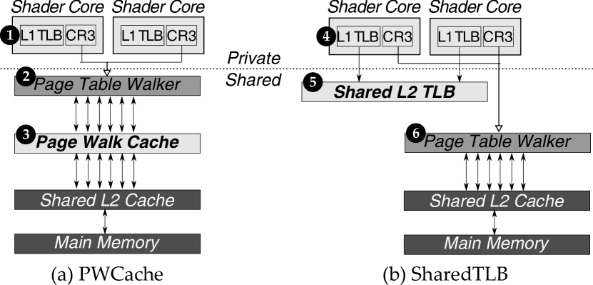
Figure 6.3 compares the performance of both baseline variants (PWCache, depicted in Figure 6.2a, and SharedTLB, depicted in Figure 6.2b), running two separate applications concurrently, to an ideal scenario where every TLB access is a hit (see Table 7.1 for our simulation configuration, and Section 6.5 for our methodology). We find that both variants incur a significant performance overhead (45.0% and 40.6% on average) compared to the ideal case.333We see discrepancies between the performance of our two baseline variants compared to the secs/mask-micro17/results reported by Power et al. [343]. These discrepancies occur because Power et al. assume a much higher L2 data cache access latency (130 ns vs. our 10 ns latency) and a much higher shared L2 TLB access latency (130 ns vs. our 10 ns latency). Our cache latency model, with a 10 ns access latency plus queuing latency (see Table 7.1 in Section 6.5), accurately captures modern GPU parameters [312]. In order to retain the benefits of sharing a GPU across multiple applications, we first analyze the shortcomings of our baseline design, and then use this analysis to develop our new mechanisms that improve TLB performance to make it approach the ideal performance.
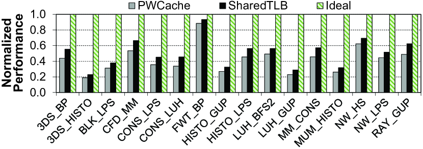
6.3 Design Space Analysis
To improve the performance of address translation in GPUs, we first analyze and characterize the translation overhead in a state-of-the-art baseline (see Section 6.2), taking into account especially the performance challenges induced by multi-address-space concurrency and contention. We first analyze how TLB misses can limit the GPU’s ability to hide long-latency stalls, which directly impacts performance (Section 6.3.1). Next, we discuss two types of memory interference that impact GPU performance: (1) interference introduced by sharing GPU resources among multiple concurrent applications (Section 6.3.2), and (2) interference introduced by sharing the GPU memory hierarchy between address translation requests and data demand requests (Section 6.3.3).
6.3.1 Effect of TLB Misses on GPU Performance
GPU throughput relies on fine-grained multithreading [410, 411, 390, 389] to hide memory latency.444More detailed information about the GPU execution model and its memory hierarchy can be found in [37, 192, 193, 425, 423, 36, 332, 209, 194, 32, 358, 190, 297]. We observe a fundamental tension between address translation and fine-grained multithreading. The need to cache address translations at a page granularity, combined with application-level spatial locality, increase the likelihood that address translations fetched in response to a TLB miss are needed by more than one warp (i.e., many threads). Even with the massive levels of parallelism supported by GPUs, we observe that a small number of outstanding TLB misses can result in the warp scheduler not having enough ready warps to schedule, which in turn limits the GPU’s essential latency-hiding mechanism.
Figure 6.4 illustrates a scenario for an application with four warps, where all four warps execute on the same GPU core. Figure 6.4a shows how the GPU behaves when no virtual-to-physical address translation is required. When Warp A performs a high-latency memory access ( in Figure 6.4), the GPU core does not stall since other warps have schedulable instructions (Warps B–D). In this case, the GPU core selects an active warp (Warp B) in the next cycle ( ), and continues issuing instructions. Even though Warps B–D also perform memory accesses some time later, the accesses are independent of each other, and the GPU avoids stalling by switching to a warp that is not waiting for a memory access ( , ). Figure 6.4b depicts the same 4 warps when address translation is required. Warp A misses in the TLB (indicated in red), and stalls ( ) until the virtual-to-physical translation finishes. In Figure 6.4b, due to spatial locality within the application, the other warps (Warps B–D) need the same address translation as Warp A. As a result, they too stall ( , , ). At this point, the GPU no longer has any warps that it can schedule, and the GPU core stalls until the address translation request completes. Once the address translation request completes ( ), the data demand requests of the warps are issued to memory. Depending on the available memory bandwidth and the parallelism of these data demand requests, the data demand requests from Warps B–D can incur additional queuing latency ( , , ). The GPU core can resume execution only after the data demand request for Warp A is complete ( ).
Three phenomena harm performance in this scenario. First, warps stalled on TLB misses reduce the availability of schedulable warps, which lowers GPU utilization. In Figure 6.4, no available warp exists while the address translation request is pending, so the GPU utilization goes down to 0% for a long time. Second, address translation requests, which are a series of dependent memory requests generated by a page walk, must complete before a pending data demand request that requires the physical address can be issued, which reduces the GPU’s ability to hide latency by keeping many memory requests in flight. Third, when the address translation data becomes available, all stalled warps that were waiting for the translation consecutively execute and send their data demand requests to memory, resulting in additional queuing delay for data demand requests throughout the memory hierarchy.
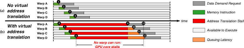
To illustrate how TLB misses significantly reduce the number of ready-to-schedule warps in GPU applications, Figure 6.5 shows the average number of concurrent page table walks (sampled every 10K cycles) for a range of applications, and Figure 6.6 shows the average number of stalled warps per active TLB miss, in the SharedTLB baseline design. Error bars indicate the minimum and maximum values. We observe from Figure 6.5 that more than 20 outstanding TLB misses can perform page walks at the same time, all of which contend for access to address translation structures. From Figure 6.6, we observe that each TLB miss can stall more than 30 warps out of the 64 warps in the core. The combined effect of these observations is that TLB misses in a GPU can quickly stall a large number of warps within a GPU core. The GPU core must wait for the misses to be resolved before issuing data demand requests and resuming execution. Hence, minimizing TLB misses and the page table walk latency is critical.
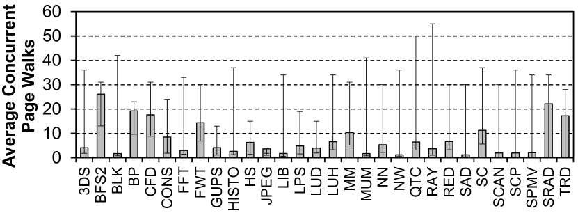

Impact of Large Pages. A large page size can significantly improve the coverage of the TLB [37]. However, a TLB miss on a large page stalls many more warps than a TLB miss on a small page. We find that with a 2MB page size, the average number of stalled warps increases to close to 100% [37], even though the average number of concurrent page table walks never exceeds 5 misses per GPU core. Regardless of the page size, there is a strong need for mechanisms that mitigate the high cost of TLB misses.
6.3.2 Interference at the Shared TLB
When multiple applications are concurrently executed, the address translation overheads discussed in Section 6.3.1 are exacerbated due to inter-address-space interference. To study the impact of this interference, we measure how the TLB miss rates change once another application is introduced. Figure 6.7 compares the 512-entry L2 TLB miss rate of four representative workloads when each application in the workload runs in isolation to the miss rate when the two applications run concurrently and share the L2 TLB. We observe from the figure that inter-address-space interference increases the TLB miss rate significantly for most applications. This occurs because when the applications share the TLB, address translation requests often induce TLB thrashing. The resulting thrashing (1) hurts performance, and (2) leads to unfairness and starvation when applications generate TLB misses at different rates in the TLB (not shown).

6.3.3 Interference Throughout the Memory Hierarchy
Interference at the Shared Data Cache. Prior work [36] demonstrates that while cache hits in GPUs reduce the consumption of off-chip memory bandwidth, the cache hits result in a lower load/store instruction latency only when every thread in the warp hits in the cache. In contrast, when a page table walk hits in the shared L2 cache, the cache hit has the potential to help reduce the latency of other warps that have threads which access the same page in memory. However, TLB-related data can interfere with and displace cache entries housing regular application data, which can hurt the overall GPU performance.
Hence, a trade-off exists between prioritizing address translation requests vs. data demand requests in the GPU memory hierarchy. Based on an empirical analysis of our workloads, we find that translation data from page table levels closer to the page table root are more likely to be shared across warps, and typically hit in the cache. We observe that, for a 4-level page table, the data cache hit rates of address translation requests across all workloads are 99.8%, 98.8%, 68.7%, and 1.0% for the root, first, second, and third levels of the page table, respectively. This means that address translation requests for the deepest page table levels often do not utilize the cache well. Allowing shared structures to cache page table entries from only the page table levels closer to the root could alleviate the interference between low-hit-rate address translation data and regular application data.
Interference at Main Memory. Figure 6.8 characterizes the DRAM bandwidth used by address translation and data demand requests, normalized to the maximum bandwidth available, for our workloads where two applications concurrently share the GPU. Figure 6.9 compares the average latency of address translation requests and data demand requests. We see that even though address translation requests consume only 13.8% of the total utilized DRAM bandwidth (2.4% of the maximum available bandwidth), their average DRAM latency is higher than that of data demand requests. This is undesirable because address translation requests usually stall multiple warps, while data demand requests usually stall only one warp (not shown). The higher latency for address translation requests is caused by the FR-FCFS memory scheduling policy [357, 454], which prioritizes accesses that hit in the row buffer. Data demand requests from GPGPU applications generally have very high row buffer locality [33, 433, 207, 445], so a scheduler that cannot distinguish address translation requests from data demand requests effectively de-prioritizes the address translation requests, increasing their latency, and thus exacerbating the effect on stalled warps.
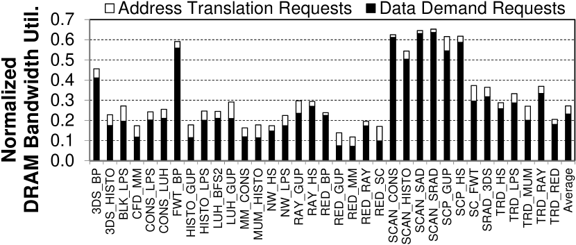

6.3.4 Summary and Our Goal
We make two important observations about address translation in GPUs. First, address translation can greatly hinder a GPU’s ability to hide latency by exploiting thread-level parallelism, since one single TLB miss can stall multiple warps. Second, during concurrent execution, multiple applications generate inter-address-space interference throughout the GPU memory hierarchy, which further increases the TLB miss latency and memory latency. In light of these observations, our goal is to alleviate the address translation overhead in GPUs in three ways: (1) increasing the TLB hit rate by reducing TLB thrashing, (2) decreasing interference between address translation requests and data demand requests in the shared L2 cache, and (3) decreasing the TLB miss latency by prioritizing address translation requests in DRAM without sacrificing DRAM bandwidth utilization.
6.4 Design of MASK
To improve support for multi-application concurrency in state-of-the-art GPUs, we introduce MASK. MASK is a framework that provides memory protection support and employs three mechanisms in the memory hierarchy to reduce address translation overheads while requiring minimal hardware changes, as illustrated in Figure 6.10. First, we introduce TLB-Fill Tokens, which regulate the number of warps that can fill (i.e., insert entries) into the shared TLB in order to reduce TLB thrashing, and utilize a small TLB bypass cache to hold TLB entries from warps that are not allowed to fill the shared TLB due to not having enough tokens ( ). Second, we design an TLB-request-aware L2 Bypass mechanism, which significantly increases the shared L2 data cache utilization and hit rate by reducing interference from the TLB-related data that does not have high temporal locality ( ). Third, we design an Address-space-aware DRAM Scheduler to further reduce interference between address translation requests and data demand requests ( ). In this section, we describe the detailed design and implementation of MASK. We analyze the hardware cost of MASK in Section 6.6.4.
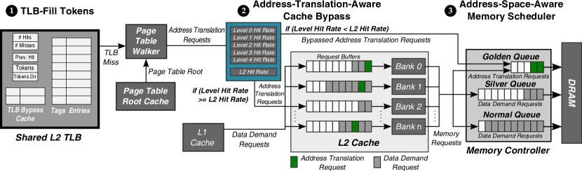
6.4.1 Enforcing Memory Protection
Unlike previously-proposed GPU sharing techniques that do not enable memory protection [191, 430, 311, 251, 315, 409, 129], MASK provides memory protection by allowing different GPU cores to be assigned to different address spaces. MASK uses per-core page table root registers (similar to the CR3 register in x86 systems [173]) to set the current address space on each core. The page table root register value from each GPU core is also stored in a page table root cache for use by the page table walker. If a GPU core’s page table root register value changes, the GPU core conservatively drains all in-flight memory requests in order to ensure correctness. We extend each L2 TLB entry with an address space identifier (ASID). TLB flush operations target a single GPU core, flushing the core’s L1 TLB, and all entries in the L2 TLB that contain the matching address space identifier.
6.4.2 Reducing L2 TLB Interference
Sections 6.3.1 and 6.3.2 demonstrate the need to minimize TLB misses, which induce long-latency stalls. MASK addresses this need with a new mechanism called TLB-Fill Tokens ( in Figure 6.10). To reduce inter-address-space interference at the shared L2 TLB, we use an epoch- and token-based scheme to limit the number of warps from each GPU core that can fill (and therefore contend for) the L2 TLB. While every warp can probe the shared L2 TLB, only warps with tokens can fill the shared L2 TLB. Page table entries (PTEs) requested by warps without tokens are only buffered in a small TLB bypass cache. This token-based mechanism requires two components: (1) a component to determine the number of tokens allocated to each application, and (2) a component that implements a policy for assigning tokens to warps within an application.
When a TLB request arrives at the L2 TLB controller, the GPU probes tags for both the shared L2 TLB and the TLB bypass cache in parallel. A hit in either the TLB or the TLB bypass cache yields a TLB hit.
Determining the Number of Tokens. Every epoch,555We empirically select an epoch length of 100K cycles. MASK tracks (1) the L2 TLB miss rate for each application and (2) the total number of all warps in each core. After the first epoch,666Note that during the first epoch, MASK does not perform TLB bypassing. the initial number of tokens for each application is set to a predetermined fraction of the total number of warps per application.
At the end of any subsequent epoch, for each application, MASK compares the application’s shared L2 TLB miss rate during the current epoch to its miss rate from the previous epoch. If the miss rate increases by more than 2%, this indicates that shared TLB contention is high at the current token count, so MASK decreases the number of tokens allocated to the application. If the miss rate decreases by more than 2%, this indicates that shared TLB contention is low at the current token count, so MASK increases the number of tokens allocated to the application. If the miss rate change is within 2%, the TLB contention has not changed significantly, and the token count remains unchanged.
Assigning Tokens to Warps. Empirically, we observe that (1) the different warps of an application tend to have similar TLB miss rates; and (2) it is beneficial for warps that already have tokens to retain them, as it is likely that their TLB entries are already in the shared L2 TLB. We leverage these two observations to simplify the token assignment logic: our mechanism assigns tokens to warps, one token per warp, in an order based on the warp ID (i.e., if there are tokens, the warps with the lowest warp ID values receive tokens). This simple heuristic is effective at reducing TLB thrashing, as contention at the shared L2 TLB is reduced based on the number of tokens, and highly-used TLB entries that are requested by warps without tokens can still fill the TLB bypass cache and thus still take advantage of locality.
TLB Bypass Cache. While TLB-Fill Tokens can reduce thrashing in the shared L2 TLB, a handful of highly-reused PTEs may be requested by warps with no tokens, which cannot insert the PTEs into the shared L2 TLB. To address this, we add a TLB bypass cache, which is a small 32-entry fully-associative cache. Only warps without tokens can fill the TLB bypass cache in our evaluation. To preserve consistency and correctness, MASK flushes all contents of the TLB and the TLB bypass cache when a PTE is modified. Like the L1 and L2 TLBs, the TLB bypass cache uses the LRU replacement policy.
6.4.3 Minimizing Shared L2 Cache Interference
We find that a TLB miss generates shared L2 cache accesses with varying degrees of locality. Translating addresses through a multi-level page table (e.g., the four-level table used in MASK) can generate dependent memory requests at each level. This causes significant queuing latency at the shared L2 cache, corroborating observations from previous work [36]. Page table entries in levels closer to the root are more likely to be shared and thus reused across threads than entries near the leaves.
To address both interference and queuing delays due to address translation requests at the shared L2 cache, we introduce an TLB-request-aware L2 Bypass mechanism ( in Figure 6.10). To determine which address translation requests should bypass (i.e., skip probing and filling the L2 cache), we leverage our insights from Section 6.3.3. Recall that page table entries closer to the leaves have poor cache hit rates (i.e., the number of cache hits over all cache accesses). We make two observations from our detailed study on the page table hit rates at each page table level (see our technical report [40]). First, not all page table levels have the same hit rate across workloads (e.g., the level 3 hit rate for the MM_CONS workload is only 58.3%, but is 94.5% for RED_RAY). Second, the hit rate behavior can change over time. This means that a scheme that statically bypasses address translation requests for a certain page table level is not effective, as such a scheme cannot adapt to dynamic hit rate behavior changes. Because of the sharp drop-off in the L2 cache hit rate of address translation requests after the first few levels, we can simplify the mechanism to determine when address translation requests should bypass the L2 cache by comparing the L2 cache hit rate of each page table level for address translation requests to the L2 cache hit rate of data demand requests. We impose L2 cache bypassing for address translation requests from a particular page table level when the hit rate of address translation requests to that page table level falls below the hit rate of data demand requests. The shared L2 TLB has counters to track the cache hit rate of each page table level. Each memory request is tagged with a three-bit value that indicates its page walk depth, allowing MASK to differentiate between request types. These bits are set to zero for data demand requests, and to 7 for any depth higher than 6.
6.4.4 Minimizing Interference at Main Memory
There are two types of interference that occur at main memory: (1) data demand requests can interfere with address translation requests, as we saw in Section 6.3.3; and (2) data demand requests from multiple applications can interfere with each other. MASK’s memory controller design mitigates both forms of interference using an Address-space-aware DRAM Scheduler ( in Figure 6.10).
The Address-space-aware DRAM Scheduler breaks the traditional DRAM request buffer into three separate queues. The first queue, called the Golden Queue, is a small FIFO queue.777We observe that address translation requests have low row buffer locality. Thus, there is no significant performance benefit if the memory controller reorders address translation requests within the Golden Queue to exploit row buffer locality. Address translation requests always go to the Golden Queue, while data demand requests go to one of the two other queues (the size of each queue is similar to the size of a typical DRAM request buffer). The second queue, called the Silver Queue, contains data demand requests from one selected application. The last queue, called the Normal Queue, contains data demand requests from all other applications. The Golden Queue is used to prioritize TLB misses over data demand requests. The Silver Queue allows the GPU to (1) avoid starvation when one or more applications hog memory bandwidth, and (2) improve fairness when multiple applications execute concurrently [281, 33]. When one application unfairly hogs DRAM bandwidth in the Normal Queue, the Silver Queue can process data demand requests from another application that would otherwise be starved or unfairly delayed.
Our Address-space-aware DRAM Scheduler always prioritizes requests in the Golden Queue over requests in the Silver Queue, which are always prioritized over requests in the Normal Queue. To provide higher priority to applications that are likely to be stalled due to concurrent TLB misses, and to minimize the time that bandwidth-heavy applications have access to the silver queue, each application takes turns being assigned to the Silver Queue based on two per-application metrics: (1) the number of concurrent page walks, and (2) the number of warps stalled per active TLB miss. The number of data demand requests each application can add to the Silver Queue, when the application gets its turn, is shown as in Equation 6.1. After application () reaches its quota, the next application () is then allowed to send its requests to the Silver Queue, and so on. Within both the Silver Queue and Normal Queue, FR-FCFS [357, 454] is used to schedule requests.
| (6.1) |
To track the number of outstanding concurrent page walks ( in Equation 6.1), we add a 6-bit counter per application to the shared L2 TLB.888We leave techniques to virtualize this counter for more than 64 applications as future work. This counter tracks the number of concurrent TLB misses. To track the number of warps stalled per active TLB miss ( in Equation 6.1), we add a 6-bit counter to each TLB MSHR entry, which tracks the maximum number of warps that hit in the entry. The Address-space-aware DRAM Scheduler resets all of these counters every epoch (see Section 6.4.2).
We find that the number of concurrent address translation requests that go to each memory channel is small, so our design has an additional benefit of lowering the page table walk latency (because it prioritizes address translation requests) while minimizing interference.
6.4.5 Page Faults and TLB Shootdowns
Address translation inevitably introduces page faults. Our design can be extended to use techniques from previous works, such as performing copy-on-write for handling page faults [343], and either exception support [272] or demand paging techniques [453, 315, 14] for major faults. We leave this as future work.
6.5 Methodology
To evaluate MASK, we model the NVIDIA Maxwell architecture [312], and the TLB-fill bypassing, cache bypassing, and memory scheduling mechanisms in MASK, using the Mosaic simulator [37], which is based on GPGPU-Sim 3.2.2 [46]. We heavily modify the simulator to accurately model the behavior of CUDA Unified Virtual Addressing [312, 315] as described below. Table 7.1 provides the details of our baseline GPU configuration. Our baseline uses the FR-FCFS memory scheduling policy [357, 454], based on findings from previous works [33, 445, 73] which show that FR-FCFS provides good performance for GPGPU applications compared to other, more sophisticated schedulers [220, 221]. We have open-sourced our modified simulator online [366].
| GPU Core Configuration | |
|---|---|
| System Overview | 30 cores, 64 execution units per core. |
| Shader Core | 1020 MHz, 9-stage pipeline, 64 threads per warp, |
| GTO scheduler [359]. | |
| Page Table Walker | Shared page table walker, traversing 4-level page tables. |
| Cache and Memory Configuration | |
| Private L1 Cache | 16KB, 4-way associative, LRU, L1 misses are |
| coalesced before accessing L2, 1-cycle latency. | |
| Private L1 TLB | 64 entries per core, fully associative, LRU, 1-cycle latency. |
| Shared L2 Cache | 2MB total, 16-way associative, LRU, 16 cache banks, |
| 2 ports per cache bank, 10-cycle latency | |
| Shared L2 TLB | 512 entries total, 16-way associative, LRU, 2 ports, |
| 10-cycle latency | |
| Page Walk Cache | 16-way 8KB, 10-cycle latency |
| DRAM | GDDR5 1674 MHz [170], 8 channels, 8 banks per rank, 1 rank, |
| FR-FCFS scheduler [357, 454], burst length 8 | |
TLB and Page Table Walker Model. We accurately model both TLB design variants discussed in Section 6.2. We employ the non-blocking TLB implementation used by Pichai et al. [342]. Each core has a private L1 TLB. The page table walker is shared across threads, and admits up to 64 concurrent threads for walks. On a TLB miss, a page table walker generates a series of dependent requests that probe the L2 cache and main memory as needed. We faithfully model the multi-level page walks.
Workloads. We randomly select 27 applications from the CUDA SDK [309], Rodinia [77], Parboil [396], LULESH [203, 204], and SHOC [90] suites. We classify these benchmarks based on their L1 and L2 TLB miss rates into one of four groups, as shown in Table 6.2. For our multi-application secs/mask-micro17/results, we randomly select 35 pairs of applications, avoiding pairs where both applications have a low L1 TLB miss rate (i.e., 20%) and low L2 TLB miss rate (i.e., 20%), since these applications are relatively insensitive to address translation overheads. The application that finishes first is relaunched to keep the GPU core busy and maintain memory contention.
| L1 TLB Miss Rate | L2 TLB Miss Rate | Benchmark Name |
| Low | Low | LUD, NN |
| Low | High | BFS2, FFT, HISTO, NW, |
| QTC, RAY, SAD, SCP | ||
| High | Low | BP, GUP, HS, LPS |
| High | High | 3DS, BLK, CFD, CONS, |
| FWT, LUH, MM, MUM, RED, SC, | ||
| SCAN, SRAD, TRD |
We divide 35 application-pairs into three workload categories based on the number of applications that have both high L1 and L2 TLB miss rates, as high TLB miss rates at both levels indicate a high amount of pressure on the limited TLB resources. n-HMR contains application-pairs where n applications in the workload have both high L1 and L2 TLB miss rates.
Evaluation Metrics. We report performance using weighted speedup [107, 108], a commonly-used metric to evaluate the performance of a multi-application workload [33, 209, 221, 220, 293, 292, 287, 94, 93, 402, 401, 417]. Weighted speedup is defined as , where is the IPC of an application that runs on the same number of GPU cores, but does not share GPU resources with any other application, and is the IPC of an application when it runs concurrently with other applications. We report the unfairness of each design using maximum slowdown, defined as [104, 33, 93, 220, 221, 418, 398, 400, 402, 401, 417].
Scheduling and Partitioning of Cores. We assume an oracle GPU scheduler that finds the best partitioning of the GPU cores for each pair of applications. For each pair of applications that are concurrently executed, the scheduler partitions the cores according to the best weighted speedup for that pair found by an exhaustive search over all possible static core partitionings. Neither the L2 cache nor main memory are partitioned. All applications can use all of the shared L2 cache and the main memory.
Design Parameters. MASK exposes two configurable parameters: for TLB-Fill Tokens, and for the Address-space-aware DRAM Scheduler. A sweep over the range of possible values reveals less than 1% performance variance, as TLB-Fill Tokens are effective at reconfiguring the total number of tokens to a steady-state value (Section 6.4.2). In our evaluation, we set to 80%. We set to empirically.
6.6 Evaluation
We compare the performance of MASK against four GPU designs. The first, called Static, uses a static spatial partitioning of resources, where an oracle is used to partition GPU cores, but the shared L2 cache and memory channels are partitioned equally across applications. This design is intended to capture key design aspects of NVIDIA GRID [159] and AMD FirePro [9], based on publicly-available information. The second design, called PWCache, models the page walk cache baseline design we discuss in Section 6.2. The third design, called SharedTLB, models the shared L2 TLB baseline design we discuss in Section 6.2. The fourth design, Ideal, represents a hypothetical GPU where every single TLB access is a TLB hit. In addition to these designs, we report the performance of the individual components of MASK: TLB-Fill Tokens (MASK-TLB), TLB-request-aware L2 Bypass (MASK-Cache), and Address-space-aware DRAM Scheduler (MASK-DRAM).
6.6.1 Multiprogrammed Performance
Figure 6.11 compares the average performance by workload category of Static, PWCache, SharedTLB, and Ideal to MASK and the three individual components of MASK. We make two observations from Figure 6.11. First, compared to SharedTLB, which is the best-performing baseline, MASK improves the weighted speedup by 57.8% on average. Second, we find that MASK performs only 23.2% worse than Ideal (where all accesses to the L1 TLB are hits). This demonstrates that MASK reduces a large portion of the TLB miss overhead.
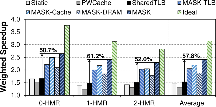
Individual Workload Performance. Figures 6.14, 6.14, and 6.14 compare the weighted speedup of each individual multiprogrammed workload for MASK, and the individual performance of its three components (MASK-TLB, MASK-Cache, and MASK-DRAM), against Static, PWCache, and SharedTLB for the 0-HMR (Figure 6.14), 1-HMR (Figure 6.14), and 2-HMR (Figure 6.14) workload categories. Each group of bars in Figures 6.14–6.14 represents a pair of co-scheduled benchmarks. We make two observations from the figures. First, compared to Static, where resources are statically partitioned, MASK provides better performance, because when an application stalls for concurrent TLB misses, it no longer needs a large amount of other shared resources, such as DRAM bandwidth. During such stalls, other applications can utilize these resources. When multiple GPGPU applications run concurrently using MASK, TLB misses from two or more applications can be staggered, increasing the likelihood that there will be heterogeneous and complementary resource demands. Second, MASK provides significant performance improvements over both PWCache and SharedTLB regardless of the workload type (i.e., 0-HMR to 2-HMR). This indicates that MASK is effective at reducing the address translation overhead both when TLB contention is high and when TLB contention is relatively low.


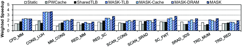
Our technical report [40] provides additional analysis on the aggregate throughput (system-wide IPC). In the report, we show that MASK provides 43.4% better aggregate throughput compared to SharedTLB.
Figure 6.15 compares the unfairness of MASK to that of Static, PWCache, and SharedTLB. We make two observations. First, compared to statically partitioning resources (Static), MASK provides better fairness by allowing both applications to access all shared resources. Second, compared to SharedTLB, which is the baseline that provides the best fairness, MASK reduces unfairness by 22.4% on average. As the number of tokens for each application changes based on the L2 TLB miss rate, applications that benefit more from the shared L2 TLB are more likely to get more tokens, causing applications that do not benefit from shared L2 TLB space to yield that shared L2 TLB space to other applications. Our application-aware token distribution mechanism and TLB-fill bypassing mechanism work in tandem to reduce the amount of shared L2 TLB thrashing observed in Section 6.3.2.
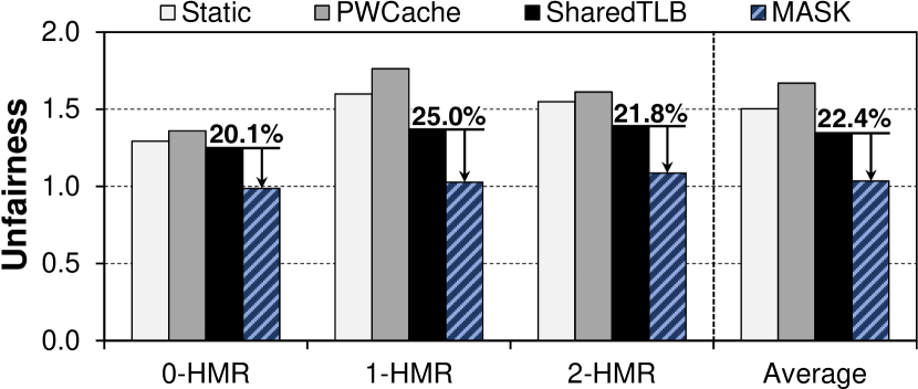
Individual Application Analysis. MASK provides better throughput for all individual applications sharing the GPU due to reduced TLB miss rates for each application (shown in our technical report [40]). The per-application L2 TLB miss rates are reduced by over 50% on average, which is in line with the reduction in system-wide L2 TLB miss rates (see Section 6.6.2). Reducing the number of TLB misses via our TLB-fill bypassing policy (Section 6.4.2), and reducing the latency of TLB misses via our shared L2 bypassing (Section 6.4.3) and TLB- and application-aware DRAM scheduling (Section 6.4.4) policies, enables significant performance improvement.
In some cases, running two applications concurrently provides better performance as well as lower unfairness than running each application alone (e.g., for the RED_BP and RED_RAY workloads in Figure 6.14, and the SC_FWT workload in Figure 6.14). We attribute such cases to substantial improvements (more than 10%) of two factors: a lower L2 cache queuing latency for bypassed address translation requests, and a higher L1 cache hit rate of data demand requests when applications share the L2 cache and main memory with other applications.
We conclude that MASK is effective at reducing the address translation overheads in modern GPUs, and thus at improving both performance and fairness, by introducing address translation request awareness throughout the GPU memory hierarchy.
6.6.2 Component-by-Component Analysis
This section characterizes MASK’s underlying mechanisms (MASK-TLB, MASK-Cache, and MASK-DRAM). Figure 6.11 shows the average performance improvement of each individual component of MASK compared to Static, PWCache, SharedTLB, and MASK. We summarize our key findings here, and provide a more detailed analysis in our technical report [40].
Effectiveness of TLB-Fill Tokens. MASK uses TLB-Fill Tokens to reduce thrashing. We compare TLB hit rates for Static, SharedTLB, and MASK-TLB. The hit rates for Static and SharedTLB are substantially similar. MASK-TLB increases shared L2 TLB hit rates by 49.9% on average over SharedTLB [40], because the TLB-Fill Tokens mechanism reduces the number of warps utilizing the shared L2 TLB entries, in turn reducing the miss rate. The TLB bypass cache stores frequently-used TLB entries that cannot be filled in the traditional TLB. Measurement of the average TLB bypass cache hit rate (66.5%) confirms this conclusion [40].999We find that the performance of MASK-TLB saturates when we increase the TLB bypass cache beyond 32 entries for the workloads that we evaluate.
Effectiveness of TLB-request-aware L2 Bypass. MASK uses TLB-request-aware L2 Bypass with the goal of prioritizing address translation requests. We measure the average L2 cache hit rate for address translation requests. We find that for address translation requests that fill into the shared L2 cache, TLB-request-aware L2 Bypass is very effective at selecting which blocks to cache, resulting in an address translation request hit rate that is higher than 99% for all of our workloads. At the same time, TLB-request-aware L2 Bypass minimizes the impact of long L2 cache queuing latency [36], leading to a 43.6% performance improvement compared to SharedTLB (as shown in Figure 6.11).
Effectiveness of Address-space-aware DRAM Scheduler. To characterize the performance impact of MASK’s DRAM scheduler, we compare the DRAM bandwidth utilization and average DRAM latency of (1) address translation requests and (2) data demand requests for the baseline designs and MASK, and make two observations. First, we find that MASK is effective at reducing the DRAM latency of address translation requests, which contributes to the 22.7% performance improvement of MASK-DRAM over SharedTLB, as shown in Figure 6.11. In cases where the DRAM latency is high, our DRAM scheduling policy reduces the latency of address translation requests by up to 10.6% (SCAN_SAD), while increasing DRAM bandwidth utilization by up to 5.6% (SCAN_HISTO). Second, we find that when an application is suffering severely from interference due to another concurrently-executing application, the Silver Queue significantly reduces the latency of data demand requests from the suffering application. For example, when the Silver Queue is employed, SRAD from the SCAN_SRAD application-pair performs 18.7% better, while both SCAN and CONS from SCAN_CONS perform 8.9% and 30.2% better, respectively. Our technical report [40] provides a more detailed analysis of the impact of our Address-space-aware DRAM Scheduler.
We conclude that each component of MASK provides complementary performance improvements by introducing address-translation-aware policies at different memory hierarchy levels.
6.6.3 Scalability and Generality
This section evaluates the scalability of MASK and provides evidence that the design generalizes well across different architectures. We summarize our key findings here, and provide a more detailed analysis in our technical report [40].
Scalability. We compare the performance of SharedTLB, which is the best-performing state-of-the-art baseline design, and MASK, normalized to Ideal performance, as the number of concurrently-running applications increases from one to five. In general, as the application count increases, contention for shared resources (e.g., shared L2 TLB, shared L2 cache) draws the performance for both SharedTLB and MASK further from the performance of Ideal. However, MASK maintains a consistent performance advantage relative to SharedTLB, as shown in Table 6.3. The performance gain of MASK relative to SharedTLB is more pronounced at higher levels of multi-application concurrency because (1) the shared L2 TLB becomes heavily contended as the number of concurrent applications increases, and (2) MASK is effective at reducing the amount of contention at the heavily-contended shared TLB.
| Number of Applications | 1 | 2 | 3 | 4 | 5 |
|---|---|---|---|---|---|
| SharedTLB performance | 47.1% | 48.7% | 38.8% | 34.2% | 33.1% |
| normalized to Ideal | |||||
| MASK performance | 68.5% | 76.8% | 62.3% | 55.0% | 52.9% |
| normalized to Ideal |
Generality. MASK is an architecture-independent design: our techniques are applicable to any SIMT machine [310, 311, 312, 315, 7, 8, 427, 278, 344]. To demonstrate this, we evaluate our two baseline variants (PWCache and SharedTLB) and MASK on two additional GPU architectures: the GTX480 (Fermi architecture [310]), and an integrated GPU architecture [343, 5, 432, 61, 179, 80, 181, 344, 278, 307, 308], as shown in Table 6.4. We make three key conclusions. First, address translation leads to significant performance overhead in both PWCache and SharedTLB. Second, MASK provides a 46.9% average performance improvement over PWCache and a 29.1% average performance improvement over SharedTLB on the Fermi architecture, getting to within 22% of the performance of Ideal. Third, on the integrated GPU configuration used in previous work [343], we find that MASK provides a 23.8% performance improvement over PWCache and a 68.8% performance improvement over SharedTLB, and gets within 35.5% of the performance of Ideal.
| Relative Performance | Fermi | Integrated GPU [343] |
|---|---|---|
| PWCache | 53.1% | 52.1% |
| SharedTLB | 60.4% | 38.2% |
| MASK | 78.0% | 64.5% |
We conclude that MASK is effective at (1) reducing the performance overhead of address translation, and (2) significantly improving system performance over both the PWCache and SharedTLB designs, regardless of the GPU architecture.
Sensitivity to L1 and L2 TLB Sizes. We evaluate the benefit of MASK over many different TLB sizes in our technical report [40]. We make two observations. First, MASK is effective at reducing (1) TLB thrashing at the shared L2 TLB, and (2) the latency of address translation requests regardless of TLB size. Second, as we increase the shared L2 TLB size from 64 to 8192 entries, MASK outperforms SharedTLB for all TLB sizes except the 8192-entry shared L2 TLB. At 8192 entries, MASK and SharedTLB perform equally, because the working set fits completely within the 8192-entry shared L2 TLB.
Sensitivity to Memory Policies. We study the sensitivity of MASK to (1) main memory row policy, and (2) memory scheduling policies. We find that for all of our baselines and for MASK, performance with an open-row policy [220] is similar (within 0.8%) to the performance with a closed-row policy, which is used in various CPUs [178, 175, 181]. Aside from the FR-FCFS scheduler [357, 454], we use MASK in conjunction with another state-of-the-art GPU memory scheduler [191], and find that with this scheduler, MASK improves performance by 44.2% over SharedTLB. We conclude that MASK is effective across different memory policies.
Sensitivity to Different Page Sizes. We evaluate the performance of MASK with 2MB large pages assuming an ideal page fault latency [40, 32] (not shown). We provide two observations. First, even with the larger page size, SharedTLB continues to experience high contention during address translation, causing its average performance to fall 44.5% short of Ideal. Second, we find that using MASK allows the GPU to perform within 1.8% of Ideal.
6.6.4 Hardware Overheads
To support memory protection, each L2 TLB entry has an 9-bit address space identifier (ASID), which translates to an overhead of 7% of the L2 TLB size in total.
At each core, our TLB-Fill Tokens mechanism uses (1) two 16-bit counters to track the shared L2 TLB hit rate, with one counter tracking the number of shared L2 TLB hits, and the other counter tracking the number of shared L2 TLB misses; (2) a 256-bit vector addressable by warp ID to track the number of active warps, where each bit is set when a warp uses the shader core for the first time, and is reset every epoch; and (3) an 8-bit incrementer that tracks the total number of unique warps executed by the core (i.e., its counter value is incremented each time a bit is set in the bit vector).
We augment the shared cache with a 32-entry fully-associative content addressable memory (CAM) for the bypass cache, 30 15-bit token counters, and 30 1-bit direction registers to record whether the token count increased or decreased during the previous epoch. These structures allow the GPU to distribute tokens among up to 30 concurrent applications. In total, we add 706 bytes of storage (13 bytes per core in the L1 TLB, and 316 bytes total in the shared L2 TLB), which adds 1.6% to the baseline L1 TLB size and 3.8% to the baseline L2 TLB size (in addition to the 7% overhead due to the ASID bits).
TLB-request-aware L2 Bypass uses ten 8-byte counters per core to track L2 cache hits and L2 cache accesses per level. The resulting 80 bytes add less than 0.1% to the baseline shared L2 cache size. Each L2 cache and memory request requires an additional 3 bits to specify the page walk level, as we discuss in Section 6.4.3.
For each memory channel, our Address-space-aware DRAM Scheduler contains a 16-entry FIFO queue for the Golden Queue, a 64-entry memory request buffer for the Silver Queue, and a 192-entry memory request buffer for the Normal Queue. This adds an extra 6% of storage overhead to the DRAM request queue per memory controller.
Area and Power Consumption. We compare the area and power consumption of MASK to PWCache and SharedTLB using CACTI [288]. PWCache and SharedTLB have near-identical area and power consumption, as we size the page walk cache and shared L2 TLB (see Section 6.2) such that they both use the same total area. We find that MASK introduces a negligible overhead to both baselines, consuming less than 0.1% additional area and 0.01% additional power in each baseline. We provide a detailed analysis of area and power consumption in our technical report [40].
6.7 MASK: Conclusion
Spatial multiplexing support, which allows multiple applications to run concurrently, is needed to efficiently deploy GPUs in a large-scale computing environment. Unfortunately, due to the primitive existing support for memory virtualization, many of the performance benefits of spatial multiplexing are lost in state-of-the-art GPUs. We perform a detailed analysis of state-of-the-art mechanisms for memory virtualization, and find that current address translation mechanisms (1) are highly susceptible to interference across the different address spaces of applications in the shared TLB structures, which leads to a high number of page table walks; and (2) undermine the fundamental latency-hiding techniques of GPUs, by often stalling hundreds of threads at once. To alleviate these problems, we propose MASK, a new memory hierarchy designed carefully to support multi-application concurrency at low overhead. MASK consists of three major components in different parts of the memory hierarchy, all of which incorporate address translation request awareness. These three components work together to lower inter-application interference during address translation, and improve L2 cache utilization and memory latency for address translation requests. MASK improves performance by 57.8%, on average across a wide range of multiprogrammed workloads, over the state-of-the-art. We conclude that MASK provides a promising and effective substrate for multi-application execution on GPUs, and hope future work builds on the mechanism we provide and open source [366].
Chapter 7 Reducing Inter-address-space Interference with Mosaic
Graphics Processing Units (GPUs) are used for an ever-growing range of application domains due to steady increases in GPU compute density and continued improvements in programming tools [313, 216, 12]. The growing adoption of GPUs has in part been due to better high-level language support [313, 363, 403, 66], which has improved GPU programmability. Recent support within GPUs for memory virtualization features, such as a unified virtual address space [310, 12], demand paging [315], and preemption [315, 9], can provide fundamental improvements that can ease programming. These features allow developers to exploit key benefits that have long been taken for granted in CPUs (e.g., application portability, multi-application execution). Such familiar features can dramatically improve programmer productivity and further boost GPU adoption. However, a number of challenges have kept GPU memory virtualization from achieving performance similar to that in CPUs [420, 269]. In this work, we focus on two fundamental challenges: (1) the address translation challenge, and (2) the demand paging challenge.
Address Translation Challenge. Memory virtualization relies on page tables to store virtual-to-physical address translations. Conventionally, systems store one translation for every base page (e.g., a 4KB page). To translate a virtual address on demand, a series of serialized memory accesses are required to traverse (i.e., walk) the page table [343, 342]. These serialized accesses clash with the single-instruction multiple-thread (SIMT) execution model [297, 251, 120] used by GPU-based systems, which relies on high degrees of concurrency through thread-level parallelism (TLP) to hide long memory latencies during GPU execution. Translation lookaside buffers (TLBs) can reduce the latency of address translation by caching recently-used address translation information. Unfortunately, as application working sets and DRAM capacity have increased in recent years, state-of-the-art GPU TLB designs [343, 342] suffer due to inter-application interference and stagnant TLB sizes. Consequently, GPUs have poor TLB reach, i.e., the TLB covers only a small fraction of the physical memory working set of an application. Poor TLB reach is particularly detrimental with the SIMT execution model, as a single TLB miss can stall hundreds of threads at once, undermining TLP within a GPU and significantly reducing performance [420, 269].
Large pages (e.g., the 2MB or 1GB pages in modern CPUs [179, 181]) can significantly reduce the overhead of address translation. A major constraint for TLB reach is the small, fixed number of translations that a TLB can hold. If we store one translation for every large page instead of one translation for every base page, the TLB can cover a much larger fraction of the virtual address space using the same number of page translation entries. Large pages have been supported by CPUs for decades [381, 387], and large page support is emerging for GPUs [343, 453, 342]. However, large pages increase the risk of internal fragmentation, where a portion of the large page is unallocated (or unused). Internal fragmentation occurs because it is often difficult for an application to completely utilize large contiguous regions of memory. This fragmentation leads to (1) memory bloat, where a much greater amount of physical memory is allocated than the amount of memory that the application needs; and (2) longer memory access latencies, due to a lower effective TLB reach and more page faults [228].
Demand Paging Challenge. For discrete GPUs (i.e., GPUs that are not in the same package/die as the CPU), demand paging can incur significant overhead. With demand paging, an application can request data that is not currently resident in GPU memory. This triggers a page fault, which requires a long-latency data transfer for an entire page over the system I/O bus, which, in today’s systems, is also called the PCIe bus [331]. A single page fault can cause multiple threads to stall at once, as threads often access data in the same page due to data locality. As a result, the page fault can significantly reduce the amount of TLP that the GPU can exploit, and the long latency of a page fault harms performance [453].
Unlike address translation, which benefits from larger pages, demand paging benefits from smaller pages. Demand paging for large pages requires a greater amount of data to be transferred over the system I/O bus during a page fault than for conventional base pages. The larger data transfer size increases the transfer time significantly, due to the long latency and limited bandwidth of the system I/O bus. This, in turn, significantly increases the amount of time that GPU threads stall, and can further decrease the amount of TLP. To make matters worse, as the size of a page increases, there is a greater probability that an application does not need all of the data in the page. As a result, threads may stall for a longer time without gaining any further benefit in return.
Page Size Trade-Off. We find that memory virtualization in state-of-the-art GPU systems has a fundamental trade-off due to the page size choice. A larger page size reduces address translation stalls by increasing TLB reach and reducing the number of high-latency TLB misses. In contrast, a smaller page size reduces demand paging stalls by decreasing the amount of unnecessary data transferred over the system I/O bus [343, 453]. We can relax the page size trade-off by using multiple page sizes transparently to the application, and, thus, to the programmer. In a system that supports multiple page sizes, several base pages that are contiguous in both virtual and physical memory can be coalesced (i.e., combined) into a single large page, and a large page can be splintered (i.e., split) into multiple base pages. With multiple page sizes, and the ability to change virtual-to-physical mappings dynamically, the GPU system can support good TLB reach by using large pages for address translation, while providing better demand paging performance by using base pages for data transfer.
Application-transparent support for multiple page sizes has proven challenging for CPUs [228, 298]. A key property of memory virtualization is to enforce memory protection, where a distinct virtual address space (i.e., a memory protection domain) is allocated to an individual application or a virtual machine, and memory is shared safely (i.e., only with explicit permissions for accesses across different address spaces). In order to ensure that memory protection guarantees are not violated, coalescing operations can combine contiguous physical base pages into a single physical large page only if all base pages belong to the same virtual address space.
Unfortunately, in both CPU and state-of-the-art GPU memory managers, existing memory access patterns and allocation mechanisms make it difficult to find regions of physical memory where base pages can be coalesced. We show an example of this in Figure 7.1a, which illustrates how a state-of-the-art GPU memory manager [343] allocates memory for two applications. Within a single large page frame (i.e., a contiguous piece of physical memory that is the size of a large page and whose starting address is page aligned), the GPU memory manager allocates base pages from both Applications 1 and 2 ( in the figure). As a result, the memory manager cannot coalesce the base pages into a large page ( ) without first migrating some of the base pages, which would incur a high latency.

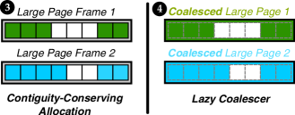
We make a key observation about the memory behavior of contemporary general-purpose GPU (GPGPU) applications. The vast majority of memory allocations in GPGPU applications are performed en masse (i.e., a large number of pages are allocated at the same time). The en masse memory allocation presents us with an opportunity: with so many pages being allocated at once, we can rearrange how we allocate the base pages to ensure that (1) all of the base pages allocated within a large page frame belong to the same virtual address space, and (2) base pages that are contiguous in virtual memory are allocated to a contiguous portion of physical memory and aligned within the large page frame. Our goal in this work is to develop an application-transparent memory manager that performs such memory allocation, and uses this allocation property to efficiently support multiple page sizes in order to improve TLB reach and efficiently support demand paging.
To this end, we present Mosaic, a new GPU memory manager that uses our key observation to provide application-transparent support for multiple page sizes in GPUs while avoiding high overhead for coalescing and splintering pages. The key idea of Mosaic is to (1) transfer data to GPU memory at the small base page (e.g., 4KB) granularity, (2) allocate physical base pages in a way that avoids the need to migrate data during coalescing, and (3) use a simple coalescing mechanism to combine base pages into large pages (e.g., 2MB) and thus increase TLB reach. Figure 7.1b shows a high-level overview of how Mosaic allocates and coalesces pages. Mosaic consists of three key design components: (1) Contiguity-conserving Allocation (CocoA), a memory allocator which provides a soft guarantee that all of the base pages within the same large page range belong to only a single application ( in the figure); (2) Lazy-Coalescer, a page size selection mechanism that merges base pages into a large page immediately after allocation ( ), and thus does not need to monitor base pages to make coalescing decisions or migrate base pages; and (3) Contiguity-aware Compaction (CaC), a memory compaction mechanism that transparently migrates data to avoid internal fragmentation within a large page frame, which frees up large page frames for CocoA.
Key Results. We evaluate Mosaic using 235 workloads. Each workload consists of multiple GPGPU applications from a wide range of benchmark suites. Our evaluations show that compared to a contemporary GPU that uses only 4KB base pages, a GPU with Mosaic reduces address translation overheads while efficiently achieving the benefits of demand paging, thanks to its use of multiple page sizes. When we compare to a GPU with a state-of-the-art memory manager (see Section 7.2.1), we find that a GPU with Mosaic provides an average speedup of 55.5% and 29.7% for homogeneous and heterogeneous multi-application workloads, respectively, and comes within 6.8% and 15.4% of the performance of a GPU with an ideal TLB, where all TLB requests are hits. Thus, by alleviating the page size trade-off between address translation and demand paging overhead, Mosaic improves the efficiency and practicality of multi-application execution on the GPU.
This chapter makes the following contributions:
-
•
We analyze fundamental trade-offs on choosing the correct page size to optimize both address translation (which benefits from larger pages) and demand paging (which benefits from smaller pages). Based on our analyses, we motivate the need for application-transparent support of multiple page sizes in a GPU.
-
•
We present Mosaic, a new GPU memory manager that efficiently supports multiple page sizes. Mosaic uses a novel mechanism to allocate contiguous virtual pages to contiguous physical pages in the GPU memory, and exploits this property to coalesce contiguously-allocated base pages into a large page for address translation with low overhead and no data migration, while still using base pages during demand paging.
-
•
We show that Mosaic’s application-transparent support for multiple page sizes effectively improves TLB reach while efficiently achieving the benefits of demand paging. Overall, Mosaic improves the average performance of homogeneous and heterogeneous multi-application workloads by 55.5% and 29.7%, respectively, over a state-of-the-art GPU memory manager.
7.1 Background
We first provide necessary background on contemporary GPU architectures. In Section 7.1.1, we discuss the GPU execution model. In Section 7.1.2, we discuss state-of-the-art support for GPU memory virtualization.
7.1.1 GPU Execution Model
GPU applications use fine-grained multithreading [410, 411, 390, 389]. A GPU application is made up of thousands of threads. These threads are clustered into thread blocks (also known as work groups), where each thread block consists of multiple smaller bundles of threads that execute concurrently. Each such thread bundle is known as a warp, or a wavefront. Each thread within the warp executes the same instruction at the same program counter value. The GPU avoids stalls due to dependencies and long memory latencies by taking advantage of thread-level parallelism (TLP), where the GPU swaps out warps that have dependencies or are waiting on memory with other warps that are ready to execute.
A GPU consists of multiple streaming multiprocessors (SMs), also known as shader cores. Each SM executes one warp at a time using the single-instruction, multiple-thread (SIMT) execution model [297, 251, 120]. Under SIMT, all of the threads within a warp are executed in lockstep. Due to lockstep execution, a warp stalls when any one thread within the warp has to stall. This means that a warp is unable to proceed to the next instruction until the slowest thread in the warp completes the current instruction.
The GPU memory hierarchy typically consists of multiple levels of memory. In contemporary GPU architectures, each SM has a private data cache, and has access to one or more shared memory partitions through an interconnect (typically a crossbar). A memory partition combines a single slice of the banked L2 cache with a memory controller that connects the GPU to off-chip main memory (DRAM). More detailed information about the GPU memory hierarchy can be found in [192, 193, 425, 423, 36, 332, 209, 194, 32, 358, 190].
7.1.2 Virtualization Support in GPUs
Hardware-supported memory virtualization relies on address translation to map each virtual memory address to a physical address within the GPU memory. Address translation uses page-granularity virtual-to-physical mappings that are stored within a multi-level page table. To look up a mapping within the page table, the GPU performs a page table walk, where a page table walker traverses through each level of the page table in main memory until the walker locates the page table entry for the requested mapping in the last level of the table. GPUs with virtual memory support have translation lookaside buffers (TLBs), which cache page table entries and avoid the need to perform a page table walk for the cached entries, thus reducing the address translation latency.
The introduction of address translation hardware into the GPU memory hierarchy puts TLB misses on the critical path of application execution, as a TLB miss invokes a page table walk that can stall multiple threads and degrade performance significantly. (We study the impact of TLB misses and page table walks in Section 7.2.1.) A GPU uses multiple TLB levels to reduce the number of TLB misses, typically including private per-SM L1 TLBs and a shared L2 TLB [453, 342, 343]. Traditional address translation mechanisms perform memory mapping using a base page size of 4KB. Prior work for integrated GPUs (i.e., GPUs that are in the same package or die as the CPU) has found that using a larger page size can improve address translation performance by improving TLB reach (i.e., the maximum fraction of memory that can be accessed using the cached TLB entries) [453, 342, 343]. For a TLB that holds a fixed number of page table entries, using the large page (e.g., a page with a size of 2MB or greater) as the granularity for mapping greatly increases the TLB reach, and thus reduces the TLB miss rate, compared to using the base page granularity. While memory hierarchy designs for widely-used GPU architectures from NVIDIA, AMD, and Intel are not publicly available, it is widely accepted that contemporary GPUs support TLB-based address translation and, in some models, large page sizes [9, 310, 311, 312, 269]. To simplify translation hardware in a GPU that uses multiple page sizes (i.e., both base pages and large pages), we assume that each TLB level contains two separate sets of entries [201, 122, 202, 340, 341, 325], where one set of entries stores only base page translations, while the other set of entries stores only large page translations.
State-of-the-art GPU memory virtualization provides support for demand paging [343, 453, 14, 12, 315]. In demand paging, all of the memory used by a GPU application does not need to be transferred to the GPU memory at the beginning of application execution. Instead, during application execution, when a GPU thread issues a memory request to a page that has not yet been allocated in the GPU memory, the GPU issues a page fault, at which point the data for that page is transferred over the off-chip system I/O bus (e.g., the PCIe bus [331] in contemporary systems) from the CPU memory to the GPU memory. The transfer requires a long latency due to its use of an off-chip bus. Once the transfer completes, the GPU runtime allocates a physical GPU memory address to the page, and the thread can complete its memory request.
7.2 A Case for Multiple Page Sizes
Despite increases in DRAM capacity, TLB capacity (i.e., the number of cached page table entries) has not kept pace, and thus TLB reach has been declining. As a result, address translation overheads have started to significantly increase the execution time of many large-memory workloads [51, 123, 343, 342, 420, 269]. In this section, we (1) analyze how the address translation overhead changes if we use large pages instead of base pages, and (2) examine the advantages and disadvantages of both page sizes.
7.2.1 Effect of Page Size on TLB Performance
To quantify the performance trade-offs between base and large pages, we simulate a number of recently-proposed TLB designs that support demand paging [343, 453] (see Section 7.4 for our methodology). We slightly modify Power et al.’s TLB design [343] to create our baseline, which we call GPU-MMU. Power et al. [343] propose a GPU memory manager that has a private 128-entry L1 TLB for each SM , a highly-threaded page table walker, and a page walk cache [343]. From our experiments, we find that using a shared L2 TLB instead of a page walk cache increases the average performance across our workloads (described in Section 7.4) by 14% (not shown). As a result, our GPU-MMU baseline design (shown in Figure 7.2) omits the page walk cache in favor of a 512-entry shared L2 TLB.
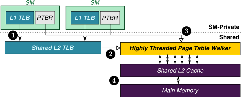
In our GPU-MMU baseline design, a shared L2 TLB entry is extended with address space identifiers. TLB accesses from multiple threads to the same page are coalesced (i.e., combined). On an L1 TLB miss ( in Figure 7.2), the shared L2 TLB is accessed. If the request misses in the shared L2 TLB, the page table walker begins a walk ( ). The walker reads the Page Table Base Register (PTBR)111CR3 in the x86 ISA [173], TTB in the ARM ISA [30]. from the core that caused the TLB miss ( ), which contains a pointer to the root of the page table. The walker then accesses each level of the page table, retrieving the page table data from either the shared L2 cache or the GPU main memory ( ).
Figure 7.3 shows the performance of two GPU-MMU designs: (1) a design that uses the base 4KB page size, and (2) a design that uses a 2MB large page size, where both designs have no demand paging overhead (i.e., the system I/O bus transfer takes zero cycles to transfer a page). We normalize the performance of the two designs to a GPU with an ideal TLB, where all TLB requests hit in the L1 TLB. We make two observations from the figure.

First, compared to the ideal TLB, the GPU-MMU with 4KB base pages experiences an average performance loss of 48.1%. We observe that with 4KB base pages, a single TLB miss often stalls many of the warps, which undermines the latency hiding behavior of the SIMT execution model used by GPUs. Second, the figure shows that using a 2MB page size with the same number of TLB entries as the 4KB design allows applications to come within 2% of the ideal TLB performance. We find that with 2MB pages, the TLB has a much larger reach, which reduces the TLB miss rate substantially. Thus, there is strong incentive to use large pages for address translation.
7.2.2 Large Pages Alone Are Not the Answer
A natural solution to consider is to use only large pages for GPU memory management. Using only large pages would reduce address translation overhead significantly, with minimal changes to the hardware or runtime. Unfortunately, this solution is impractical because large pages (1) greatly increase the data transfer size of each demand paging request, causing contention on the system I/O bus, and harming performance; and (2) waste memory by causing memory bloat due to internal fragmentation.
Demand Paging at a Large Page Granularity. Following the nomenclature from [453], we denote GPU-side page faults that induce demand paging transfers across the system I/O bus as far-faults. Prior work observes that while a 2MB large page size reduces the number of far-faults in GPU applications that exhibit locality, the load-to-use latency (i.e., the time between when a thread issues a load request and when the data is returned to the thread) increases significantly when a far-fault does occur [453]. The impact of far-faults is particularly harmful for workloads with high locality, as all warps touching the 2MB large page frame (i.e., a contiguous, page-aligned 2MB region of physical memory) must stall, which limits the GPU’s ability to overlap the system I/O bus transfer by executing other warps. Based on PCIe latency measurements from a real GTX 1080 system [304], we determine that the load-to-use latency with 2MB large pages () is six times the latency with 4KB base pages ().
Figure 7.4 shows how the GPU performance changes when we use different page sizes and include the effect of the demand paging overhead (see Section 7.4 for our methodology). We make three observations from the figure. First, for 4KB base pages, the demand paging overhead reduces performance, by an average of 40.0% for our single-application workloads, and 82.3% for workloads with five concurrently-executing applications. Second, for our single-application workloads, we find that with demand paging overhead, 2MB pages slow down the execution time by an average of 92.5% compared to 4KB pages with demand paging, as the GPU cores now spend most of their time stalling on the system I/O bus transfers. Third, the overhead of demand paging for larger pages gets significantly worse as more applications share the GPU. With two applications concurrently executing on the GPU, the average performance degradation of demand paging with 2MB pages instead of 4KB pages is 98.0%, and with five applications, the average degradation is 99.8%.
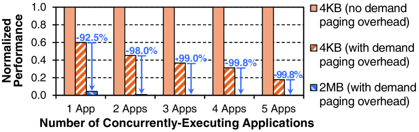
Memory Bloat. Large pages expose the system to internal fragmentation and memory bloat, where a much greater amount of physical memory is allocated than the amount of memory actually needed by an application. To understand the impact of memory bloat, we evaluate the amount of memory allocated to each application when run in isolation, using 4KB and 2MB page sizes. When we use the 4KB base page size, our applications have working sets ranging from 10MB to 362MB, with an average of 81.5MB (see Section 7.4 and [38] for details). We find that the amount of allocated memory inflates by 40.2% on average, and up to 367% in the worst case, when we use 2MB pages instead of 4KB pages (not shown). These numbers are likely conservative, as we expect that the fragmentation would worsen as an application continues to run for longer time scales than we can realistically simulate. Such waste is unacceptable, particularly when there is an increasing demand for GPU memory due to other concurrently-running applications.
We conclude that despite the potential performance gain of 2MB large pages (when the overhead of demand paging is ignored), the demand paging overhead actually causes 2MB large pages to perform much worse than 4KB base pages. As a result, it is impractical to use only 2MB large pages in the GPU. Therefore, a design that delivers the best of both page sizes is needed.
7.2.3 Challenges for Multiple Page Size Support
As Sections 7.2.1 and 7.2.2 demonstrate, we cannot efficiently optimize GPU performance by employing only a single page size. Recent works on TLB design for integrated GPUs [342, 343] and on GPU demand paging support [343, 453, 14, 12, 315] corroborate our own findings on the performance cost of address translation and the performance opportunity of large pages. Our goal is to design a new memory manager for GPUs that efficiently supports multiple page sizes, to exploit the benefits of both small and large page sizes, while avoiding the disadvantages of each. In order to (1) not burden programmers and (2) provide performance improvements for legacy applications, we would like to enable multiple page size support transparently to the application. This constraint introduces several design challenges that must be taken into account.
Page Size Selection. While conceptually simple, multiple page size support introduces complexity for memory management that has traditionally been difficult to handle. Despite architectural support within CPUs [228, 298] for several decades, the adoption of multiple page sizes has been quite slow and application-domain specific [51, 123]. The availability of large pages can either be exposed to application programmers, or managed transparently to an application. Application-exposed management forces programmers to reason about physical memory and use specialized APIs [277, 29] for page management, which usually sacrifices code portability and increases programmer burden. In contrast, application-transparent support (e.g., management by the OS) requires no changes to existing programs to use large pages, but it does require the memory manager to make predictive decisions about whether applications would benefit from large pages. OS-level large page management remains an active research area [228, 298], and the optimization guidance for many modern applications continues to advise strongly against using large pages [280, 86, 337, 356, 302, 407, 392, 428], due to high-latency data transfers over the system I/O bus and memory bloat (as described in Section 7.2.2). In order to provide effective application-transparent support for multiple page sizes in GPUs, we must develop a policy for selecting page sizes that avoids high-latency data transfer over the system I/O bus, and does not introduce significant memory bloat.
Hardware Implementation. Application-transparent support for multiple page sizes requires (1) primitives that implement the transition between different page sizes, and (2) mechanisms that create and preserve contiguity in both the virtual and physical address spaces. We must add support in the GPU to coalesce (i.e., combine) multiple base pages into a single large page, and splinter (i.e., split) a large page back into multiple base pages. While the GPU memory manager can migrate base pages in order to create opportunities for coalescing, base page migration incurs a high latency overhead [374, 71]. In order to avoid the migration overhead without sacrificing coalescing opportunities, the GPU needs to initially allocate data in a coalescing-friendly manner.
GPUs face additional implementation challenges over CPUs, as they rely on hardware-based memory allocation mechanisms and management. In CPU-based application-transparent large page management, coalescing and splintering are performed by the operating system [228, 298], which can (1) use locks and inter-processor interrupts (IPIs) to implement atomic updates to page tables, (2) stall any accesses to the virtual addresses whose mappings are changing, and (3) use background threads to perform coalescing and splintering. GPUs currently have no mechanism to atomically move pages or change page mappings for coalescing or splintering.
7.3 Mosaic
In this section, we describe Mosaic, a GPU memory manager that provides application-transparent support for multiple page sizes and solves the challenges that we discuss in Section 7.2.3. At runtime, Mosaic (1) allocates memory in the GPU such that base pages that are contiguous in virtual memory are contiguous within a large page frame in physical memory (which we call contiguity-conserving allocation; Section 7.3.2); (2) coalesces base pages into a large page frame as soon as the data is allocated, only if all of the pages are i) contiguous in both virtual and physical memory, and ii) belong to the same application (Section 7.3.3); and (3) compacts a large page (i.e., moves the allocated base pages within the large page frame to make them contiguous) if internal fragmentation within the page is high after one of its constituent base pages is deallocated (Section 7.3.4).
7.3.1 High-Level Overview of Mosaic
Figure 7.5 shows the major components of Mosaic, and how they interact with the GPU memory. Mosaic consists of three components: Contiguity-conserving Allocation (CocoA), the Lazy-Coalescer, and Contiguity-aware Compaction (CaC). These three components work together to coalesce (i.e., combine) and splinter (i.e., split apart) base pages to/from large pages during memory management. Memory management operations for Mosaic take place at two times: (1) when memory is allocated, and (2) when memory is deallocated.
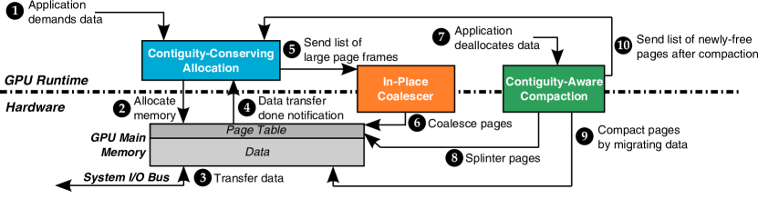
Memory Allocation. When a GPGPU application wants to access data that is not currently in the GPU memory, it sends a request to the GPU runtime (e.g., OpenCL, CUDA runtimes) to transfer the data from the CPU memory to the GPU memory ( in Figure 7.5). A GPGPU application typically allocates a large number of base pages at the same time. CocoAallocates space within the GPU memory ( ) for the base pages, working to conserve the contiguity of base pages, if possible during allocation. Regardless of contiguity, CocoAprovides a soft guarantee that a single large page frame contains base pages from only a single application. Once the base page is allocated, CocoAinitiates the data transfer across the system I/O bus ( ). When the data transfer is complete ( ), CocoAnotifies the Lazy-Coalescer that allocation is done by sending a list of the large page frame addresses that were allocated ( ). For each of these large page frames, the runtime portion of the Lazy-Coalescer then checks to see whether (1) all base pages within the large page frame have been allocated, and (2) the base pages within the large page frame are contiguous in both virtual and physical memory. If both conditions are true, the hardware portion of the Lazy-Coalescer updates the page table to coalesce the base pages into a large page ( ).
Memory Deallocation. When a GPGPU application wants to deallocate memory (e.g., when an application kernel finishes), it sends a deallocation request to the GPU runtime ( ). For all deallocated base pages that are coalesced into a large page, the runtime invokes CaC for the corresponding large page. The runtime portion of CaC checks to see whether the large page has a high degree of internal fragmentation (i.e., if the number of unallocated base pages within the large page exceeds a predetermined threshold). For each large page with high internal fragmentation, the hardware portion of CaC updates the page table to splinter the large page back into its constituent base pages ( ). Next, CaC compacts the splintered large page frames, by migrating data from multiple splintered large page frames into a single large page frame ( ). Finally, CaC notifies CocoAof the large page frames that are now free after compaction ( ), which CocoAcan use for future memory allocations.
7.3.2 Contiguity-Conserving Allocation
Base pages can be coalesced into a large page frame only if (1) all base pages within the frame are contiguous in both virtual and physical memory, (2) the data within the large page frame is page aligned with the corresponding large page within virtual memory (i.e., the first base page within the large page frame is also the first base page of a virtual large page), and (3) all base pages within the frame come from the same virtual address space (e.g., the same application, or the same virtual machine). As Figure 7.1a shows, traditional memory managers allocate base pages without conserving contiguity or ensuring that the base pages within a large page frame belong to the same application. For example, if the memory manager wants to coalesce base pages of Application 1 into a large page frame (e.g., Large Page Frame 1), it must first migrate Application 2’s base pages to another large page frame, and may need to migrate some of Application 1’s base pages within the large page frame to create contiguity. Only after this data migration, the base pages would be ready to be coalesced into a large page frame.
In Mosaic, we minimize the overhead of coalescing pages by designing CocoAto take advantage of the memory allocation behavior of GPGPU applications. Similar to many data-intensive applications [300, 128], GPGPU applications typically allocate memory en masse (i.e., they allocate a large number of pages at a time). The en masse allocation takes place when an application kernel is about to be launched, and the allocation requests are often for a large contiguous region of virtual memory. This region is much larger than the large page size (e.g., 2MB), and Mosaic allocates multiple page-aligned 2MB portions of contiguous virtual memory from the region to large page frames in physical memory, as shown in Figure 7.1b. With CocoA, the large page frames for Application 1 and Application 2 are ready to be coalesced as soon as their base pages are allocated, without the need for any data migration. For all other base pages (e.g., base pages not aligned in the virtual address space, allocation requests that are smaller than a large page), Mosaic simply allocates these pages to any free page, and does not exploit any contiguity.
Mosaic provides a soft guarantee that all base pages within a large page frame belong to the same application, which reduces the cost of performing coalescing and compaction, and ensures that these operations do not violate memory protection. To meet this guarantee during allocation, CocoAneeds to track the application that each large page frame with unallocated base pages is assigned to. The allocator maintains two sets of lists to track this information: (1) the free frame list, a list of free large page frames (i.e., frames where no base pages have been allocated) that are not yet assigned to any application; and (2) free base page lists, per-application lists of free base pages within large page frames where some (but not all) base pages are allocated. When CocoAallocates a page-aligned 2MB region of virtual memory, it takes a large page frame from the free frame list and maps the virtual memory region to the frame. When CocoAallocates base pages in a manner such that it cannot exploit contiguity, it takes a page from the free base page list for the application performing the memory request, to ensure that the soft guarantee is met. If the free base page list for an application is empty, CocoAremoves a large page frame from the free frame list, and adds the frame’s base pages to the free base page list.
Note that there may be cases where the free frame list runs out of large page frames for allocation. We discuss how Mosaic handles such situations in Section 7.3.4.
7.3.3 In-Place Coalescer
In Mosaic, due to CocoA(Section 7.3.2), we find that we can simplify how the page size is selected for each large page frame (i.e., decide which pages should be coalesced), compared to state-of-the-art memory managers. In state-of-the-art memory managers, such as our GPU-MMU baseline based on Power et al. [343], there is no guarantee that base pages within a large page frame belong to the same application, and memory allocators do not conserve virtual memory contiguity in physical memory. As a result, state-of-the-art memory managers must perform four steps to coalesce pages, as shown under the Baseline timeline in Figure 7.6a. First, the manager must identify opportunities for coalescing across multiple pages (not shown in the timeline, as this can be performed in the background). This is done by a hardware memory management unit (MMU), such as the Falcon coprocessor in recent GPU architectures [305], which tallies page utilization information from the page table entries of each base page. The most-utilized contiguous base pages are chosen for coalescing (Pages A–G in Figure 7.6a). Second, the manager must identify a large page frame where the coalesced base pages will reside, and then migrate the base pages to this new large page frame, which uses DRAM channel bandwidth ( in the figure). Third, the manager must update the page table entries (PTEs) to reflect the coalescing, which again uses DRAM channel bandwidth ( ). Fourth, the manager invokes a TLB flush to invalidate stale virtual-to-physical mappings (which point to the base page locations prior to migration), during which the SMs stall ( ). Thus, coalescing using a state-of-the-art memory manager causes significant DRAM channel utilization and SM stalls, as Figure 7.6a shows.

In contrast, Mosaic can perform coalescing in-place, i.e., base pages do not need to be migrated in order to be coalesced into a large page. Hence, we call the page size selection mechanism of Mosaic the Lazy-Coalescer. As shown in Figure 7.6b, the Lazy-Coalescer causes much less DRAM channel utilization and no SM stalls, saving significant waste compared to state-of-the-art memory managers. We describe how the Lazy-Coalescer (1) decides which pages to coalesce, and (2) updates the page table for pages that are coalesced.
Deciding When to Coalesce. Unlike existing memory managers, Mosaic does not need to monitor base page utilization information to identify opportunities for coalescing. Instead, we design CocoAto ensure that the base pages that we coalesce are already allocated to the same large page frame. Once CocoAhas allocated data within a large page frame, it sends the address of the frame to the Lazy-Coalescer. The Lazy-Coalescer then checks to see whether the base pages within the frame are contiguous in both virtual and physical memory.222Coalescing decisions are made purely in the software runtime portion of the Lazy-Coalescer, and thus system designers can easily use a different coalescing policy, if desired. As mentioned in Section 7.3.2, Mosaic coalesces base pages into a large page only if all of the base pages within the large page frame are allocated (i.e., the frame is fully populated). We empirically find that for GPGPU applications, coalescing only contiguous base pages in fully-populated large page frames achieves similar TLB reach to the coalescing performed by existing memory managers (not shown), and avoids the need to employ an MMU or perform page migration, which greatly reduces the overhead of Mosaic.
Coalescing in Hardware. Once the Lazy-Coalescer selects a large page frame for coalescing, it then performs the coalescing operation in hardware. Figure 7.6b shows the steps required for coalescing with the Lazy-Coalescer under the Mosaic timeline. Unlike coalescing in existing memory managers, the Lazy-Coalescer does not need to perform any data migration, as CocoAhas already conserved contiguity within all large page frames selected for coalescing: the coalescing operation needs to only update the page table entries corresponding to the large page frame and the base pages ( in the figure).
We modify the L3 and L4 page table entries (PTEs) to simplify updates during the coalescing operation, as shown in Figure 7.7a. We add a large page bit to each L3 PTE (corresponding to a large page), which is initially set to 0 (to indicate a page that is not coalesced), and we add a disabled bit to each L4 PTE (corresponding to a base page), which is initially set to 0 (to indicate that a page table walker should use the base page virtual-to-physical mapping in the L4 PTE). The coalescing hardware simply needs to locate the L3 PTE for the large page frame being coalesced ( in the figure), and set the large page bit to 1 for the PTE ( ). (We discuss how page table lookups occur below.) We perform this bit setting operation atomically, with a single memory operation to minimize the amount of time before the large page mapping can be used. Then, the coalescing hardware sets the disabled bit to 1 for all L4 PTEs ( ).

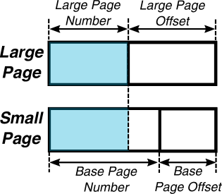
The virtual-to-physical mapping for the large page can be used as soon as the large page bit is set, without (1) waiting for the disabled bits in the L4 PTEs to be set, or (2) requiring a TLB flush to remove the base page mappings from the TLB. This is because no migration was needed to coalesce the base pages into the large page. As a result, the existing virtual-to-physical mappings for the coalesced base pages still point to the correct memory locations. While we set the disabled bits in the PTEs to discourage using these mappings, as the mappings consume a portion of the limited number of base page entries in the TLB, we can continue to use the mappings safely until they are evicted from the TLB. As shown in Figure 7.6b, since we do not flush the TLB, we do not need to stall the SMs. Mosaic ensures that if the coalesced page is subsequently splintered, the large page virtual-to-physical mapping is removed (see Section 7.3.4).333As there is a chance that base pages within a splintered page can migrated during compaction, the large page virtual-to-physical mapping may no longer be valid. To avoid correctness issues when this happens, Mosaic flushes the TLB large page entry for the mapping as soon as a coalesced page is splintered.
As we can see from Figure 7.6, the lack of data migration and TLB flushes in Mosaic greatly reduces the time required for the coalescing operation in Mosaic, with respect to coalescing in existing MMUs.
TLB Lookups After Coalescing. As mentioned in Section 7.1.2, each TLB level contains two separate sets of entries, with one set of entries for each page size. In order to improve TLB reach, we need to ensure that an SM does not fetch the base page PTEs for coalesced base pages (even though these are safe to use) into the TLBs, as these PTEs contend with PTEs of uncoalesced base pages for the limited TLB space. When a GPU with Mosaic needs to translate a memory address, it first checks if the address belongs to a coalesced page by looking up the TLB large page entries. If the SM locates a valid large page entry for the request (i.e., the page is coalesced), it avoids looking up TLB base page entries.
If a TLB miss occurs in both the TLB large page and base page entries for a coalesced page, the page walker traverses the page table. At the L3 PTE ( in Figure 7.7a), the walker reads the large page bit ( ). As the bit is set, the walker needs to read the virtual-to-physical mapping for the large page. The L3 PTE does not typically contain space for a virtual-to-physical mapping, so the walker instead reads the virtual-to-physical mapping from the first PTE of the L4 page table that the L3 PTE points to. Figure 7.7b shows why we can use the mapping in the L4 PTE for the large page. A virtual-to-physical mapping for a large page consists of a page number and an offset. As the base pages within the large page were not migrated, their mappings point to physical memory locations within the large page frame. As a result, if we look at only the bits of the mapping used for the large page number, they are identical for both the large page mapping and the base page mapping. When the large page bit is set, the page walker reads the large page number from the L4 PTE (along with other fields of the PTE, e.g., for access permissions), and returns the PTE to the TLB. In doing so, we do not need to allocate any extra storage for the virtual-to-physical mapping of the large page. Note that for pages that are not coalesced, the page walker behavior is not modified.
7.3.4 Contiguity-Aware Compaction
After an application kernel finishes, it can deallocate some of the base pages that it previously allocated. This deallocation can lead to internal fragmentation within a large page frame that was coalesced, as some of the frame’s constituent base pages are no longer valid. While the page could still benefit from coalescing (as this improves TLB reach), the unallocated base pages within the large page frame cannot be allocated to another virtual address as long as the page remains coalesced. If significant memory fragmentation exists, this can cause CocoAto run out of free large page frames, even though it has not allocated all of the available base pages in GPU memory. To avoid an out-of-memory error in the application, Mosaic uses CaC to splinter and compact highly-fragmented large page frames, freeing up large page frames for CocoAto use.
Deciding When to Splinter and Compact a Coalesced Page. Whenever an application deallocates a base page within a coalesced large page frame, CaC checks to see how many base pages remain allocated within the frame. If the number of allocated base pages falls below a predetermined threshold (which is configurable in the GPU runtime), CaC decides to splinter the large page frame into base pages (see below). Once the splintering operation completes, CaC performs compaction by migrating the remaining base pages to another uncoalesced large page frame that belongs to the same application. In order to avoid occupying multiple memory channels while performing this migration, which can hurt the performance of other threads that are executing concurrently, we restrict CaC to migrate base pages between only large page frames that reside within the same memory channel. After the migration is complete, the original large page frame no longer contains any allocated base pages, and CaC sends the address of the large page frame to CocoA, which adds the address to its free frame list.
If the number of allocated base pages within a coalesced page is greater than or equal to the threshold, CaC does not splinter the page, but notifies CocoAof the large page frame address. CocoAthen stores the coalesced large page frame’s address in a emergency frame list. As a failsafe, if CocoAruns out of free large pages, and CaC does not have any large pages that it can compact, CocoApulls a coalesced page from the emergency frame list, asks CaC to splinter the page, and then uses any unallocated base pages within the splintered large page frame to allocate new virtual base pages.
Splintering the Page in Hardware. Similar to the Lazy-Coalescer, when CaC selects a coalesced page for splintering, it then performs the splintering operation in hardware. The splintering operation essentially reverses the coalescing operation. First, the splintering hardware clears the disabled bit in the L4 PTEs of the constituent base pages. Then, the splintering hardware clears the large page bit atomically, which causes the subsequent page table walks to look up the virtual-to-physical mapping for the base page. Unlike coalescing, when the hardware splinters a coalesced page, it must also issue a TLB flush request for the coalesced page. As we discuss in Section 7.3.3, a large page mapping can be present in the TLB only when a page is coalesced. The flush to the TLB removes the large page entry for this mapping, to ensure synchronization across all SMs with the current state of the page table.
Optimizing Compaction with Bulk Copy Mechanisms. The migration of each base page during compaction requires several long-latency memory operations, where the contents of the page are copied to a destination location only 64 bits at a time, due to the narrow width of the memory channel [374, 242, 378]. To optimize the performance of CaC, we can take advantage of in-DRAM bulk copy techniques such as RowClone [374, 378] or LISA [71], which provide very low-latency (e.g., ) memory copy within a single DRAM module. These mechanisms use existing internal buses within DRAM to copy an entire base page of memory with a single bulk memory operation. While such bulk data copy mechanisms are not essential for our proposal, they have the potential to improve performance when a large amount of compaction takes place. Section 7.5.4 evaluates the benefits of using in-DRAM bulk copy with CaC.
7.4 Methodology
We modify the MAFIA framework [191], which uses GPGPU-Sim 3.2.2 [46], to evaluate Mosaic on a GPU that concurrently executes multiple applications. We have released our simulator modifications [366, 81]. Table 7.1 shows the system configuration we simulate for our evaluations, including the configurations of the GPU core and memory partition (see Section 7.1.1).
| GPU Core Configuration | |
|---|---|
| Shader Core Config | 30 cores, 1020 MHz, GTO warp scheduler [359] |
| Private L1 Cache | 16KB, 4-way associative, LRU, L1 misses are |
| coalesced before accessing L2, 1-cycle latency | |
| Private L1 TLB | 128 base page/16 large page entries per core, |
| fully associative, LRU, single port, 1-cycle latency | |
| Memory Partition Configuration | |
| (6 memory partitions in total, with each partition accessible by all 30 cores) | |
| Shared L2 Cache | 2MB total, 16-way associative, LRU, 2 cache banks and |
| 2 ports per memory partition, 10-cycle latency | |
| Shared L2 TLB | 512 base page/256 large page entries, non-inclusive, |
| 16-way/fully-associative (base page/large page), LRU, | |
| 2 ports, 10-cycle latency | |
| DRAM | 3GB GDDR5, 1674 MHz, 6 channels, 8 banks per rank, |
| FR-FCFS scheduler [357, 454], burst length 8 | |
Simulator Modifications. We modify GPGPU-Sim [46] to model the behavior of Unified Virtual Address Space [310]. We add a memory allocator into cuda-sim, the CUDA simulator within GPGPU-Sim, to handle all virtual-to-physical address translations and to provide memory protection. We add an accurate model of address translation to GPGPU-Sim, including TLBs, page tables, and a page table walker. The page table walker is shared across all SMs, and allows up to 64 concurrent walks. Both the L1 and L2 TLBs have separate entries for base pages and large pages [201, 122, 202, 340, 341, 325]. Each TLB contains miss status holding registers (MSHRs) [226] to track in-flight page table walks. Our simulation infrastructure supports demand paging, by detecting page faults and faithfully modeling the system I/O bus (i.e., PCIe) latency based on measurements from NVIDIA GTX 1080 cards [304] (see Section 7.2.2).444Our experience with the NVIDIA GTX 1080 suggests that production GPUs perform significant prefetching to reduce latencies when reference patterns are predictable. This feature is not modeled in our simulations. We use a worst-case model for the performance of our compaction mechanism (CaC, see Section 7.3.4) conservatively, by stalling the entire GPU (all SMs) and flushing the pipeline. More details about our modifications can be found in our extended technical report [38].
Workloads. We evaluate the performance of Mosaic using both homogeneous and heterogeneous workloads. We categorize each workload based on the number of concurrently-executing applications, which ranges from one to five for our homogeneous workloads, and from two to five for our heterogeneous workloads. We form our homogeneous workloads using multiple copies of the same application. We build 27 homogeneous workloads for each category using GPGPU applications from the Parboil [396], SHOC [90], LULESH [203, 204], Rodinia [77], and CUDA SDK [309] suites. We form our heterogeneous workloads by randomly selecting a number of applications out of these 27 GPGPU applications. We build 25 heterogeneous workloads per category. Each workload has a combined working set size that ranges from 10MB to 2GB. The average working set size of a workload is 217MB. In total we evaluate 235 homogeneous and heterogeneous workloads. We provide a list of all our workloads in our extended technical report [38].
Evaluation Metrics. We report workload performance using the weighted speedup metric [107, 108], which is a commonly-used metric to evaluate the performance of a multi-application workload [33, 209, 221, 220, 293, 292, 287, 94, 93]. Weighted speedup is calculated as:
| (7.1) |
where is the IPC of an application in the workload that runs on the same number of shader cores using the baseline state-of-the-art configuration [343], but does not share GPU resources with any other applications; and is the IPC of the application when it runs concurrently with other applications. We report the performance of each application within a workload using IPC.
Scheduling and Partitioning of Cores. As scheduling is not the focus of this work, we assume that SMs are equally partitioned across the applications within a workload, and use the greedy-then-oldest (GTO) warp scheduler [359]. We speculate that if we use other scheduling or partitioning policies, Mosaic would still increase the TLB reach and achieve the benefits of demand paging effectively, though we leave such studies for future work.
7.5 Evaluation
In this section, we evaluate how Mosaic improves the performance of homogeneous and heterogeneous workloads (see Section 7.4 for more detail). We compare Mosaic to two mechanisms: (1) GPU-MMU, a baseline GPU with a state-of-the-art memory manager based on the work by Power et al. [343], which we explain in detail in Section 7.2.1; and (2) Ideal TLB, a GPU with an ideal TLB, where every address translation request hits in the L1 TLB (i.e., there are no TLB misses).
7.5.1 Homogeneous Workloads
Figure 7.8 shows the performance of Mosaic for the homogeneous workloads. We make two observations from the figure. First, we observe that Mosaic is able to recover most of the performance lost due to the overhead of address translation (i.e., an ideal TLB) in homogeneous workloads. Compared to the GPU-MMU baseline, Mosaic improves the performance by 55.5%, averaged across all 135 of our homogeneous workloads. The performance of Mosaic comes within 6.8% of the Ideal TLB performance, indicating that Mosaic is effective at extending the TLB reach. Second, we observe that Mosaic provides good scalability. As we increase the number of concurrently-executing applications, we observe that the performance of Mosaic remains close to the Ideal TLB performance.
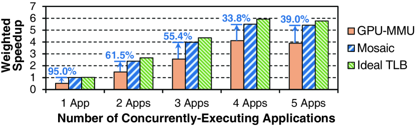
We conclude that for homogeneous workloads, Mosaic effectively approaches the performance of a GPU with the Ideal TLB, by employing multiple page sizes to simultaneously increase the reach of both the L1 private TLB and the shared L2 TLB.
7.5.2 Heterogeneous Workloads
Figure 7.9 shows the performance of Mosaic for heterogeneous workloads that consist of multiple randomly-selected GPGPU applications. From the figure, we observe that on average across all of the workloads, Mosaic provides a performance improvement of 29.7% over GPU-MMU, and comes within 15.4% of the Ideal TLB performance. We find that the improvement comes from the significant reduction in the TLB miss rate with Mosaic, as we discuss below.
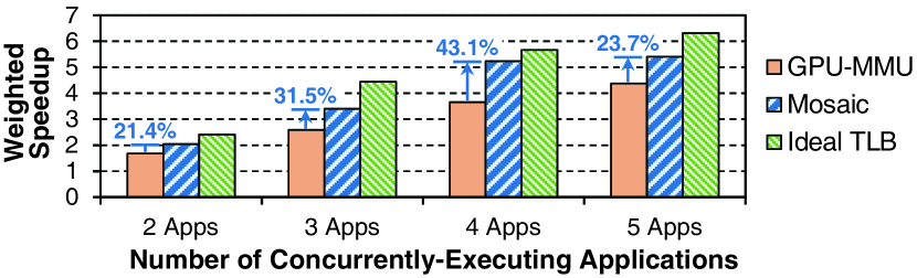
The performance gap between Mosaic and Ideal TLB is greater for heterogeneous workloads than it is for homogeneous workloads. To understand why, we examine the performance of the each workload in greater detail. Figure 7.10 shows the performance improvement of 15 randomly-selected two-application workloads. We categorize the workloads as either TLB-friendly or TLB-sensitive. The majority of the workloads are TLB-friendly, which means that they benefit from utilizing large pages. The TLB hit rate increases significantly with Mosaic (see Section 7.5.3) for TLB-friendly workloads, allowing the workload performance to approach Ideal TLB. However, for TLB-sensitive workloads, such as HS–CONS and NW–HISTO, there is still a performance gap between Mosaic and the Ideal TLB, even though Mosaic improves the TLB hit rate. We discover two main factors that lead to this performance gap. First, in these workloads, one of the applications is highly sensitive to shared L2 TLB misses (e.g., HS in HS–CONS, HISTO in NW–HISTO), while the other application (e.g., CONS, NW) is memory intensive. The memory-intensive application introduces a high number of conflict misses on the shared L2 TLB, which harms the performance of the TLB-sensitive application significantly, and causes the workload’s performance under Mosaic to drop significantly below the Ideal TLB performance. Second, the high latency of page walks due to compulsory TLB misses and higher access latency to the shared L2 TLB (which increases because TLB requests have to probe both the large page and base page TLBs) have a high impact on the TLB-sensitive application. Hence, for these workloads, the Ideal TLB still has significant advantages over Mosaic.

Summary of Impact on Individual Applications. To determine how Mosaic affects the individual applications within the heterogeneous workloads we evaluate, we study the IPC of each application in all of our heterogeneous workloads. In all, this represents a total of 350 individual applications. Figure 7.11 shows the per-application IPC of Mosaic and Ideal TLB normalized to the application’s performance under GPU-MMU, and sorted in ascending order. We show four graphs in the figure, where each graph corresponds to individual applications from workloads with the same number of concurrently-executing applications. We make three observations from these secs/mosaic/results. First, Mosaic improves performance relative to GPU-MMU for 93.6% of the 350 individual applications. We find that the application IPC relative to the baseline GPU-MMU for each application ranges from 66.3% to 860%, with an average of 133.0%. Second, for the 6.4% of the applications where Mosaic performs worse than GPU-MMU, we find that for each application, the other concurrently-executing applications in the same workload experience a significant performance improvement. For example, the worst-performing application, for which Mosaic hurts performance by 33.6% compared to GPU-MMU, is from a workload with three concurrently-executing applications. We find that the other two applications perform 66.3% and 7.8% better under Mosaic, compared to GPU-MMU. Third, we find that, on average across all heterogeneous workloads, 48%, 68.9% and 82.3% of the applications perform within 90%, 80% and 70% of Ideal TLB, respectively.
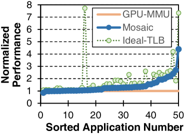
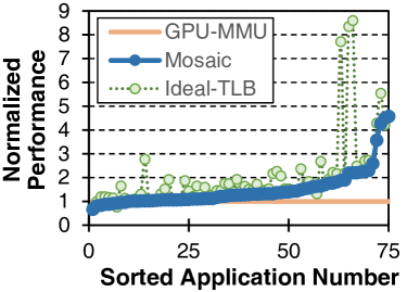
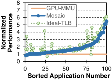
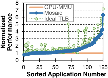
We conclude that Mosaic is effective at increasing the TLB reach for heterogeneous workloads, and delivers significant performance improvements over a state-of-the-art GPU memory manager.
Impact of Demand Paging on Performance. All of our secs/mosaic/results so far show the performance of the GPU-MMU baseline and Mosaic when demand paging is enabled. Figure 7.12 shows the normalized weighted speedup of the GPU-MMU baseline and Mosaic, compared to GPU-MMU without demand paging, where all data required by an application is moved to the GPU memory before the application starts executing. We make two observations from the figure. First, we find that Mosaic outperforms GPU-MMU without demand paging by 58.5% on average for homogeneous workloads and 47.5% on average for heterogeneous workloads. Second, we find that demand paging has little impact on the weighted speedup. This is because demand paging latency occurs only when a kernel launches, at which point the GPU retrieves data from the CPU memory. The data transfer overhead is required regardless of whether demand paging is enabled, and thus the GPU incurs similar overhead with and without demand paging.
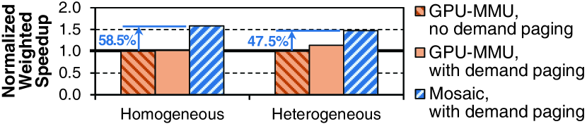
7.5.3 Analysis of TLB Impact
TLB Hit Rate. Figure 7.13 compares the overall TLB hit rate of GPU-MMU to Mosaic for 214 of our 235 workloads, which suffer from limited TLB reach (i.e., workloads that have an L2 TLB hit rate lower than 98%). We make two observations from the figure. First, we observe Mosaic is very effective at increasing the TLB reach of these workloads. We find that for the GPU-MMU baseline, every fully-mapped large page frame contains pages from multiple applications, as the GPU-MMU allocator does not provide the soft guarantee of CocoA. As a result, GPU-MMU does not have any opportunities to coalesce base pages into a large page without performing significant amounts of data migration. In contrast, Mosaic can coalesce a vast majority of base pages thanks to CocoA. As a result, Mosaic reduces the TLB miss rate dramatically for these workloads, with the average miss rate falling below 1% in both the L1 and L2 TLBs. Second, we observe an increasing amount of interference in GPU-MMU when more than three applications are running concurrently. This secs/mosaic/results in a lower TLB hit rate as the number of applications increases from three to four applications, and from four to five applications. The L2 TLB hit rate drops from 81% in workloads with two concurrently-executing applications to 62% in workloads with five concurrently-executing applications. Mosaic experiences no such drop due to interference as we increase the number of concurrently-executing applications, since it makes much greater use of large page coalescing and enables a much larger TLB reach.
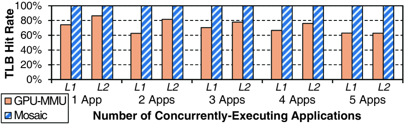
TLB Size Sensitivity. A major benefit of Mosaic is its ability to improve TLB reach by increasing opportunities to coalesce base pages into a large page. After the base pages are coalesced, the GPU uses the large page TLB to cache the virtual-to-physical mapping of the large page, which frees up base page TLB entries so that they can be used to cache mappings for the uncoalesced base pages. We now evaluate how sensitive the performance of Mosaic is to the number of base page and large page entries in each TLB level.
Figure 7.14 shows the performance of both GPU-MMU and Mosaic as we vary the number of base page entries in the per-SM L1 TLBs (Figure 7.14a) and in the shared L2 TLB (Figure 7.14b). We normalize all secs/mosaic/results to the GPU-MMU performance with the baseline 128-base-page-entry L1 TLBs per SM and a 512-base-page-entry shared L2 TLB. From the figure, we make two observations. First, we find that for the L1 TLB, GPU-MMU is sensitive to the number of base page entries, while Mosaic is not sensitive to the number of base page entries. This is because Mosaic successfully coalesces most of its base pages into large pages, which significantly reduces the pressure on TLB base page capacity. In fact, the number of L1 TLB base page entries has a minimal impact on the performance of Mosaic until we scale it all the way down to 8 entries. Even then, compared to an L1 TLB with 128 base page entries, Mosaic loses only 7.6% performance on average with 8 entries. In contrast, we find that GPU-MMU is unable to coalesce base pages, and as a result, its performance scales poorly as we reduce the number of TLB base page entries. Second, we find that the performance of both GPU-MMU and Mosaic is sensitive to the number of L2 TLB base page entries. This is because even though Mosaic does not need many L1 TLB base page entries per SM, the base pages are often shared across multiple SMs. The L2 TLB allows SMs to share page table entries (PTEs) with each other, so that once an SM retrieves a PTE from memory using a page walk, the other SMs do not need to wait on a page walk. The larger the number of L2 TLB base page entries, the more likely it is that a TLB request can avoid the need for a page walk. Since Mosaic does not directly have an effect on the number of page walks, it benefits from a mechanism (e.g., a large L2 TLB) that can reduce the number of page walks and hence is sensitive to the size of the L2 TLB.
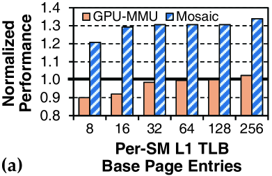

Figure 7.15 shows the performance of both GPU-MMU and Mosaic as we vary the number of large page entries in the per-SM L1 TLBs (Figure 7.15a) and in the shared L2 TLB (Figure 7.15b). We normalize all secs/mosaic/results to the GPU-MMU performance with the baseline 16-large-page-entry L1 TLBs per SM and a 256-large-page-entry shared L2 TLB. We make two observations from the figure. First, for both the L1 and L2 TLBs, Mosaic is sensitive to the number of large page entries. This is because Mosaic successfully coalesces most of its base pages into large pages. We note that the sensitivity is not as high as Mosaic’s sensitivity to L2 TLB base page entries (Figure 7.14b), because each large page entry covers a much larger portion of memory, which allows a smaller number of large page entries to still cover a majority of the total application memory. Second, GPU-MMU is insensitive to the large page entry count. This is because GPU-MMU is unable to coalesce any base pages into large pages, due to its coalescing-unfriendly allocation (see Figure 7.1a). As a result, GPU-MMU makes no use of the large page entries in the TLB.

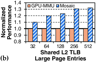
7.5.4 Analysis of the Effect of Fragmentation
When multiple concurrently-executing GPGPU applications share the GPU, a series of memory allocation and deallocation requests could create significant data fragmentation, and could cause CocoAto violate its soft guarantee, as discussed in Section 7.3.2. While we do not observe this behavior in any of the workloads that we evaluate, Mosaic can potentially introduce data fragmentation and memory bloat for very long running applications. In this section, we design stress-test experiments that induce a large amount of fragmentation in large page frames, to study the behavior of CocoAand CaC.
To induce a large amount of fragmentation, we allow the memory allocator to pre-fragment a fraction of the main memory. We randomly place pre-fragmented data throughout the physical memory. This data (1) does not conform to Mosaic’s soft guarantee, and (2) cannot be coalesced with any other base pages within the same large page frame. To vary the degree of large page fragmentation, we define two metrics: (1) the fragmentation index, which is the fraction of large page frames that contain pre-fragmented data; and (2) large page frame occupancy, which is the fraction of the pre-fragmented data that occupies each fragmented large page.
We evaluate the performance of all our workloads on (1) Mosaic with the baseline CaC; and (2) Mosaic with an optimized CaC that takes advantage of in-DRAM bulk copy mechanisms (see Section 7.3.4), which we call CaC-BC. We provide a comparison against two configurations: (1) Ideal CaC, a compaction mechanism where data migration incurs zero latency; and (2) No CaC, where CaC is not applied.
Figure 7.16a shows the performance of CaC when we vary the fragmentation index. For these experiments, we set the large page frame occupancy to 50%. We make three observations from Figure 7.16a. First, we observe that there is minimal performance impact when the fragmentation index is less than 90%, indicating that it is unnecessary to apply CaC unless the main memory is heavily fragmented. Second, as we increase the fragmentation index above 90%, CaC provides performance improvements for Mosaic, as CaC effectively frees up large page frames and prevents CocoAfrom running out of frames. Third, we observe that as the fragmentation index approaches 100%, CaC becomes less effective, due to the fact that compaction needs to be performed very frequently, causing a significant amount of data migration.
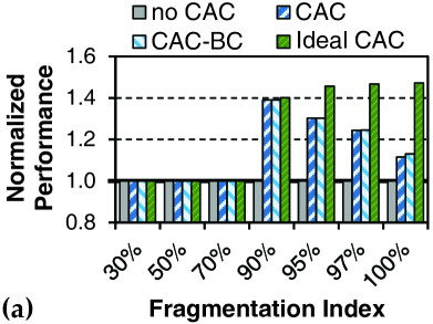
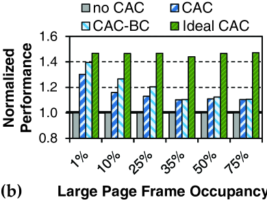
Figure 7.16b shows the performance of CaC as the large page frame occupancy changes when we set the fragmentation index to 100% (i.e., every large page frame is pre-fragmented). We make two observations from the figure. First, we observe that CaC-BC is effective when occupancy is no greater than 25%. When the occupancy is low, in-DRAM bulk-copy operations can effectively reduce the overhead of CaC, as there are many opportunities to free up large page frames that require data migration. Second, we observe that as the occupancy increases beyond 35% (i.e., many base pages are already allocated), the benefits of CaC and CaC-BC decrease, as (1) fewer large page frames can be freed up by compaction, and (2) more base pages need to be moved in order to free a large page frame.
Table 7.2 shows how CaC controls memory bloat for different large page frame occupancies, when we set the fragmentation index to 100%. When large page frames are used, memory bloat can increase as a result of high fragmentation. We observe that when pages are aggressively pre-fragmented, CaC is effective at reducing the memory bloat resulting from high levels of fragmentation. For example, when the large page frame occupancy is very high (e.g., above 75%), CaC compacts the pages effectively, reducing memory bloat to within 2.2% of the memory that would be allocated if we were to use only 4KB pages (i.e., when no large page fragmentation exists). We observe negligible (¡1%) memory bloat when the fragmentation index is less than 100% (not shown), indicating that CaC is effective at mitigating large page fragmentation.
| Large Page Frame | 1% | 10% | 25% | 35% | 50% | 75% |
|---|---|---|---|---|---|---|
| Occupancy (%) | ||||||
| Memory Bloat | 10.66% | 7.56% | 7.20% | 5.22% | 3.37% | 2.22% |
We conclude that CocoAand CaC work together effectively to preserve virtual and physical address contiguity within a large page frame, without incurring high data migration overhead and memory bloat.
7.6 Mosaic: Conclusion
We introduce Mosaic, a new GPU memory manager that provides application-transparent support for multiple page sizes. The key idea of Mosaic is to perform demand paging using smaller page sizes, and then coalesce small (i.e., base) pages into a larger page immediately after allocation, which allows address translation to use large pages and thus increase TLB reach. We have shown that Mosaic significantly outperforms state-of-the-art GPU address translation designs and achieves performance close to an ideal TLB, across a wide variety of workloads. We conclude that Mosaic effectively combines the benefits of large pages and demand paging in GPUs, thereby breaking the conventional tension that exists between these two concepts. We hope the ideas presented in this chapter can lead to future works that analyze Mosaic in detail and provide even lower-overhead support for synergistic address translation and demand paging in heterogeneous systems.
Chapter 8 Common Principles and Lessons Learned
This dissertation introduces several techniques that reduce memory interference in GPU-based systems. In this chapter, we provide a list of common design principles that are used throughout this dissertation as well as a summary of key lessons learned.
8.1 Common Design Principles
While techniques proposed in this dissertation are applied in different parts of the memory hierarchy, they share several key common principles. In this section, we reiterate over these common principles.
Identification of the Benefits of Threads from Using Shared Resources. The first common principle in this dissertation is to give shared resources only to threads that benefit from such shared resources. In many throughput processors, shared resources throughout the memory hierarchy are heavily contended due to the parallelism of these throughput processors. As a result, allowing all threads to freely use these shared resources usually leads to memory interference as we have analyzed thoroughly in Chapters 4, 5, 6 and 7. We observed that intelligently limiting the number of threads that use these shared resources often leads to significant performance improvement of GPU-based systems.
To this end, all mechanisms proposed in this dissertation modify shared resources such that they 1) always prioritize threads that benefit from utilizing shared resources and 2) deprioritize threads that do not benefit from utilizing shared resources to avoid memory interference.
Division of Key Tasks of a Monolithic Structure into Simpler Structures. Another common principle that is utilized is the decoupling of key tasks on monolithic structures throughout the memory hierarchy. In MeDiC and MASK (See Chapters 4 and 6), we provide a mechanism that decouples the monolithic memory request buffer commonly used in modern systems into multiple queues, where different queues deal with different types of GPU memory requests. We found that the division of the monolithic request buffer simplifies the design of the memory scheduler. Specifically, it simplifies memory scheduler logic as the logic can now apply the same scheduling policy on each queue. A similar technique applies to SMS (See Chapter 5), which is a memory controller design for heterogeneous CPU-GPU systems.
8.2 Lessons Learned
This dissertation provides several techniques that together attempt to mitigate the performance impact of memory interference. While our analysis and evaluation have shown that our proposed techniques are effective in reducing the memory interference on various types of GPU-based systems, this dissertation also provides two important lessons. In this section, we summarize these two major lessons learned from our analysis.
Memory Latency is Important for the Performance of Throughput Processors. Typically, limited off-chip memory bandwidth is the major performance bottleneck of throughput processors. In this work, we show that the latency of memory requests also plays an important role in increasing the performance of throughput processors. First, we show that it is possible to reduce the number of cycles many warps are stalled by prioritizing the slowest thread within each warp. Our techniques allow these slow threads to benefit from the lower latency of the shared cache.
Second, we show that the memory latency of the page-walk-related requests is very important to the performance of GPU-based systems. In Chapters 6 and 7, we show that page walks can significantly reduces the memory hiding capability of GPU-based systems. As a result, it is crucial to reduce the latency of these page-walk-related memory requests.
How to Design the GPU Memory Hierarchy to Avoid Memory Interference? This dissertation introduces several techniques across the main memory hierarchy of GPU-based systems. In this section, we provide recommended modifications for the memory hierarchy for both discrete GPUs as well as heterogeneous CPU-GPU systems.
The memory hierarchy of a discrete GPU should be designed to provide high throughput on both single-application and multi-application setups. As a result, the shared L2 data cache, the off-chip main memory and the shared TLB should be designed to minimize memory interference. To this end, MeDiC, MASK, and Mosaic (See Chapters 4, 6 and 7 for the detailed designs and analyses of these mechanisms) can be combined together to improve the efficiency of shared resources (the shared L2 cache, the shared TLB and the main memory). Specifically, we recommend system designers to modify the shared cache to 1) prioritize to threads that benefit from the shared L2 cache (e.g., threads from the mostly-hit and all-hit warp types), 2) deprioritize threads that are less likely to benefit from the shared L2 cache (e.g., threads from the mostly-miss and all-miss warp types), and 3) only cache page-walk-related data that would only benefit from using the shared data cache. Additionally, we recommend system designers to decouple the memory controller to perform two tasks hierarchically. The first task is to divide GPU memory request buffer into three different queues (Golden, Silver and Normal queues) similar to the design of MASK (See Section 6). To combine MASK with MeDiC, requests from the mostly-hit and all-hit warp types should be inserted into the Silver Queue to ensure that these requests have more priority than other data requests. Lastly, system designers should modify the GPU memory allocator to enforce the soft guarantee as defined in Section 7.4, which enables the GPU to provide low-overhead multi-page-size support.
To integrate our techniques into a CPU-GPU heterogeneous system, additional per-application FIFO queues can be integrated into the memory hierarchy as described in Section 5.3. This results in a memory hierarchy design that minimizes all types of memory interference that occur in GPU-based systems.
Chapter 9 Conclusions and Future Directions
In summary, the goal of this dissertation is to develop shared resource management mechanisms that can reduce memory interference in current and future throughput processors. To this end, we analyze memory interference that occurs in Graphics Processing Units, which are the prime example of throughput processors. Based on our analysis of GPU characteristics and the source of memory interference, we categorize memory interference into three different types: intra-application interference, inter-application interference and inter-address-space interference. We propose changes to the cache management and memory scheduling mechanisms to mitigate intra-application interference in GPGPU applications. We propose changes to the memory controller design and its scheduling policy to mitigate inter-application interference in heterogeneous CPU-GPU systems. We redesign the memory management unit and the memory hierarchy in GPUs to be aware of TLB-related data in order to mitigate the inter-address-space interference that originates from the address translation process. We introduce a hardware-software cooperative technique that modifies the memory allocation policy to enable large page support in order to further reduce the inter-address-space interference at the shared TLB. Our evaluations show that the GPU-aware cache and memory management techniques proposed in this dissertation are effective at mitigating the interference caused by GPUs on current and future GPU-based systems.
9.1 Future Research Directions
While this dissertation focuses on methods to mitigate memory interference in various GPU-based systems, this dissertation also uncovers new research topics. In this section, we describe potential research directions to further increase the performance of GPU-based systems.
9.1.1 Improving the Performance of the Memory Hierarchy in GPU-based Systems
Ways to Exploit Emerging High-Bandwidth Memory Technologies. 3D-stacked DRAM [167, 168, 169, 186, 259, 238] is an emerging main memory design that provides high bandwidth and high energy efficiency. We believe that analyzing how this new type of DRAM operates can expose techniques that might benefit modern GPU-based systems.
Aside from 3D-stacked memory, recent proposals provide methods to reduce DRAM latency [239, 70, 240, 241, 222], a method to utilize multi-ported DRAM [242], or methods to perform some computations within DRAM in order to reduce the amount of DRAM bandwidth [373, 374, 71, 163]. We think that these techniques, combined with observations on GPU applications’ characteristics provided in this dissertation, can be applied to GPUs and should provide significant performance improvement for GPU-based systems.
Other Methods to Exploit Warp-type Heterogeneity and TLB-related Data in GPU-based system. In this dissertation, we show in Chapter 4 how GPU-based systems exploit warp-type heterogeneity to reduce intra-application interference and improve the effectiveness of the cache and the main memory. We also show in Chapter 6 how to design a GPU memory hierarchy that is aware of TLB data to minimize inter-address-space interference. We believe that it is beneficial to integrate these warp-type and TLB-awareness characteristics to the memory hierarchy in GPU-based systems to further improve system performance.
Potential Denial-of-service in Software Managed Shared Memory. Allowing GPU-based systems to be shared across multiple GPGPU applications potentially introduces new performance bottlenecks. Concurrently running multiple GPU applications creates a unique resource contention at GPU’s software-managed Shared Scratchpad Memory. Because this particular resource is managed by the GPGPU applications (in software), GPGPU applications that share the GPU all contend for this resource. The lack of communication between each GPGPU application prevents one application to inform its demand for the Shared Scratchpad Memory to other applications. As a result, one application can completely block other applications by using all Shared Scratchpad Memory.
It is possible to solve this unique problem through modifications in the hypervisor. For example, additional kernel scheduling techniques can be applied to 1) probe how much Shared Scratchpad Memory is needed by each application and 2) enforce a proper policy that only grants each application a portion of the Shared Scratchpad Memory.
Interference Management in GPUs for Emerging Applications. The emergence of embedded applications introduces a new requirement: real-time deadlines. Traditionally, these applications run on an embedded device which contains multiple application-specific integrated circuits (ASICs) to handle most of the computations. However, the rise of integrated GPUs in modern System-on-Chips (e.g., [278, 80, 307, 308]) as well as better GPU support in several cloud infrastructures (e.g., [28, 27, 429, 413]) allow these applications to perform these computations on the GPUs. While the GPUs can provide good IPC throughput due to their parallelism, the GPUs and the GPUs’ memory hierarchy, also need to provide a low response time, or in many cases enforce hard performance guarantees (i.e., an application must finish its execution within a certain time limit).
Even though mechanisms proposed in this dissertation aim to minimize the slowdown caused by interference, these mechanisms do not provide actual performance guarantees. However, we believe it is possible to use observations in this dissertation to aid in designing mechanisms to provide a hard performance guarantee and limit the amount of memory interference when multiple of these new embedded applications are concurrently sharing GPU-based systems.
9.1.2 Low-overhead Virtualization Support in GPU-based Systems
While this dissertation proposes mechanisms to minimize inter-address-space interference in GPU-based systems, there are several open-ended research questions on how to efficiently virtualize GPU-based systems and how to efficiently shared other non-memory resources across multiple applications.
Maintaining Virtual Address Space Contiguity. While Chapter 7 provides a mechanism that maintains contiguous physical address, Mosaic does not perform compaction in the virtual address space as this dissertation does not observe virtual address space fragmentation in current GPGPU applications. However, it might be possible that a long chain of small size memory allocations and deallocations can break contiguity within the virtual address space. In this case, the virtual address space has to be remapped in order to create a contiguous chunk of unallocated virtual memory. This can lower the performance of GPU-based systems.
Utilizing High-bandwidth Interconnects to Transfer Data between CPU Memory and GPU Memory. As shown in Chapter 7, demand paging can be costly, especially when a large amount of data has to be transferred to the GPU. The long latency of demand paging can lead to significant stall time for GPU cores. Methods to improve the performance of demand paging remain a potential research problem. Emerging technologies such as NVIDIA’s NVLink [118] and AMD’s Infinity [80] can improve the data transfer rate between the CPUs and the GPUs. However, there is a lack of details on how to integrate these high-bandwidth interconnects to existing GPU hardware. Analyzing how these technologies operate, and providing a detailed study of their potential benefits and limitations is crucial for the integration of these new technologies in GPU-based systems.
Aside from techniques that utilize new technologies, architectural techniques can also mitigate the long data transfer latency between CPU memory and GPU memory. We believe that methods such as preemptively fetching the data of potential pages or proactively evicting potentially unused data in GPU memory can be effective in reducing the performance impact of demand paging.
9.1.3 Providing an Optimal Method to Concurrently Execute GPGPU Applications
While this dissertation allows applications to share the GPUs more efficiently by limiting the memory interference, how to schedule kernels and how to map these kernels to GPU cores remain an open research problem. In this work, we assume 1) an equal partitioning of GPU cores for each GPGPU application, and 2) every application is scheduled to start at the same time. Because applications have a different amount of parallelism as well as bandwidth demand, the optimal number of GPU cores that should be assigned to each application varies not only across different applications, but also across different workload setups.
As a result, providing an optimal method to manage the execution of GPGPU applications on GPU-based systems is a very complex problem. However, we believe that using the knowledge of the resource demand of each application between system software and the GPU hardware can significantly reduce the complexity of the scheduler. Information such as the amount of thread-level parallelism, the expected amount of data parallelism, the expected memory usage, cache locality, memory locality, etc. can be used as hints to assist in providing desirable application-to-GPU-core mappings and kernel scheduling decisions. In this dissertation, we provide several observations regarding GPGPU applications’ characteristics that might be useful for assisting the system software to provide better mapping and scheduling decisions (e.g., memory allocation behavior, warp characteristics).
9.2 Final Summary
We conclude and hope that this dissertation, with the analyses of memory interference and mechanisms to mitigate this memory interference, enables many new research directions that further improve the capability of GPU-based systems.
Other Contributions by the Author
During my Ph.D., I had opportunities to be involved in many other research projects. While these projects do not fit into the theme of this dissertation, they have helped me tremendously in learning an in-depth knowledge about the memory hierarchy as well as the GPU architecture. I would like to acknowledge these projects as well as my early works on Network-on-Chip (NoCs) that kicked start my Ph.D.
My interest in studying memory interference in the memory hierarchy starts from the interests in Network-on-Chip. I have an opportunity in collaborating with Kevin Chang and Chris Fallin on two power-efficient network-on-chip designs that focus on bufferless network-on-chip: HAT [68] and MinBD [110]. In addition, I have authored another work on a hierarchical bufferless network-on-chip design called HiRD [34, 35] and have released NOCulator, which is the simulation infrastructure for both MinBD and HiRD [1]. All these works focus on mechanisms to improve power efficiency and simplifying the design of NoCs without sacrificing system performance. I also have an opportunity collaborating with Reetuparna Das on another work called A2C [91], which studies the placement of applications to cores in NoCs. A2C allows operating systems to be able to place applications to cores in a way that minimize interference, which is also the main theme in this thesis. I worked with Mohammad Fattah on a low-overhead fault-tolerant routing mechanism for network-on-chip [113]. I worked with Besta Maciej on a scalable and energy efficient topology for network-on-chip [52].
In collaboration with Amirali Boroumand, I have worked on using processing-in-memory to improve the energy efficiency of mobile workloads [59].
In collaboration with Vivek Seshadri, I have worked on techniques to allow in-DRAM bulk copy called RowClone [374].
In collaboration with Donghyuk Lee, I have worked on a study that characterizes latency variation in DRAM cells and provides techniques to improve the performance of DRAM by incorporating latency variation [239]
In collaboration with Justin Meza and Hanbin Yoon, I have worked on techniques to manage resources for hybrid memory that consists of DRAM and Phased changed memory (PCM) [442].
In collaboration with Nandita Vijaykumar, I have worked on a technique that allows better utilization of GPU cores called CABA [425]. CABA uses a technique similar to helper threads in order to improve the utilization of GPUs.
In collaboration with Mohammad Sadrosadati, I have worked on a technique to improve the GPU register file performance [365].
In collaboration with Onur Kayiran and Gabriel H. Loh, I have worked on a technique that manages GPU concurrency in a heterogeneous architecture in order to reduce interference [209]. In addition, I also worked on a GPU power management technique that turns down datapath components that are not in the bottleneck [208].
References
- [1] NOCulator. https://github.com/CMU-SAFARI/NOCulator, 2014.
- [2] P. Abad et al. Rotary router: an efficient architecture for CMP interconnection networks. ISCA, 2007.
- [3] M. Abadi, A. Agarwal, P. Barham, E. Brevdo, Z. Chen, C. Citro, G. Corrado, A. Davis, J. Dean, M. Devin, S. Ghemawat, I. Goodfellow, A. Harp, G. Irving, M. Isard, Y. Jia, R. Jozefowicz, L. Kaiser, M. Kudlur, J. Levenberg, D. Mané, R. Monga, S. Moore, D. Murray, C. Olah, M. Schuster, J. Shlens, B. Steiner, I. Sutskever, K. Talwar, P. Tucker, V. Vanhoucke, V. Vasudevan, F. Viégas, O. Vinyals, P. Warden, M. Wattenberg, M. Wicke, Y. Yu, and X. Zheng. TensorFlow: Large-Scale Machine Learning on Heterogeneous Distributed Systems, 2015.
- [4] J. Adriaens, K. Compton, N. S. Kim, and M. Schulte. The Case for GPGPU Spatial Multitasking. In HPCA, 2012.
- [5] Advanced Micro Devices. AMD Accelerated Processing Units.
- [6] Advanced Micro Devices. AMD I/O Virtualization Technology (IOMMU) Specification.
- [7] Advanced Micro Devices. AMD Radeon R9 290X. http://www.amd.com/us/press-releases/Pages/amd-radeon-r9-290x-2013oct24.aspx.
- [8] Advanced Micro Devices. ATI Radeon GPGPUs. http://www.amd.com/us/products/desktop/graphics/amd-radeon-hd-6000/Pages/amd-radeon-hd-6000.aspx.
- [9] Advanced Micro Devices. OpenCL™: The Future of Accelerated Application Performance Is Now.
- [10] Advanced Micro Devices. AMD-V Nested Paging, 2010. http://developer.amd.com/wordpress/media/2012/10/NPT-WP-1%201-final-TM.pdf.
- [11] Advanced Micro Devices. AMD Graphics Cores Next (GCN) Architecture. http://www.amd.com/Documents/GCN_Architecture_whitepaper.pdf, 2012.
- [12] Advanced Micro Devices. Heterogeneous System Architecture: A Technical Review. http://amd-dev.wpengine.netdna-cdn.com/wordpress/media/2012/10/hsa10.pdf, 2012.
- [13] A. Agarwal, B. H. Lim, D. Kranz, and J. Kubiatowicz. APRIL: A Processor Architecture for Multiprocessing. Technical report, Cambridge, MA, USA, 1991.
- [14] N. Agarwal, D. Nellans, M. O’Connor, S. W. Keckler, and T. F. Wenisch. Unlocking Bandwidth for GPUs in CC-NUMA Systems. In HPCA, 2015.
- [15] A. Agrawal, A. Ansari, and J. Torrellas. Mosaic: Exploiting the Spatial Locality of Process Variation to Reduce Refresh Energy in On-chip eDRAM Modules. In HPCA, 2014.
- [16] A. Agrawal, M. O’Connor, E. Bolotin, N. Chatterjee, J. Emer, and S. Keckler. CLARA: Circular Linked-List Auto and Self Refresh Architecture. In MEMSYS, 2016.
- [17] J. Ahn, S. Hong, S. Yoo, O. Mutlu, and K. Choi. A Scalable Processing-in-memory Accelerator for Parallel Graph Processing. In ISCA, 2015.
- [18] J. Ahn, S. Jin, and J. Huh. Revisiting Hardware-Assisted Page Walks for Virtualized Systems. In ISCA, 2012.
- [19] J. Ahn, S. Jin, and J. Huh. Fast Two-Level Address Translation for Virtualized Systems. In IEEE TC, 2015.
- [20] J. Ahn, S. Yoo, O. Mutlu, and K. Choi. PIM-enabled Instructions: A Low-overhead, Locality-aware Processing-in-memory Architecture. In ISCA, 2015.
- [21] J. H. Ahn, N. P. Jouppi, C. Kozyrakis, J. Leverich, and R. S. Schreiber. Improving System Energy Efficiency with Memory Rank Subsetting. ACM TACO, 9(1):4:1–4:28, 2012.
- [22] J. H. Ahn, J. Leverich, R. Schreiber, and N. P. Jouppi. Multicore DIMM: an Energy Efficient Memory Module with Independently Controlled DRAMs. IEEE CAL, 2009.
- [23] B. Akin, F. Franchetti, and J. C. Hoe. Data Reorganization in Memory Using 3D-stacked DRAM. In ISCA, 2015.
- [24] A. R. Alameldeen and D. A. Wood. Interactions Between Compression and Prefetching in Chip Multiprocessors. In HPCA, 2007.
- [25] J. B. Alex Chen and X. Amatriain. Distributed Neural Networks with GPUs in the AWS cloud. 2014.
- [26] R. Alverson, D. Callahan, D. Cummings, B. Koblenz, A. Porterfield, and B. Smith. The Tera Computer System. In ICS, 1990.
- [27] Amazon. Amazon EC2 GPU Instance. http://aws.amazon.com/about-aws/whats-new/2013/11/04/announcing-new-amazon-ec2-gpu-instance-type/.
- [28] Amazon. An Introduction to High Performance Computing on AWS. https://d0.awsstatic.com/whitepapers/Intro_to_HPC_on_AWS.pdf, 2015.
- [29] Apple Inc. Huge Page Support in Mac OS X. [Accessed April-2017].
- [30] ARM Holdings. ARM Cortex-A Series. http://infocenter.arm.com/help/topic/com.arm.doc.den0024a/DEN0024A_v8_architecture_PG.pdf, 2015.
- [31] A. Arunkumar, E. Bolotin, B. Cho, U. Milic, E. Ebrahimi, O. Villa, A. Jaleel, and C.-J. Wu. MCM-GPU: Multi-Chip-Module GPUs for Continued Performance Scalability. In ISCA, 2017.
- [32] R. Ausavarungnirun. Techniques for Shared Resource Management in Systems with Throughput Processors. PhD thesis, Carnegie Mellon Univ., 2017.
- [33] R. Ausavarungnirun, K. Chang, L. Subramanian, G. Loh, and O. Mutlu. Staged Memory Scheduling: Achieving High Performance and Scalability in Heterogeneous Systems. In ISCA, 2012.
- [34] R. Ausavarungnirun, C. Fallin, X. Yu, K. Chang, G. Nazario, R. Das, G. H. Loh, and O. Mutlu. Design and Evaluation of Hierarchical Rings with Deflection Routing. In SBAC-PAD, 2014.
- [35] R. Ausavarungnirun, C. Fallin, X. Yu, K. Chang, G. Nazario, R. Das, G. H. Loh, and O. Mutlu. A Case for Hierarchical Rings with Deflection Routing. PARCO, 54(C):29–45, May 2016.
- [36] R. Ausavarungnirun, S. Ghose, O. Kayıran, G. H. Loh, C. R. Das, M. T. Kandemir, and O. Mutlu. Exploiting Inter-Warp Heterogeneity to Improve GPGPU Performance. In PACT, 2015.
- [37] R. Ausavarungnirun, J. Landgraf, V. Miller, S. Ghose, J. Gandhi, C. J. Rossbach, and O. Mutlu. Mosaic: A GPU Memory Manager with Application-Transparent Support for Multiple Page Sizes. In MICRO, 2017.
- [38] R. Ausavarungnirun, J. Landgraf, V. Miller, S. Ghose, J. Gandhi, C. J. Rossbach, and O. Mutlu. Mosaic: A GPU Memory Manager with Application-Transparent Support for Multiple Page Sizes. Technical Report TR-2017-003, Carnegie Mellon Univ., SAFARI Research Group, 2017.
- [39] R. Ausavarungnirun, V. Miller, J. Landgraf, S. Ghose, J. Gandhi, A. Jog, C. Rossbach, and O. Mutlu. MASK: Redesigning the GPU Memory Hierarchy to Support Multi-Application Concurrency. In ASPLOS, 2018.
- [40] R. Ausavarungnirun, V. Miller, J. Landgraf, S. Ghose, J. Gandhi, A. Jog, C. J. Rossbach, and O. Mutlu. Spatial Multiplexing Support for Multi-Application Concurrency in GPUs. Technical Report TR-2018-002, Carnegie Mellon Univ., SAFARI Research Group, 2018.
- [41] R. Ausavarungnirun, C. J. Rossbach, V. Miller, J. Landgraf, S. Ghose, J. Gandhi, A. Jog, and O. Mutlu. Improving Multi-Application Concurrency Support Within the GPU Memory System. arXiv:1708.04911 [cs.AR], 2017.
- [42] M. Awasthi, D. W. Nellans, K. Sudan, R. Balasubramonian, and A. Davis. Handling the Problems and Opportunities Posed by Multiple On-chip Memory Controllers. In PACT, 2010.
- [43] O. O. Babarinsa and S. Idreos. JAFAR: Near-Data Processing for Databases. In SIGMOD, 2015.
- [44] S. Baek, S. Cho, and R. Melhem. Refresh Now and Then. IEEE TC, 63(12):3114–3126, 2014.
- [45] J.-L. Baer and T.-F. Chen. Effective Hardware-Based Data Prefetching for High-Performance Processors. IEEE TC, 44(5):609–623, 1995.
- [46] A. Bakhoda, G. Yuan, W. Fung, H. Wong, and T. Aamodt. Analyzing CUDA Workloads Using a Detailed GPU Simulator. In ISPASS, 2009.
- [47] P. Baran. On Distributed Communications Networks. 1964.
- [48] G. H. Barnes, R. M. Brown, M. Kato, D. J. Kuck, D. L. Slotnick, and R. A. Stokes. The Illiac IV Computer. IEEE TC, 100(8):746–757, 1968.
- [49] T. W. Barr, A. L. Cox, and S. Rixner. Translation Caching: Skip, Don’T Walk (the Page Table). In ISCA, 2010.
- [50] T. W. Barr, A. L. Cox, and S. Rixner. SpecTLB: A Mechanism for Speculative Address Translation. In ISCA, 2011.
- [51] A. Basu, J. Gandhi, J. Chang, M. D. Hill, and M. M. Swift. Efficient Virtual Memory for Big Memory Servers. In ISCA, 2013.
- [52] M. Besta, S. M. Hassan, S. Yalamanchili, R. Ausavarungnirun, O. Mutlu, and T. Hoefler. Slim NoC: A Low-Diameter On-Chip Network Topology for High Energy Efficiency and Scalability. In ASPLOS, 2018.
- [53] I. Bhati, Z. Chishti, S.-L. Lu, and B. Jacob. Flexible Auto-refresh: Enabling Scalable and Energy-efficient DRAM Refresh Reductions. In ISCA, 2015.
- [54] A. Bhattacharjee. Large-reach Memory Management Unit Caches. In MICRO, 2013.
- [55] A. Bhattacharjee, D. Lustig, and M. Martonosi. Shared Last-level TLBs for Chip Multiprocessors. In HPCA, 2011.
- [56] A. Bhattacharjee and M. Martonosi. Characterizing the TLB Behavior of Emerging Parallel Workloads on Chip Multiprocessors. In PACT, 2009.
- [57] A. Bhattacharjee and M. Martonosi. Inter-core Cooperative TLB for Chip Multiprocessors. In ASPLOS, 2010.
- [58] D. L. Black, R. F. Rashid, D. B. Golub, and C. R. Hill. Translation Lookaside Buffer Consistency: A Software Approach. In ASPLOS, 1989.
- [59] A. Boroumand, S. Ghose, Y. Kim, R. Ausavarungnirun, E. Shiu, R. Thakur, D. Kim, A. Kuusela, A. Knies, P. Ranganathan, and O. Mutlu. Google Workloads for Consumer Devices: Mitigating Data Movement Bottlenecks. In ASPLOS, 2018.
- [60] A. Boroumand, S. Ghose, B. Lucia, K. Hsieh, K. Malladi, H. Zheng, and O. Mutlu. LazyPIM: An Efficient Cache Coherence Mechanism for Processing-in-Memory. IEEE CAL, 2016.
- [61] D. Bouvier and B. Sander. Applying AMD’s ”Kaveri” APU for Heterogeneous Computing. 2014.
- [62] B. Burgess, B. Cohen, J. Dundas, J. Rupley, D. Kaplan, and M. Denman. Bobcat: AMD’s Low-Power x86 Processor. IEEE Micro, 2011.
- [63] M. Burtscher, R. Nasre, and K. Pingali. A Quantitative Study of Irregular Programs on GPUs. In IISWC, 2012.
- [64] P. Cao, E. W. Felten, A. R. Karlin, and K. Li. A Study of Integrated Prefetching and Caching Strategies. In SIGMETRICS, 1995.
- [65] J. Carter, W. Hsieh, L. Stoller, M. Swanson, L. Zhang, E. Brunvand, A. Davis, C.-C. Kuo, R. Kuramkote, M. Parker, L. Schaelicke, and T. Tateyama. Impulse: Building a Smarter Memory Controller. In HPCA, 1999.
- [66] B. Catanzaro, M. Garland, and K. Keutzer. Copperhead: Compiling an Embedded Data Parallel Language. In SIGPLAN, 2011.
- [67] K. Chandrasekar, S. Goossens, C. Weis, M. Koedam, B. Akesson, N. Wehn, and K. Goossens. Exploiting Expendable Process-Margins in DRAMs for Run-Time Performance Optimization. In DATE, 2014.
- [68] K. Chang, R. Ausavarungnirun, C. Fallin, and O. Mutlu. HAT: Heterogeneous Adaptive Throttling for On-Chip Networks. In SBAC-PAD, 2012.
- [69] K. Chang, A. Kashyap, H. Hassan, S. Ghose, K. Hsieh, D. Lee, T. Li, G. Pekhimenko, S. Khan, and O. Mutlu. Understanding Latency Variation in Modern DRAM Chips: Experimental Characterization, Analysis, and Optimization. In SIGMETRICS, 2016.
- [70] K. Chang, D. Lee, Z. Chishti, A. Alameldeen, C. Wilkerson, Y. Kim, and O. Mutlu. Improving DRAM Performance by Parallelizing Refreshes with Accesses . In HPCA, 2014.
- [71] K. Chang, P. J. Nair, D. Lee, S. Ghose, M. K. Qureshi, and O. Mutlu. Low-cost Inter-linked Subarrays (LISA): Enabling Fast Inter-subarray Data Movement in DRAM. In HPCA, 2016.
- [72] K. K. Chang, A. G. Yaglikci, S. Ghose, A. Agrawal, N. Chatterjee, A. Kashyap, D. Lee, M. O’Connor, H. Hassan, and O. Mutlu. Understanding Reduced-Voltage Operation in Modern DRAM Devices: Experimental Characterization, Analysis, and Mechanisms. In SIGMETRIC, 2017.
- [73] N. Chatterjee, M. O’Connor, D. Lee, D. R. Johnson, S. W. Keckler, M. Rhu, and W. J. Dally. Architecting an Energy-Efficient DRAM System for GPUs. In HPCA, 2017.
- [74] N. Chatterjee, M. O’Connor, G. H. Loh, N. Jayasena, and R. Balasubramonian. Managing DRAM Latency Divergence in Irregular GPGPU Applications. In SC, 2014.
- [75] N. Chatterjee, M. Shevgoor, R. Balasubramonian, A. Davis, Z. Fang, R. Illikkal, and R. Iyer. Leveraging Heterogeneity in DRAM Main Memories to Accelerate Critical Word Access. In MICRO, 2012.
- [76] M. Chaudhuri, J. Gaur, N. Bashyam, S. Subramoney, and J. Nuzman. Introducing Hierarchy-awareness in Replacement and Bypass Algorithms for Last-level Caches. In PACT, 2012.
- [77] S. Che, M. Boyer, J. Meng, D. Tarjan, J. Sheaffer, S.-H. Lee, and K. Skadron. Rodinia: A Benchmark Suite for Heterogeneous Computing. In IISWC, 2009.
- [78] X. Chen, L.-W. Chang, C. I. Rodrigues, J. Lv, Z. Wang, and W. W. Hwu. Adaptive Cache Management for Energy-Efficient GPU Computing. In MICRO, 2014.
- [79] X. Chen, S. Wu, L.-W. Chang, W.-S. Huang, C. Pearson, Z. Wang, and W. W. Hwu. Adaptive Cache Bypass and Insertion for Many-Core Accelerators. In MES, 2014.
- [80] M. Clark. A New X86 Core Architecture for the Next Generation of Computing. In HotChips, 2016.
- [81] CMU SAFARI Research Group. https://github.com/CMU-SAFARI.
- [82] J. D. Collins and D. M. Tullsen. Hardware Identification of Cache Conflict Misses. In MICRO, 1999.
- [83] J. Cong, Z. Fang, Y. Hao, and G. Reinmana. Supporting Address Translation for Accelerator-Centric Architectures. In HPCA, 2017.
- [84] Control Data Corporation. Control Data 7600 Computer Systems Reference Manual, 1972.
- [85] R. Cooksey, S. Jourdan, and D. Grunwald. A Stateless, Content-directed Data Prefetching Mechanism. In ASPLOS, 2002.
- [86] Couchbase Inc. Often Overlooked Linux OS Tweaks. [Accessed March, 2014].
- [87] B. A. Crane and J. A. Githens. Bulk Processing in Distributed Logic Memory. IEEE EC, 14(2):186–196, April 1965.
- [88] F. Dahlgren, M. Dubois, and P. Stenström. Sequential Hardware Prefetching in Shared-Memory Multiprocessors. IEEE TPDS, 6(7):733–746, 1995.
- [89] H. Dai, C. Li, H. Zhou, S. Gupta, C. Kartsaklis, and M. Mantor. A Model-driven Approach to Warp/thread-block Level GPU Cache Bypassing. In DAC, 2016.
- [90] A. Danalis, G. Marin, C. McCurdy, J. S. Meredith, P. C. Roth, K. Spafford, V. Tipparaju, and J. S. Vetter. The Scalable Heterogeneous Computing (SHOC) benchmark suite. In GPGPU, 2010.
- [91] R. Das, R. Ausavarungnirun, O. Mutlu, A. Kumar, and M. Azimi. Application-to-core Mapping Policies to Reduce Memory System Interference in Multi-core Systems. In HPCA, 2013.
- [92] R. Das, S. Eachempati, A. K. Mishra, V. Narayanan, and C. R. Das. Design and Evaluation of Hierarchical On-Chip Network Topologies for Next Generation CMPs. HPCA, 2009.
- [93] R. Das, O. Mutlu, T. Moscibroda, and C. R. Das. Application-aware Prioritization Mechanisms for On-chip Networks. In MICRO, 2009.
- [94] R. Das, O. Mutlu, T. Moscibroda, and C. R. Das. Aérgia: Exploiting Packet Latency Slack in On-chip Networks. In ISCA, 2010.
- [95] J. Draper, J. Chame, M. Hall, C. Steele, T. Barrett, J. LaCoss, J. Granacki, J. Shin, C. Chen, C. W. Kang, I. Kim, and G. Daglikoca. The Architecture of the DIVA Processing-in-memory Chip. In ICS, 2002.
- [96] Y. Du, M. Zhou, B. Childers, D. Mosse, and R. Melhem. Supporting Superpages in Non-contiguous Physical Memory. In HPCA, 2015.
- [97] J. Duato, A. Pena, F. Silla, R. Mayo, and E. Quintana-Orti. rCUDA: Reducing the Number of GPU-based Accelerators in High Performance Clusters. In HPCS, 2010.
- [98] T. H. Dunigan. Kendall Square Multiprocessor: Early Experiences and Performance. In of the Intel Paragon, ORNL/TM-12194, 1994.
- [99] N. Duong, D. Zhao, T. Kim, R. Cammarota, M. Valero, and A. V. Veidenbaum. Improving Cache Management Policies Using Dynamic Reuse Distances. In MICRO, 2012.
- [100] E. Ebrahimi, C. J. Lee, O. Mutlu, and Y. N. Patt. Fairness via Source Throttling: A Configurable and High-performance Fairness Substrate for Multi-core Memory Systems. In ASPLOS, 2010.
- [101] E. Ebrahimi, C. J. Lee, O. Mutlu, and Y. N. Patt. Prefetch-aware Shared Resource Management for Multi-core Systems. In ISCA, 2011.
- [102] E. Ebrahimi, C. J. Lee, O. Mutlu, and Y. N. Patt. Fairness via Source Throttling: A Configurable and High-Performance Fairness Substrate for Multi-Core Memory Systems. ACM TOCS, 30(7), 2012.
- [103] E. Ebrahimi, R. Miftakhutdinov, C. Fallin, C. J. Lee, J. A. Joao, O. Mutlu, and Y. N. Patt. Parallel Application Memory Scheduling. In MICRO, 2011.
- [104] E. Ebrahimi, O. Mutlu, C. J. Lee, and Y. N. Patt. Coordinated Control of Multiple Prefetchers in Multi-core Systems. In MICRO, 2009.
- [105] E. Ebrahimi, O. Mutlu, and Y. N. Patt. Techniques for Bandwidth-efficient Prefetching of Linked Data Structures in Hybrid Prefetching Systems. In HPCA, 2009.
- [106] Y. Etsion and D. G. Feitelson. Exploiting Core Working Sets to Filter the L1 Cache with Random Sampling. IEEE TC, 61(11):1535–1550, 2012.
- [107] S. Eyerman and L. Eeckhout. System-Level Performance Metrics for Multiprogram Workloads. IEEE Micro, 28(3), 2008.
- [108] S. Eyerman and L. Eeckhout. Restating the Case for Weighted-IPC Metrics to Evaluate Multiprogram Workload Performance. IEEE CAL, 2014.
- [109] C. Fallin, C. Craik, and O. Mutlu. CHIPPER: A Low-complexity bufferless deflection router. In HPCA, 2011.
- [110] C. Fallin, G. Nazario, X. Yu, K. Chang, R. Ausavarungnirun, and O. Mutlu. MinBD: Minimally-Buffered Deflection Routing for Energy-Efficient Interconnect. In NoCs, 2012.
- [111] C. Fallin, G. Nazario, X. Yu, K. Chang, R. Ausavarungnirun, and O. Mutlu. Bufferless and Minimally-Buffered Deflection Routing, in Routing Algorithms in Networks-on-Chip, pages 241–275. Springer New York, New York, NY, 2014.
- [112] A. Farmahini-Farahani, J. H. Ahn, K. Morrow, and N. S. Kim. NDA: Near-DRAM Acceleration Architecture Leveraging Commodity DRAM Devices and Standard Memory Modules. In HPCA, 2015.
- [113] M. Fattah et al. A Low-Overhead, Fully-Distributed, Guaranteed-Delivery Routing Algorithm for Faulty Network-on-Chips. In NOCS, 2015.
- [114] M. Feng, C. Tian, and R. Gupta. Enhancing LRU Replacement via Phantom Associativity. In INTERACT, Feb 2012.
- [115] J. A. Fisher. Very Long Instruction Word Architectures and the ELI-512. In ISCA, 1983.
- [116] M. Flynn. Very High-Speed Computing Systems. Proc. of the IEEE, 54(2), 1966.
- [117] A. Fog. The Microarchitecture of Intel, AMD and VIA CPUs.
- [118] D. Foley. Ultra-Performance Pascal GPU and NVLink Interconnect. In HotChips.
- [119] B. B. Fraguela, J. Renau, P. Feautrier, D. Padua, and J. Torrellas. Programming the FlexRAM Parallel Intelligent Memory System. In PPoPP, 2003.
- [120] W. Fung, I. Sham, G. Yuan, and T. Aamodt. Dynamic Warp Formation and Scheduling for Efficient GPU Control Flow. In MICRO, 2007.
- [121] W. W. L. Fung and T. M. Aamodt. Thread Block Compaction for Efficient SIMT Control Flow. In HPCA, 2011.
- [122] J. Gandhi, , M. D. Hill, and M. M. Swift. Exceeding the Best of Nested and Shadow Paging. In ISCA, 2016.
- [123] J. Gandhi, A. Basu, M. D. Hill, and M. M. Swift. Efficient Memory Virtualization. In MICRO, 2014.
- [124] H. Gao and C. Wilkerson. A Dueling Segmented LRU Replacement Algorithm with Adaptive Bypassing. In JWAC, 2010.
- [125] M. Gao, G. Ayers, and C. Kozyrakis. Practical Near-Data Processing for In-Memory Analytics Frameworks. In PACT, 2015.
- [126] M. Gao and C. Kozyrakis. HRL: Efficient and Flexible Reconfigurable Logic for Near-data Processing. In HPCA, 2016.
- [127] J. Gaur, M. Chaudhuri, and S. Subramoney. Bypass and Insertion Algorithms for Exclusive Last-Level Caches. In ISCA, 2011.
- [128] D. Gay and A. Aiken. Memory Management with Explicit Regions. In PLDI, 1998.
- [129] M. Gebhart, D. R. Johnson, D. Tarjan, S. W. Keckler, W. J. Dally, E. Lindholm, and K. Skadron. Energy-Efficient Mechanisms for Managing Thread Context in Throughput Processors. In ISCA, 2011.
- [130] S. Ghose, K. Hsieh, A. Boroumand, R. Ausavarungnirun, and O. Mutlu. The Processing-in-Memory Paradigm: Mechanisms to Enable Adoption. In Beyond-CMOS Technologies for Next Generation Computer Design. 2018.
- [131] S. Ghose, H. Lee, and J. F. Martínez. Improving Memory Scheduling via Processor-side Load Criticality Information. In ISCA, 2013.
- [132] M. Gokhale, B. Holmes, and K. Iobst. Processing in Memory: the Terasys Massively Parallel PIM Array. Computer, 28(4):23–31, 1995.
- [133] C. Gómez, M. Gómez, P. López, and J. Duato. Reducing Packet Dropping in a Bufferless NoC. EuroPar, 2008.
- [134] M. Gorman and P. Healy. Supporting Superpage Allocation Without Additional Hardware Support. In ISMM, 2008.
- [135] M. Gorman and P. Healy. Performance Characteristics of Explicit Superpage Support. In WIOSCA, 2010.
- [136] N. Govindaraju, S. Larsen, J. Gray, and D. Manocha. A Memory Model for Scientific Algorithms on Graphics Processors. In SC, 2006.
- [137] J. D. Grimes, L. Kohn, and R. Bharadhwaj. The Intel i860 64-bit Processor: A General-purpose CPU with 3D Graphics Capabilities. IEEE CGA, 9(4):85–94, 1989.
- [138] R. Grindley, T. Abdelrahman, S. Brown, S. Caranci, D. DeVries, B. Gamsa, A. Grbic, M. Gusat, R. Ho, O. Krieger, et al. The NUMAchine Multiprocessor. In ICPP, 2000.
- [139] B. Grot, J. Hestness, S. W. Keckler, and O. Mutlu. Express Cube Topologies for On-Chip Interconnects. In HPCA, 2009.
- [140] B. Grot, J. Hestness, S. W. Keckler, and O. Mutlu. Kilo-NOC: A Heterogeneous Network-on-chip Architecture for Scalability and Service Guarantees. In ISCA, 2011.
- [141] B. Grot, S. Keckler, and O. Mutlu. Topology-aware Quality-of-service Support in Highly Integrated Chip Multiprocessors. In WIOSCA, 2010.
- [142] B. Grot, S. W. Keckler, and O. Mutlu. Preemptive Virtual Clock: A Flexible, Efficient, and Cost-effective QOS Scheme for Networks-on-Chip. In MICRO, 2009.
- [143] M. Gschwind. Chip Multiprocessing and the Cell Broadband Engine. In CF, 2006.
- [144] J. Gummaraju, M. Erez, J. Coburn, M. Rosenblum, and W. J. Dally. Architectural Support for the Stream Execution Model on General-Purpose Processors. In PACT, 2007.
- [145] Q. Guo, N. Alachiotis, B. Akin, F. Sadi, G. Xu, T.-M. Low, L. Pileggi, J. C. Hoe, and F. Franchetti. 3D-Stacked Memory-Side Acceleration: Accelerator and System Design. In WONDP, 2014.
- [146] S. Gupta, H. Gao, and H. Zhou. Adaptive Cache Bypassing for Inclusive Last Level Caches. In IPDPS, 2013.
- [147] D. Gustavson. The Scalable Coherent Interface and Related Standards Projects. IEEE Micro, 1992.
- [148] R. H. Halstead and T. Fujita. MASA: A Multithreaded Processor Architecture for Parallel Symbolic Computing. In ISCA, 1988.
- [149] V. C. Hamacher and H. Jiang. Hierarchical Ring Network Configuration and Performance Modeling. IEEE TC, 2001.
- [150] T. D. Han and T. S. Abdelrahman. Reducing Branch Divergence in GPU Programs. In GPGPU, 2011.
- [151] C. A. Hart. CDRAM in a Unified Memory Architecture. In Intl. Computer Conference, 1994.
- [152] M. Hashemi, Khubaib, E. Ebrahimi, O. Mutlu, and Y. N. Patt. Accelerating Dependent Cache Misses with an Enhanced Memory Controller. In ISCA, 2016.
- [153] M. Hashemi, O. Mutlu, and Y. N. Patt. Continuous Runahead: Transparent Hardware Acceleration for Memory Intensive Workloads. In MICRO, 2016.
- [154] H. Hassan, G. Pekhimenko, N. Vijaykumar, V. Seshadri, D. Lee, O. Ergin, and O. Mutlu. ChargeCache: Reducing DRAM Latency by Exploiting Row Access Locality. In HPCA, 2016.
- [155] H. Hassan, N. Vijaykumar, S. Khan, S. Ghose, K. Chang, G. Pekhimenko, D. Lee, O. Ergin, and O. Mutlu. SoftMC: A Flexible and Practical Open-source Infrastructure for Enabling Experimental DRAM Studies. In HPCA, 2017.
- [156] M. Hayenga, N. E. Jerger, and M. Lipasti. SCARAB: A Single Cycle Adaptive Routing and Bufferless Network. In MICRO, 2009.
- [157] B. He, W. Fang, Q. Luo, N. K. Govindaraju, and T. Wang. Mars: A MapReduce Framework on Graphics Processors. In PACT, 2008.
- [158] H. Hellerman. Parallel Processing of Algebraic Expressions. IEEE Transactions on Electronic Computers, EC-15(1):82–91, Feb 1966.
- [159] A. Herrera. NVIDIA GRID: Graphics Accelerated VDI with the Visual Performance of a Workstation. May 2014.
- [160] H. Hidaka, Y. Matsuda, M. Asakura, and K. Fujishima. The Cache DRAM Architecture. IEEE Micro, 1990.
- [161] W. Hillis. The Connection Machine. MIT Press, 1989.
- [162] S. Hong and H. Kim. An Analytical Model for a GPU Architecture with Memory-Level and Thread-Level Parallelism Awareness. In ISCA, 2009.
- [163] K. Hsieh, E. Ebrahimi, G. Kim, N. Chatterjee, M. O’Connor, N. Vijaykumar, O. Mutlu, and S. W. Keckler. Transparent Offloading and Mapping (TOM): Enabling Programmer-transparent Near-data Processing in GPU Systems. In ISCA, 2016.
- [164] K. Hsieh, S. Khan, N. Vijaykumar, K. K. Chang, A. Boroumand, S. Ghose, and O. Mutlu. Accelerating Pointer Chasing in 3D-stacked Memory: Challenges, Mechanisms, Evaluation. In ICCD, 2016.
- [165] W.-C. Hsu and J. E. Smith. Performance of Cached DRAM Organizations in Vector Supercomputers. In ISCA, 1993.
- [166] I. Hur and C. Lin. Memory Prefetching Using Adaptive Stream Detection. In MICRO, 2006.
- [167] Hybrid Memoty Cube Consortium. High-Bandwidth Memory White Paper.
- [168] Hybrid Memoty Cube Consortium. HMC Specification 1.1, 2013.
- [169] Hybrid Memoty Cube Consortium. HMC Specification 2.0, 2014.
- [170] Hynix. Hynix GDDR5 SGRAM Part H5GQ1H24AFR Revision 1.0.
- [171] T. Ikeda and K. Kise. Application Aware DRAM Bank Partitioning in CMP. In ICPADS, 2013.
- [172] Intel Corp. Intel®I/O Acceleration Technology. http://www.intel.com/content/www/us/en/wireless-network/accel-technology.html.
- [173] Intel Corp. Intel® 64 and IA-32 Architectures Optimization Reference Manual, 2016.
- [174] Intel Corporation. Intel virtualization technology for directed i/o.
- [175] Intel Corporation. Intel(R) Microarchitecture Codename Sandy Bridge. http://www.intel.com/technology/architecture-silicon/2ndgen/.
- [176] Intel Corporation. Sandy Bridge Intel Processor Graphics Performance Developer’s Guide.
- [177] Intel Corporation. Intel architecture mmx™ technology in business applications. 1997. http://download.intel.com/design/PentiumII/papers/24336702.PDF.
- [178] Intel Corporation. Products (Formerly Ivy Bridge), 2012.
- [179] Intel Corporation. Introduction to intel® architecture. 2014. http://www.intel.com/content/dam/www/public/us/en/documents/white-papers/ia-introduction-basics-paper.pdf.
- [180] Intel Corporation. Intel 64 and ia-32 architectures software developer’s manual. 2016. https://www-ssl.intel.com/content/dam/www/public/us/en/documents/manuals/64-ia-32-architectures-software-developer-manual-325462.pdf.
- [181] Intel Corporation. 6th generation intel® core™ processor family datasheet, vol. 1. 2017. http://www.intel.com/content/dam/www/public/us/en/documents/datasheets/desktop-6th-gen-core-family-datasheet-vol-1.pdf.
- [182] B. Jacob and T. Mudge. Virtual Memory in Contemporary Microprocessors. In IEEE Micro, 1998.
- [183] A. Jaleel, W. Hasenplaugh, M. Qureshi, J. Sebot, S. Steely, Jr., and J. Emer. Adaptive Insertion Policies for Managing Shared Caches. In PACT, 2008.
- [184] A. Jaleel, K. B. Theobald, S. C. Steely, Jr., and J. Emer. High Performance Cache Replacement Using Re-reference Interval Prediction (RRIP). In ISCA, 2010.
- [185] J. Jalminger and P. Stenstrom. A Novel Approach to Cache Block Reuse Predictions. In ICPP, 2003.
- [186] JEDEC. High Bandwidth Memory (HBM), 2013.
- [187] M. K. Jeong, M. Erez, C. Sudanthi, and N. Paver. A QoS-Aware Memory Controller for Dynamically Balancing GPU and CPU Bandwidth Use in an MPSoC. In DAC, 2012.
- [188] W. Jia, K. A. Shaw, and M. Martonosi. MRPB: Memory Request Prioritization for Massively Parallel Processors. In HPCA, 2014.
- [189] X. Jiang, Y. Solihin, L. Zhao, and R. Iyer. Architecture Support for Improving Bulk Memory Copying and Initialization Performance. In PACT, 2009.
- [190] A. Jog. Design and Analysis of Scheduling Techniques for Throughput Processors. PhD thesis, Pennsylvania State Univ., 2015.
- [191] A. Jog, O. Kayiran, T. Kesten, A. Pattnaik, E. Bolotin, N. Chatterjee, S. W. Keckler, M. T. Kandemir, and C. R. Das. Anatomy of GPU Memory System for Multi-Application Execution. In MEMSYS, 2015.
- [192] A. Jog, O. Kayıran, A. K. Mishra, M. T. Kandemir, O. Mutlu, R. Iyer, and C. R. Das. Orchestrated Scheduling and Prefetching for GPGPUs. In ISCA, 2013.
- [193] A. Jog, O. Kayıran, N. C. Nachiappan, A. K. Mishra, M. T. Kandemir, O. Mutlu, R. Iyer, and C. R. Das. OWL: Cooperative Thread Array Aware Scheduling Techniques for Improving GPGPU Performance. In ASPLOS, 2013.
- [194] A. Jog, O. Kayiran, A. Pattnaik, M. T. Kandemir, O. Mutlu, R. Iyer, and C. R. Das. Exploiting Core Criticality for Enhanced GPU Performance. In SIGMETRICS, 2016.
- [195] L. K. John and A. Subramanian. Design and Performance Evaluation of A Cache Assist to Implement Selective Caching. In ICCD, 1997.
- [196] D. Joseph and D. Grunwald. Prefetching Using Markov Predictors. In ISCA, 1997.
- [197] N. P. Jouppi. Improving Direct-Mapped Cache Performance by the Addition of a Small Fully-Associative Cache and Prefetch Buffers. In ISCA, 1990.
- [198] J. A. Kahle, M. N. Day, H. P. Hofstee, C. R. Johns, T. R. Maeurer, and D. Shippy. Introduction to the Cell Multiprocessor. IBM JRD, 2005.
- [199] G. B. Kandiraju and A. Sivasubramaniam. Going the Distance for TLB Prefetching: An Application-driven Study. In ISCA, 2002.
- [200] Y. Kang, W. Huang, S.-M. Yoo, D. Keen, Z. Ge, V. Lam, P. Pattnaik, and J. Torrellas. FlexRAM: Toward an Advanced Intelligent Memory System. In ICCD, 1999.
- [201] V. Karakostas, J. Gandhi, F. Ayar, A. Cristal, M. D. Hill, K. S. McKinley, M. Nemirovsky, M. M. Swift, and O. Ünsal. Redundant Memory Mappings for Fast Access to Large Memories. In ISCA, 2015.
- [202] V. Karakostas, J. Gandhi, A. Cristal, M. D. Hill, K. S. McKinley, M. Nemirovsky, M. M. Swift, and O. Unsal. Energy-Efficient Address Translation. In HPCA, 2016.
- [203] I. Karlin, A. Bhatele, J. Keasler, B. Chamberlain, J. Cohen, Z. DeVito, R. Haque, D. Laney, E. Luke, F. Wang, D. Richards, M. Schulz, and C. Still. Exploring Traditional and Emerging Parallel Programming Models using a Proxy Application. In IPDPS, 2013.
- [204] I. Karlin, J. Keasler, and R. Neely. Lulesh 2.0 Updates and Changes. 2013.
- [205] D. Kaseridis, J. Stuecheli, and L. K. John. Minimalist Open-page: A DRAM Page-mode Scheduling Policy for the Many-core Era. In MICRO, 2011.
- [206] S. Kato, M. McThrow, C. Maltzahn, and S. Brandt. Gdev: First-Class GPU Resource Management in the Operating System. In USENIX ATC, 2012.
- [207] O. Kayıran, A. Jog, M. T. Kandemir, and C. R. Das. Neither More Nor Less: Optimizing Thread-Level Parallelism for GPGPUs. In PACT, 2013.
- [208] O. Kayiran, A. Jog, A. Pattnaik, R. Ausavarungnirun, X. Tang, M. T. Kandemir, G. H. Loh, O. Mutlu, and C. R. Das. uC-States: Fine-grained GPU Datapath Power Management. In PACT, 2016.
- [209] O. Kayıran, N. C. Nachiappan, A. Jog, R. Ausavarungnirun, M. T. Kandemir, G. H. Loh, O. Mutlu, and C. R. Das. Managing GPU Concurrency in Heterogeneous Architectures. In MICRO, 2014.
- [210] G. Kedem and R. P. Koganti. WCDRAM: A Fully Associative Integrated Cached-DRAM with Wide Cache Lines. CS-1997-03, Duke, 1997.
- [211] S. Khan et al. PARBOR: An Efficient System-Level Technique to Detect Data Dependent Failures in DRAM. In DSN, 2016.
- [212] S. Khan, D. Lee, Y. Kim, A. R. Alameldeen, C. Wilkerson, and O. Mutlu. The Efficacy of Error Mitigation Techniques for DRAM Retention Failures: A Comparative Experimental Study. In SIGMETRICS, 2014.
- [213] S. Khan, C. Wilkerson, D. Lee, A. R. Alameldeen, and O. Mutlu. A Case for Memory Content-Based Detection and Mitigation of Data-Dependent Failures in DRAM. In IEEE CAL, 2016.
- [214] S. Khan, C. Wilkerson, Z. Wang, A. R. Alameldeen, D. Lee, and O. Mutlu. Detecting and Mitigating Data-dependent DRAM Failures by Exploiting Current Memory Content. In MICRO, 2017.
- [215] M. Kharbutli and Y. Solihin. Counter-Based Cache Replacement and Bypassing Algorithms. IEEE TC, 57(4):433–447, Apr. 2008.
- [216] Khronos OpenCL Working Group. The OpenCL Specification. http://www.khronos.org/registry/cl/specs/opencl-1.0.29.pdf, 2008.
- [217] J. Kim and M. C. Papaefthymiou. Block-based Multi-period Refresh for Energy Efficient Dynamic Memory. In ASIC, 2001.
- [218] J. S. Kim, D. Senol, H. Xin, D. Lee, S. Ghose, M. Alser, H. Hassan, O. Ergin, C. Alkan, and O. Mutlu. GRIM-Filter: Fast Seed Location Filtering in DNA Read Mapping Using Processing-in-Memory Technologies. BMC Genomics, 2018.
- [219] K. Kim and J. Lee. A New Investigation of Data Retention Time in Truly Nanoscaled DRAMs. In EDL, 2009.
- [220] Y. Kim, D. Han, O. Mutlu, and M. Harchol-Balter. ATLAS: A Scalable and High-Performance Scheduling Algorithm for Multiple Memory Controllers. In HPCA, 2010.
- [221] Y. Kim, M. Papamichael, O. Mutlu, and M. Harchol-Balter. Thread Cluster Memory Scheduling: Exploiting Differences in Memory Access Behavior. In MICRO, 2010.
- [222] Y. Kim, V. Seshadri, D. Lee, J. Liu, and O. Mutlu. A Case for Exploiting Subarray-Level Parallelism (SALP) in DRAM. In ISCA, 2012.
- [223] A. K. Kodi, A. Sarathy, and A. Louri. iDEAL: Inter-router Dual-function Energy and Area-efficient Links for Network-on-chip (NoC) Architectures. In ISCA, 2008.
- [224] P. M. Kogge. EXECUBE-A New Architecture for Scaleable MPPs. In ICPP, 1994.
- [225] S. Konstantinidou and L. Snyder. Chaos Router: Architecture and Performance. In ISCA, 1991.
- [226] D. Kroft. Lockup-Free Instruction Fetch/Prefetch Cache Organization. In ISCA, 1981.
- [227] E. Kultursay, M. Kandemir, A. Sivasubramaniam, and O. Mutlu. Evaluating STT-RAM as an energy-efficient main memory alternative. In ISPASS, 2013.
- [228] Y. Kwon, H. Yu, S. Peter, C. J. Rossbach, and E. Witchel. Coordinated and Efficient Huge Page Management with Ingens. In OSDI, 2016.
- [229] A.-C. Lai, C. Fide, and B. Falsafi. Dead-block Prediction & Dead-block Correlating Prefetchers. In ISCA, 2001.
- [230] B. Langmead and S. L. Salzberg. Fast Gapped-Read Alignment with Bowtie 2. Nature Methods, 2012.
- [231] B. C. Lee, E. Ipek, O. Mutlu, and D. Burger. Architecting Phase Change Memory as a Scalable DRAM Alternative. In ISCA, 2009.
- [232] B. C. Lee, E. Ipek, O. Mutlu, and D. Burger. Phase Change Memory Architecture and the Quest for Scalability. CACM, 53(7):99–106, 2010.
- [233] B. C. Lee, P. Zhou, J. Yang, Y. Zhang, B. Zhao, E. Ipek, O. Mutlu, and D. Burger. Phase-Change Technology and the Future of Main Memory. IEEE Micro, 30(1):143–143, 2010.
- [234] C. J. Lee, O. Mutlu, V. Narasiman, and Y. N. Patt. Prefetch-aware DRAM Controllers. In MICRO, 2008.
- [235] C. J. Lee, O. Mutlu, V. Narasiman, and Y. N. Patt. Prefetch-aware Memory Controllers. IEEE TC, 60(10):1406–1430, 2011.
- [236] C. J. Lee, V. Narasiman, E. Ebrahimi, O. Mutlu, and Y. N. Patt. DRAM-aware Last-level Cache Writeback: Reducing Write-caused Interference in Memory Systems. In TR-HPS-2010-002, April, 2010.
- [237] C. J. Lee, V. Narasiman, O. Mutlu, and Y. N. Patt. Improving Memory Bank-Level Parallelism in the Presence of Prefetching. In MICRO, 2009.
- [238] D. Lee, S. Ghose, G. Pekhimenko, S. Khan, and O. Mutlu. Simultaneous Multi-layer Access: Improving 3D-stacked Memory Bandwidth at Low Cost. ACM TACO, 12(4):63, 2016.
- [239] D. Lee, S. Khan, L. Subramanian, S. Ghose, R. Ausavarungnirun, G. Pekhimenko, V. Seshadri, and O. Mutlu. Design-Induced Latency Variation in Modern DRAM Chips: Characterization, Analysis, and Latency Reduction Mechanisms. In SIGMETRICS, 2017.
- [240] D. Lee, Y. Kim, G. Pekhimenko, S. Khan, V. Seshadri, K. Chang, and O. Mutlu. Adaptive-latency DRAM: Optimizing DRAM Timing for the Common-case. In HPCA, 2015.
- [241] D. Lee, Y. Kim, V. Seshadri, J. Liu, L. Subramanian, and O. Mutlu. Tiered-latency DRAM: A Low Latency and Low Cost DRAM Architecture. In HPCA, 2013.
- [242] D. Lee, L. Subramanian, R. Ausavarungnirun, J. Choi, and O. Mutlu. Decoupled Direct Memory Access: Isolating CPU and IO Traffic by Leveraging a Dual-Data-Port DRAM. In PACT, 2015.
- [243] S.-Y. Lee and C.-J. Wu. Characterizing GPU Latency Hiding Ability. In ISPASS, 2014.
- [244] J. Leng, T. Hetherington, A. ElTantawy, S. Gilani, N. S. Kim, T. M. Aamodt, and V. J. Reddi. GPUWattch: Enabling Energy Optimizations in GPGPUs. In ISCA, 2013.
- [245] A. Li, G.-J. van den Braak, A. Kumar, and H. Corporaal. Adaptive and Transparent Cache Bypassing for GPUs. In SC, 2015.
- [246] C. Li, S. L. Song, H. Dai, A. Sidelnik, S. K. S. Hari, and H. Zhou. Locality-Driven Dynamic GPU Cache Bypassing. In ICS, 2015.
- [247] D. Li, M. Rhu, D. Johnson, M. O’Connor, M. Erez, D. Burger, D. Fussell, and S. Redder. Priority-Based Cache Allocation in Throughput Processors. In HPCA, 2015.
- [248] T. Li, V. K. Narayana, and T. El-Ghazawi. Symbiotic Scheduling of Concurrent GPU Kernels for Performance and Energy Optimizations. In CF, 2014.
- [249] Huge Pages Part 2 (Interfaces). https://lwn.net/Articles/375096/. [February, 2010].
- [250] C. H. Lin, D. Y. Shen, Y. J. Chen, C. L. Yang, and M. Wang. SECRET: Selective Error Correction for Refresh Energy Reduction in DRAMs. In ICCD, 2012.
- [251] E. Lindholm, J. Nickolls, S. Oberman, and J. Montrym. NVIDIA Tesla: A Unified Graphics and Computing Architecture. IEEE Micro, 28(2), 2008.
- [252] H. Liu, M. Ferdman, J. Huh, and D. Burger. Cache Bursts: A New Approach for Eliminating Dead Blocks and Increasing Cache Efficiency. In MICRO, 2008.
- [253] J. Liu, B. Jaiyen, Y. Kim, C. Wilkerson, and O. Mutlu. An Experimental Study of Data Retention Behavior in Modern DRAM Devices: Implications for Retention Time Profiling Mechanisms. In ISCA, 2013.
- [254] J. Liu, B. Jaiyen, R. Veras, and O. Mutlu. RAIDR: Retention-aware Intelligent DRAM Refresh. In ISCA, 2012.
- [255] L. Liu, Z. Cui, M. Xing, Y. Bao, M. Chen, and C. Wu. A Software Memory Partition Approach for Eliminating Bank-level Interference in Multicore Systems. In PACT, 2012.
- [256] W. Liu, P. Huang, T. Kun, T. Lu, K. Zhou, C. Li, and X. He. LAMS: A Latency-aware Memory Scheduling Policy for Modern DRAM Systems. In IPCCC, 2016.
- [257] W. Liu, W. Muller-Wittig, and B. Schmidt. Performance Predictions for General-Purpose Computation on GPUs. In ICPP, 2007.
- [258] W. Liu, B. Schmidt, G. Voss, and W. Muller-Wittig. Accelerating Molecular Dynamics Simulations using Graphics Processing Units with CUDA. Computer Physics Communications, 179(9):634–641, 2008.
- [259] G. H. Loh. 3D-stacked Memory Architectures for Multi-core Processors. In ISCA, 2008.
- [260] S.-L. Lu, Y.-C. Lin, and C.-L. Yang. Improving DRAM Latency with Dynamic Asymmetric Subarray. In MICRO, 2015.
- [261] C.-K. Luk, R. Cohn, R. Muth, H. Patil, A. Klauser, G. Lowney, S. Wallace, V. J. Reddi, and K. Hazelwood. Pin: Building Customized Program Analysis Tools with Dynamic Instrumentation. In PLDI, 2005.
- [262] Y. Luo, S. Govindan, B. Sharma, M. Santaniello, J. Meza, A. Kansal, J. Liu, B. Khessib, K. Vaid, and O. Mutlu. Characterizing Application Memory Error Vulnerability to Optimize Datacenter Cost via Heterogeneous-Reliability Memory. In DSN, 2014.
- [263] D. Lustig, A. Bhattacharjee, and M. Martonosi. TLB Improvements for Chip Multiprocessors: Inter-Core Cooperative Prefetchers and Shared Last-Level TLBs. ACM TACO, 2013.
- [264] L. Ma and R. Chamberlain. A Performance Model for Memory Bandwidth Constrained Applications on Graphics Engines. In ASAP, 2012.
- [265] K. Mai, T. Paaske, N. Jayasena, R. Ho, W. J. Dally, and M. Horowitz. Smart Memories: A Modular Reconfigurable Architecture. In ISCA, 2000.
- [266] M. Mao, W. Wen, X. Liu, J. Hu, D. Wang, Y. Chen, and H. Li. TEMP: Thread Batch Enabled Memory Partitioning for GPU. In DAC, 2016.
- [267] T. Mashimo, Y. Fukunishi, N. Kamiya, Y. Takano, I. Fukuda, and H. Nakamura. Molecular Dynamics Simulations Accelerated by GPU for Biological Macromolecules with a Non-Ewald Scheme for Electrostatic Interactions. Journal of Chemical Theory and Computation, 2013.
- [268] C. McNairy and D. Soltis. Itanium 2 Processor Microarchitecture. IEEE Micro, 23(2):44–55, 2003.
- [269] X. Mei and X. Chu. Dissecting GPU Memory Hierarchy Through Microbenchmarking. IEEE TPDS, 28(1):72–86, Jan 2017.
- [270] V. Mekkat, A. Holey, P.-C. Yew, and A. Zhai. Managing Shared Last-Level Cache in a Heterogeneous Multicore Processor. In PACT, 2013.
- [271] J. Meng, D. Tarjan, and K. Skadron. Dynamic Warp Subdivision for Integrated Branch and Memory Divergence Tolerance. In ISCA, 2010.
- [272] J. Menon, M. de Kruijf, and K. Sankaralingam. iGPU: Exception Support and Speculative Execution on GPUs. In ISCA, 2012.
- [273] J. Meza, J. Chang, H. Yoon, O. Mutlu, and P. Ranganathan. Enabling Efficient and Scalable Hybrid Memories Using Fine-Granularity DRAM Cache Management. IEEE CAL, 2012.
- [274] J. Meza, J. Li, and O. Mutlu. A Case for Small Row Buffers in Non-Volatile Main Memories. In ICCD, 2012.
- [275] J. Meza, Y. Luo, S. Khan, J. Zhao, Y. Xie, and O. Mutlu. A Case for Efficient Hardware/Software Cooperative Management of Storage and Memory. In WEED, 2013.
- [276] Micron Technology, Inc. 576Mb: x18, x36 RLDRAM3, 2011.
- [277] Microsoft Corporation. Large-Page Support in Windows. [Accessed April-2017].
- [278] R. Mijat. Take GPU Processing Power Beyond Graphics with Mali GPU Computing, 2012.
- [279] A. K. Mishra, O. Mutlu, and C. R. Das. A Heterogeneous Multiple Network-on-chip Design: An Application-aware Approach. In DAC, 2013.
- [280] MongoDB Inc. Disable Transparent Huge Pages (THP). [Accessed April, 2016].
- [281] T. Moscibroda and O. Mutlu. Memory Performance Attacks: Denial of Memory Service in Multi-core Systems. In USENIX Security, 2007.
- [282] T. Moscibroda and O. Mutlu. Distributed Order Scheduling and Its Application to Multi-core DRAM Controllers. In PODC, 2008.
- [283] T. Moscibroda and O. Mutlu. A Case for Bufferless Routing in On-Chip Networks. In ISCA, 2009.
- [284] D. Mrozek, M. Brozek, and B. Malysiak-Mrozek. Parallel Implementation of 3D Protein Structure Similarity Searches Using a GPU and the CUDA. Journal of Molecular Modeling, 2014.
- [285] J. Mukundan and J. F. Martinez. MORSE: Multi-objective Reconfigurable Self-optimizing Memory Scheduler. In HPCA, 2012.
- [286] R. Mullins, A. West, and S. Moore. Low-latency Virtual-channel Routers for On-chip Networks. In ISCA, 2004.
- [287] S. P. Muralidhara, L. Subramanian, O. Mutlu, M. Kandemir, and T. Moscibroda. Reducing Memory Interference in Multicore Systems via Application-Aware Memory Channel Partitioning. In MICRO, 2011.
- [288] N. Muralimanohar, R. Balasubramonian, and N. Jouppi. Optimizing NUCA Organizations and Wiring Alternatives for Large Caches with CACTI 6.0. In MICRO, 2007.
- [289] O. Mutlu. Memory Scaling: A Systems Architecture Perspective. In IMW, 2013.
- [290] O. Mutlu, H. Kim, and Y. N. Patt. Address-value Delta (AVD) Prediction: Increasing the Effectiveness of Runahead Execution by Exploiting Regular Memory Allocation Patterns. In MICRO, 2005.
- [291] O. Mutlu, H. Kim, and Y. N. Patt. Techniques for Efficient Processing in Runahead Execution Engines. In ISCA, 2005.
- [292] O. Mutlu and T. Moscibroda. Stall-Time Fair Memory Access Scheduling for Chip Multiprocessors. In MICRO, 2007.
- [293] O. Mutlu and T. Moscibroda. Parallelism-Aware Batch Scheduling: Enhancing Both Performance and Fairness of Shared DRAM Systems. In ISCA, 2008.
- [294] O. Mutlu, J. Stark, C. Wilkerson, and Y. N. Patt. Runahead Execution: An Alternative to Very Large Instruction Windows for Out-of-Order Processors. In HPCA, 2003.
- [295] O. Mutlu and L. Subramanian. Research Problems and Opportunities in Memory Systems. SUPERFRI, 2015.
- [296] P. J. Nair, D.-H. Kim, and M. K. Qureshi. ArchShield: Architectural Framework for Assisting DRAM Scaling by Tolerating High Error Rates. In ISCA, 2013.
- [297] V. Narasiman, M. Shebanow, C. J. Lee, R. Miftakhutdinov, O. Mutlu, and Y. N. Patt. Improving GPU Performance via Large Warps and Two-Level Warp Scheduling. In MICRO, 2011.
- [298] J. Navarro, S. Iyer, P. Druschel, and A. Cox. Practical, Transparent Operating System Support for Superpages. In OSDI, 2002.
- [299] K. J. Nesbit, A. S. Dhodapkar, and J. E. Smith. AC/DC: An Adaptive Data Cache Prefetcher. In PACT, 2004.
- [300] K. Nguyen, L. Fang, G. Xu, B. Demsky, S. Lu, S. Alamian, and O. Mutlu. Yak: A High-Performance Big-Data-Friendly Garbage Collector. In OSDI, 2016.
- [301] M. S. Nobile, P. Cazzaniga, A. Tangherloni, and D. Besozzi. Graphics Processing Units in Bioinformatics, Computational Biology and Systems Biology. Briefings in Bioinformatics, 2016.
- [302] NuoDB Inc. Linux Transparent Huge Pages, JEMalloc and NuoDB. [Accessed May, 2014].
- [303] NVIDIA Corp. Tesla K40 GPU Active Accelerator. https://www.nvidia.com/content/PDF/kepler/Tesla-K40-Active-Board-Spec-BD-06949-001_v03.pdf, 2013.
- [304] NVIDIA Corp. NVIDIA GeForce GTX 1080. https://international.download.nvidia.com/geforce-com/international/pdfs/GeForce_GTX_1080_Whitepaper_FINAL.pdf, 2016.
- [305] NVIDIA Corp. NVIDIA RISC-V Story. https://riscv.org/wp-content/uploads/2016/07/Tue1100_Nvidia_RISCV_Story_V2.pdf, 2016.
- [306] NVIDIA Corp. CUDA Toolkit Documentation. http://docs.nvidia.com/cuda/cuda-runtime-api/stream-sync-behavior.html, 2017.
- [307] NVIDIA Corporation. NVIDIA Tegra K1.
- [308] NVIDIA Corporation. NVIDIA® Tegra® X1.
- [309] NVIDIA Corporation. CUDA C/C++ SDK Code Samples. http://developer.nvidia.com/cuda-cc-sdk-code-samples, 2011.
- [310] NVIDIA Corporation. NVIDIA’s Next Generation CUDA Compute Architecture: Fermi. http://www.nvidia.com/content/pdf/fermi_white_papers/nvidia_fermi_compute_architecture_whitepaper.pdf, 2011.
- [311] NVIDIA Corporation. NVIDIA’s Next Generation CUDA Compute Architecture: Kepler GK110. http://www.nvidia.com/content/PDF/kepler/NVIDIA-Kepler-GK110-Architecture-Whitepaper.pdf, 2012.
- [312] NVIDIA Corporation. NVIDIA GeForce GTX 750 Ti. 2014.
- [313] NVIDIA Corporation. CUDA C Programming Guide. http://docs.nvidia.com/cuda/cuda-c-programming-guide/index.html, 2015.
- [314] NVIDIA Corporation. Multi-Process Service. https://docs.nvidia.com/deploy/pdf/CUDA_Multi_Process_Service_Overview.pdf, 2015.
- [315] NVIDIA Corporation. NVIDIA Tesla P100. https://images.nvidia.com/content/pdf/tesla/whitepaper/pascal-architecture-whitepaper.pdf, 2016.
- [316] NVIDIA Corporation. Parallel Thread Execution ISA Version 5.0. 2017.
- [317] NVIDIA Corporation. Tuning CUDA Applications for Maxwell. 2017.
- [318] G. Nychis, C. Fallin, T. Moscibroda, and O. Mutlu. Next Generation On-Chip Networks: What Kind of Congestion Control Do We Need? In Hotnets, 2010.
- [319] G. Nychis, C. Fallin, T. Moscibroda, O. Mutlu, and S. Seshan. On-chip Networks from a Networking Perspective: Congestion and Scalability in Many-core Interconnects. In SIGCOMM, 2012.
- [320] S. O, Y. H. Son, N. S. Kim, and J. H. Ahn. Row-Buffer Decoupling: A Case for Low-Latency DRAM Microarchitecture. In ISCA, 2014.
- [321] T. Ohsawa, K. Kai, and K. Murakami. Optimizing the DRAM Refresh Count for Merged DRAM/Logic LSIs. In ISLPED, 1998.
- [322] M. Oskin, F. T. Chong, and T. Sherwood. Active Pages: A Computation Model for Intelligent Memory. In ISCA, 1998.
- [323] S. Pai, M. J. Thazhuthaveetil, and R. Govindarajan. Improving GPGPU Concurrency with Elastic Kernels. In ASPLOS, 2013.
- [324] S. Palacharla, N. P. Jouppi, and J. E. Smith. Complexity-effective Superscalar Processors. In ISCA, 1997.
- [325] M.-M. Papadopoulou, X. Tong, A. Seznec, and A. Moshovos. Prediction-based Superpage-friendly TLB Designs. In HPCA, 2015.
- [326] J. Park, R. M. Yoo, D. S. Khudia, C. J. Hughes, and D. Kim. Location-aware Cache Management for Many-core Processors with Deep Cache Hierarchy. In SC, 2013.
- [327] M. Patel, J. Kim, and O. Mutlu. The Reach Profiler (REAPER): Enabling the Mitigation of DRAM Retention Failures via Profiling at Aggressive Conditions. In ISCA, 2017.
- [328] H. Patil, R. Cohn, M. Charney, R. Kapoor, A. Sun, and A. Karunanidhi. Pinpointing Representative Portions of Large Intel Itanium Programs with Dynamic Instrumentation. In MICRO, 2004.
- [329] D. Patterson, T. Anderson, N. Cardwell, R. Fromm, K. Keeton, C. Kozyrakis, R. Thomas, and K. Yelick. A Case for Intelligent RAM. IEEE Micro, 17(2):34–44, 1997.
- [330] A. Pattnaik, X. Tang, A. Jog, O. Kayiran, A. K. Mishra, M. T. Kandemir, O. Mutlu, and C. R. Das. Scheduling Techniques for GPU Architectures with Processing-In-Memory Capabilities. In PACT, 2016.
- [331] PCI-SIG. PCI Express Base Specification Revision 3.1a, 2015.
- [332] G. Pekhimenko, E. Bolotin, N. Vijaykumar, O. Mutlu, T. C. Mowry, and S. W. Keckler. A Case for Toggle-aware Compression for GPU Systems. In HPCA, 2016.
- [333] G. Pekhimenko, T. Huberty, R. Cai, O. Mutlu, P. B. Gibbons, M. A. Kozuch, and T. C. Mowry. Exploiting Compressed Block Size as an Indicator of Future Reuse. In HPCA, 2015.
- [334] G. Pekhimenko, V. Seshadri, Y. Kim, H. Xin, O. Mutlu, M. A. Kozuch, P. B. Gibbons, and T. C. Mowry. Linearly Compressed Pages: A Main Memory Compression Framework with Low Complexity and Low Latency. In MICRO, 2013.
- [335] G. Pekhimenko, V. Seshadri, O. Mutlu, P. B. Gibbons, M. A. Kozuch, and T. C. Mowry. Base-delta-immediate Compression: Practical Data Compression for On-chip Caches. In PACT, 2012.
- [336] A. Peleg and U. Weiser. MMX Technology Extension to the Intel Architecture. IEEE Micro, 16(4):51–59, August 1996.
- [337] Percona. Why TokuDB Hates Transparent HugePages. [Accessed July, 2014].
- [338] S. Phadke and S. Narayanasamy. MLP Aware Heterogeneous Memory System. In DATE, 2011.
- [339] B. Pham, A. Bhattacharjee, Y. Eckert, and G. H. Loh. Increasing TLB Reach by Exploiting Clustering in Page Translations. In HPCA, 2014.
- [340] B. Pham, V. Vaidyanathan, A. Jaleel, and A. Bhattacharjee. CoLT: Coalesced Large-Reach TLBs. In MICRO, 2012.
- [341] B. Pham, J. Vesely, G. Loh, and A. Bhattacharjee. Large Pages and Lightweight Memory Management in Virtualized Systems: Can You Have it Both Ways? In MICRO, 2015.
- [342] B. Pichai, L. Hsu, and A. Bhattacharjee. Architectural Support for Address Translation on GPUs: Designing Memory Management Units for CPU/GPUs with Unified Address Spaces. In ASPLOS, 2014.
- [343] J. Power, M. D. Hill, and D. A. Wood. Supporting x86-64 Address Translation for 100s of GPU Lanes. In HPCA, 2014.
- [344] PowerVR. PowerVR Hardware Architecture Overview for Developers. 2016. http://cdn.imgtec.com/sdk-documentation/PowerVR+Hardware.Architecture+Overview+for+Developers.pdf.
- [345] T. Preis, P. Virnau, W. Paul, and J. J. Schneider. Accelerated Fluctuation Analysis by Graphic Cards and Complex Pattern Formation in Financial Markets. New Journal of Physics, 11, 2009.
- [346] S. H. Pugsley, J. Jestes, H. Zhang, R. Balasubramonian, V. Srinivasan, A. Buyuktosunoglu, A. Davis, and F. Li. NDC: Analyzing the Impact of 3D-stacked Memory+logic Devices on MapReduce Workloads. In ISPASS, 2014.
- [347] M. K. Qureshi, A. Jaleel, Y. N. Patt, S. C. Steely, and J. Emer. Adaptive Insertion Policies for High Performance Caching. In ISCA, 2007.
- [348] M. K. Qureshi, J. Karidis, M. Franceschini, V. Srinivasan, L. Lastras, and B. Abali. Enhancing Lifetime and Security of PCM-based Main Memory with Start-gap Wear Leveling. In MICRO, 2009.
- [349] M. K. Qureshi, D. H. Kim, S. Khan, P. J. Nair, and O. Mutlu. AVATAR: A Variable-Retention-Time (VRT) Aware Refresh for DRAM Systems. In DSN, 2015.
- [350] M. K. Qureshi and Y. N. Patt. Utility-based Cache Partitioning: A Low-overhead, High-performance, Runtime Mechanism to Partition Shared Caches. In MICRO, 2006.
- [351] M. K. Qureshi, V. Srinivasan, and J. A. Rivers. Scalable High Performance Main Memory System Using Phase-change Memory Technology. In ISCA, 2009.
- [352] B. R. Rau. Pseudo-randomly Interleaved Memory. In ISCA, 1991.
- [353] G. Ravindran and M. Stumm. A Performance Comparison of Hierarchical Ring- and Mesh-connected Multiprocessor Networks. In HPCA, 1997.
- [354] G. Ravindran and M. Stumm. On Topology and Bisection Bandwidth for Hierarchical-ring Networks for Shared Memory Multiprocessors. In HPCA, 1998.
- [355] V. J. Reddi, A. Settle, D. A. Connors, and R. S. Cohn. PIN: A Binary Instrumentation Tool for Computer Architecture Research and Education. In WCAE, 2004.
- [356] Redis Labs. Redis Latency Problems Troubleshooting. [Accessed April, 2016].
- [357] S. Rixner, W. J. Dally, U. J. Kapasi, P. Mattson, and J. D. Owens. Memory Access Scheduling. In ISCA, 2000.
- [358] T. G. Rogers. Locality and Scheduling in the Massively Multithreaded Era. PhD thesis, Univ. of British Columbia, 2015.
- [359] T. G. Rogers, M. O’Connor, and T. M. Aamodt. Cache-Conscious Wavefront Scheduling. In MICRO, 2012.
- [360] T. G. Rogers, M. O’Connor, and T. M. Aamodt. Divergence-Aware Warp Scheduling. In MICRO, 2013.
- [361] B. F. Romanescu, A. R. Lebeck, D. J. Sorin, and A. Bracy. UNified Instruction/Translation/Data (UNITD) Coherence: One Protocol to Rule them All. In HPCA, 2010.
- [362] C. J. Rossbach, J. Currey, M. Silberstein, B. Ray, and E. Witchel. PTask: Operating System Abstractions to Manage GPUs as Compute Devices. In SOSP, 2011.
- [363] C. J. Rossbach, Y. Yu, J. Currey, J.-P. Martin, and D. Fetterly. Dandelion: A Compiler and Runtime for Heterogeneous Systems. In SIGOPS, 2013.
- [364] R. M. Russell. The CRAY-1 Computer System. CACM, 21(1):63–72, 1978.
- [365] M. Sadrosadati, A. Mirhosseini, B. Ehsani, H. Sarbazi-Azad, M. P. Drumond, B. Falsafi, R. Ausavarungnirun, and O. Mutlu. LTRF: A Latency Tolerant Register File Architecture for GPUs. In ASPLOS, 2018.
- [366] SAFARI Research Group. Mosaic – GitHub Repository. https://github.com/CMU-SAFARI/Mosaic/.
- [367] Y. Sato, T. Suzuki, T. Aikawa, S. Fujioka, W. Fujieda, H. Kobayashi, H. Ikeda, T. Nagasawa, A. Funyu, Y. Fuji, K. Kawasaki, M. Yamazaki, and M. Taguchi. Fast cycle RAM (FCRAM): A 20-ns Random Row Access, Pipe-Lined Operating DRAM. In VLSIC, 1998.
- [368] A. Saulsbury, F. Dahlgren, and P. Stenström. Recency-based TLB Preloading. In ISCA, 2000.
- [369] P. B. Schneck. The CDC STAR-100, pages 99–117. Springer US, Boston, MA, 1987.
- [370] D. N. Senzig and R. V. Smith. Computer Organization for Array Processing. In AFIPS, 1965.
- [371] S.-Y. Seo. Methods of Copying a Page in a Memory Device and Methods of Managing Pages in a Memory System. U.S. Patent Application 20140185395, 2014.
- [372] V. Seshadri, A. Bhowmick, O. Mutlu, P. B. Gibbons, M. A. Kozuch, and T. C. Mowry. The Dirty-Block Index. In ISCA, 2014.
- [373] V. Seshadri, K. Hsieh, A. Boroumand, D. Lee, M. Kozuch, O. Mutlu, P. Gibbons, and T. Mowry. Fast Bulk Bitwise AND and OR in DRAM. IEEE CAL, 2015.
- [374] V. Seshadri, Y. Kim, C. Fallin, D. Lee, R. Ausavarungnirun, G. Pekhimenko, Y. Luo, O. Mutlu, P. B. Gibbons, M. A. Kozuch, et al. RowClone: Fast and Energy-efficient in-DRAM Bulk Data Copy and Initialization. In ISCA, 2013.
- [375] V. Seshadri, D. Lee, T. Mullins, H. Hassan, A. Boroumand, J. Kim, M. A. Kozuch, O. Mutlu, P. B. Gibbons, and T. C. Mowry. Buddy-RAM: Improving the Performance and Efficiency of Bulk Bitwise Operations Using DRAM. In arXiv CoRR, 2016.
- [376] V. Seshadri, D. Lee, T. Mullins, H. Hassan, A. Boroumand, J. Kim, M. A. Kozuch, O. Mutlu, P. B. Gibbons, and T. C. Mowry. Ambit: In-Memory Accelerator for Bulk Bitwise Operations Using Commodity DRAM Technology. In MICRO, 2017.
- [377] V. Seshadri, T. Mullins, A. Boroumand, O. Mutlu, P. B. Gibbons, M. A. Kozuch, and T. C. Mowry. Gather-Scatter DRAM: In-DRAM Address Translation to Improve the Spatial Locality of Non-Unit Strided Accesses. In MICRO, 2015.
- [378] V. Seshadri and O. Mutlu. Simple Operations in Memory to Reduce Data Movement. In Advances in Computers. 2017.
- [379] V. Seshadri, O. Mutlu, M. A. Kozuch, and T. C. Mowry. The Evicted-Address Filter: A Unified Mechanism to Address Both Cache Pollution and Thrashing. In PACT, 2012.
- [380] V. Seshadri, S. Yedkar, H. Xin, O. Mutlu, P. B. Gibbons, M. A. Kozuch, and T. C. Mowry. Mitigating Prefetcher-Caused Pollution Using Informed Caching Policies for Prefetched Blocks. ACM TACO, 11(4):51:1–51:22, 2015.
- [381] T. Shanley. Pentium Pro Processor System Architecture. Addison-Wesley Longman Publishing Co., Inc., Boston, MA, USA, 1st edition, 1996.
- [382] W. Shin, J. Yang, J. Choi, and L.-S. Kim. NUAT: A Non-Uniform Access Time Memory Controller. In HPCA, 2014.
- [383] J. Sim, A. Dasgupta, H. Kim, and R. Vuduc. A Performance Analysis Framework for Identifying Potential Benefits in GPGPU Applications. In PPoPP, 2012.
- [384] J. Sim, G. H. Loh, H. Kim, M. O’Connor, and M. Thottethodi. A Mostly-Clean DRAM Cache for Effective Hit Speculation and Self-Balancing Dispatch. In MICRO, 2012.
- [385] I. Singh, A. Shriraman, W. W. L. Fung, M. O’Connor, and T. M. Aamodt. Cache Coherence for GPU Architectures. In HPCA, 2013.
- [386] SiSoftware. Benchmarks : Measuring GP (GPU/APU) Cache and Memory Latencies. http://www.sisoftware.net, 2014.
- [387] R. L. Sites and R. T. Witek. ALPHA Architecture Reference Manual. Digital Press, Boston, Oxford, Melbourne, 1998.
- [388] D. L. Slotnick, W. C. Borck, and R. C. McReynolds. The Solomon Computer – A Preliminary Report. In Workshop on Computer Organization, 1962.
- [389] B. Smith. Architecture and Applications of the HEP Multiprocessor Computer System. SPIE, 1981.
- [390] B. J. Smith. A Pipelined, Shared Resource MIMD Computer. In ICPP, 1978.
- [391] Y. H. Son, S. O, Y. Ro, J. W. Lee, and J. H. Ahn. Reducing Memory Access Latency with Asymmetric DRAM Bank Organizations. In ISCA, 2013.
- [392] Splunk Inc. Transparent Huge Memory Pages and Splunk Performance. [Accessed December, 2013].
- [393] S. Srikantaiah and M. Kandemir. Synergistic TLBs for High Performance Address Translation in Chip Multiprocessors. In MICRO, 2010.
- [394] S. Srinath, O. Mutlu, H. Kim, and Y. N. Patt. Feedback Directed Prefetching: Improving the Performance and Bandwidth-Efficiency of Hardware Prefetchers. In HPCA, 2007.
- [395] H. S. Stone. A Logic-in-Memory Computer. IEEE TC, C-19(1):73–78, 1970.
- [396] J. A. Stratton, C. Rodrigrues, I.-J. Sung, N. Obeid, L. Chang, G. Liu, and W.-M. W. Hwu. Parboil: A Revised Benchmark Suite for Scientific and Commercial Throughput Computing. Technical Report IMPACT-12-01, University of Illinois at Urbana-Champaign, Urbana, Mar. 2012.
- [397] J. Stuecheli, D. Kaseridis, D. Daly, H. C. Hunter, and L. K. John. The Virtual Write Queue: Coordinating DRAM and Last-level Cache Policies. In ISCA, 2010.
- [398] L. Subramanian, D. Lee, V. Seshadri, H. Rastogi, and O. Mutlu. The Blacklisting Memory Scheduler: Achieving high performance and fairness at low cost. In ICCD, 2014.
- [399] L. Subramanian, D. Lee, V. Seshadri, H. Rastogi, and O. Mutlu. The Blacklisting Memory Scheduler: Balancing Performance, Fairness and Complexity. arXiv CoRR, 2015.
- [400] L. Subramanian, D. Lee, V. Seshadri, H. Rastogi, and O. Mutlu. BLISS: Balancing Performance, Fairness and Complexity in Memory Access Scheduling. In IEEE TPDS, 2016.
- [401] L. Subramanian, V. Seshadri, A. Ghosh, S. Khan, and O. Mutlu. The Application Slowdown Model: Quantifying and Controlling the Impact of Inter-application Interference at Shared Caches and Main Memory. In MICRO, 2015.
- [402] L. Subramanian, V. Seshadri, Y. Kim, B. Jaiyen, and O. Mutlu. MISE: Providing Performance Predictability and Improving Fairness in Shared Main Memory Systems. In HPCA, 2013.
- [403] A. K. Sujeeth, K. J. Brown, H. Lee, T. Rompf, H. Chafi, M. Odersky, and K. Olukotun. Delite: A Compiler Architecture for Performance-oriented Embedded Domain-specific Languages. In TECS, 2014.
- [404] Z. Sura, A. Jacob, T. Chen, B. Rosenburg, O. Sallenave, C. Bertolli, S. Antao, J. Brunheroto, Y. Park, K. O’Brien, and R. Nair. Data Access Optimization in a Processing-in-memory System. In CF, 2015.
- [405] R. S. Sutton and A. G. Barto. Reinforcement Learning: An Introduction, volume 1.
- [406] Y. Suzuki, S. Kato, H. Yamada, and K. Kono. GPUvm: Why Not Virtualizing GPUs at the Hypervisor? In USENIX ATC, 2014.
- [407] Sybase Inc. SAP IQ and Linux Hugepages/Transparent Hugepages. [Accessed May, 2014].
- [408] M. Talluri and M. D. Hill. Surpassing the TLB Performance of Superpages with Less Operating System Support. In ASPLOS, 1994.
- [409] I. Tanasic, I. Gelado, J. Cabezas, A. Ramirez, N. Navarro, and M. Valero. Enabling Preemptive Multiprogramming on GPUs. In ISCA, 2014.
- [410] J. E. Thornton. Parallel Operation in the Control Data 6600. AFIPS FJCC, 1964.
- [411] J. E. Thornton. Design of a Computer—the Control Data 6600. 1970.
- [412] Transparent Hugepages. https://lwn.net/Articles/359158/. [October, 2009].
- [413] K. Tian, Y. Dong, and D. Cowperthwaite. A Full GPU Virtualization Solution with Mediated Pass-Through. In USENIX ATC, 2014.
- [414] G. Tyson, M. Farrens, J. Matthews, and A. R. Pleszkun. A Modified Approach to Data Cache Management. In MICRO, 1995.
- [415] Univ. of British Columbia. GPGPU-Sim GTX 480 Configuration. http://dev.ece.ubc.ca/projects/gpgpu-sim/browser/v3.x/configs/GTX480.
- [416] H. Usui, L. Subramanian, K. Chang, and O. Mutlu. SQUASH: Simple qos-aware high-performance memory scheduler for heterogeneous systems with hardware accelerators. arXiv CoRR, 2015.
- [417] H. Usui, L. Subramanian, K. Chang, and O. Mutlu. DASH: Deadline-Aware High-Performance Memory Scheduler for Heterogeneous Systems with Hardware Accelerators. ACM TACO, 12(4), Jan. 2016.
- [418] H. Vandierendonck and A. Seznec. Fairness Metrics for Multi-threaded Processors. IEEE CAL, Feb 2011.
- [419] R. Venkatesan, S. Herr, and E. Rotenberg. Retention-aware Placement in DRAM (RAPID): Software Methods for Quasi-non-volatile DRAM. In HPCA, 2006.
- [420] J. Vesely, A. Basu, M. Oskin, G. H. Loh, and A. Bhattacharjee. Observations and Opportunities in Architecting Shared Virtual Memory for Heterogeneous Systems. In ISPASS, 2016.
- [421] T. Vijayaraghavany, Y. Eckert, G. H. Loh, M. J. Schulte, M. Ignatowski, B. M. Beckmann, W. C. Brantley, J. L. Greathouse, W. Huang, A. Karunanithi, O. Kayiran, M. Meswani, I. Paul, M. Poremba, S. Raasch, S. K. Reinhardt, G. Sadowski, and V. Sridharan. Design and Analysis of an APU for Exascale Computing. In HPCA, 2017.
- [422] N. Vijaykumar, E. Ebrahimi, K. Hsieh, P. B. Gibbons, and O. Mutlu. The Locality Descriptor: A Holistic Abstraction to Exploit Data Locality in GPUs. In ISCA, 2018.
- [423] N. Vijaykumar, K. Hsieh, G. Pekhimenko, S. Khan, A. Shrestha, S. Ghose, A. Jog, P. B. Gibbons, and O. Mutlu. Zorua: A Holistic Approach to Resource Virtualization in GPUs. In MICRO, 2016.
- [424] N. Vijaykumar, A. Jain, D. Majumdar, K. Hsieh, G. Pekhimenko, E. Ebrahimi, N. Hajinazar, P. B. Gibbons, and O. Mutlu. A Case for Richer Cross-layer Abstractions: Bridging the Semantic Gap to Enhance Memory Optimization. In ISCA, 2018.
- [425] N. Vijaykumar, G. Pekhimenko, A. Jog, A. Bhowmick, R. Ausavarungnirun, C. Das, M. Kandemir, T. C. Mowry, and O. Mutlu. A Case for Core-Assisted Bottleneck Acceleration in GPUs: Enabling Flexible Data Compression with Assist Warps. In ISCA, 2015.
- [426] N. Vijaykumar, G. Pekhimenko, A. Jog, A. Bhowmick, R. Ausavarungnirun, C. Das, M. Kandemir, T. C. Mowry, and O. Mutlu. A Framework for Accelerating Bottlenecks in GPU Execution with Assist Warps. In Advances in GPU Research and Practice. 2016.
- [427] Vivante. Vivante Vega GPGPU Technology. 2016. http://www.vivantecorp.com/index.php/en/technology/gpgpu.html.
- [428] VoltDB Inc. VoltDB Documentation. [Accessed April, 2016].
- [429] L. Vu, H. Sivaraman, and R. Bidarkar. GPU Virtualization for High Performance General Purpose Computing on the ESX Hypervisor. In HPC, 2014.
- [430] Z. Wang, J. Yang, R. Melhem, B. R. Childers, Y. Zhang, and M. Guo. Simultaneous Multikernel GPU: Multi-tasking Throughput Processors via Fine-Grained Sharing. In HPCA, 2016.
- [431] F. A. Ware and C. Hampel. Improving Power and Data Efficiency with Threaded Memory Modules. In ICCD, 2006.
- [432] S. Wasson. AMD’s A8-3800 Fusion APU., Oct. 2011.
- [433] H. Wong, M.-M. Papadopoulou, M. Sadooghi-Alvandi, and A. Moshovos. Demystifying GPU Microarchitecture Through Microbenchmarking. In ISPASS, 2010.
- [434] Y. Wu, R. Rakvic, L.-L. Chen, C.-C. Miao, G. Chrysos, and J. Fang. Compiler Managed Micro-cache Bypassing for High Performance EPIC Processors. In MICRO, 2002.
- [435] L. Xiang, T. Chen, Q. Shi, and W. Hu. Less Reused Filter: Improving L2 Cache Performance via Filtering Less Reused Lines. In ICS, 2009.
- [436] P. Xiang, Y. Yang, and H. Zhou. Warp-Level Divergence in GPUs: Characterization, Impact, and Mitigation. In HPCA, 2014.
- [437] M. Xie, D. Tong, K. Huang, and X. Cheng. Improving System Throughput and Fairness Simultaneously in Shared Memory CMP Systems via Dynamic Bank Partitioning. In HPCA, 2014.
- [438] X. Xie, Y. Liang, G. Sun, and D. Chen. An Efficient Compiler Framework for Cache Bypassing on GPUs. In ICCAD, 2013.
- [439] X. Xie, Y. Liang, Y. Wang, G. Sun, and T. Wang. Coordinated Static and Dynamic Cache Bypassing for GPUs. In HPCA, 2015.
- [440] D. Xiong, K. Huang, X. Jiang, and X. Yan. Memory Access Scheduling Based on Dynamic Multilevel Priority in Shared DRAM Systems. ACM TACO, 13(4), Dec. 2016.
- [441] Q. Xu, H. Jeon, K. Kim, W. W. Ro, and M. Annavaram. Warped-Slicer: Efficient Intra-SM Slicing through Dynamic Resource Partitioning for GPU Multiprogramming. In ISCA, 2016.
- [442] H. Yoon, J. Meza, R. Ausavarungnirun, R. Harding, and O. Mutlu. Row Buffer Locality Aware Caching Policies for Hybrid Memories. In ICCD, 2012.
- [443] B. Yu, J. Ma, T. Chen, and M. Wu. Global Priority Table for Last-Level Caches. In DASC, 2011.
- [444] X. Yu, C. J. Hughes, N. Satish, O. Mutlu, and S. Devadas. Banshee: Bandwidth-Efficient DRAM Caching via Software/Hardware Cooperation. In MICRO, 2017.
- [445] G. Yuan, A. Bakhoda, and T. Aamodt. Complexity Effective Memory Access Scheduling for Many-Core Accelerator Architectures. In MICRO, 2009.
- [446] C. Zhang, G. Sun, P. Li, T. Wang, D. Niu, and Y. Chen. SBAC: A Statistics Based Cache Bypassing Method for Asymmetric-access Caches. In ISPLED, 2014.
- [447] D. Zhang, N. Jayasena, A. Lyashevsky, J. L. Greathouse, L. Xu, and M. Ignatowski. TOP-PIM: Throughput-oriented Programmable Processing in Memory. In HPDC, 2014.
- [448] L. Zhang, Z. Fang, M. Parker, B. K. Mathew, L. Schaelicke, J. B. Carter, W. C. Hsieh, and S. A. McKee. The Impulse Memory Controller. IEEE TC, 50(11):1117–1132, 2001.
- [449] X. Zhang and Y. Yan. Comparative Modeling and Evaluation of CC-NUMA and COMA on Hierarchical Ring Architectures. IEEE TPDS, 1995.
- [450] J. Zhao, O. Mutlu, and Y. Xie. FIRM: Fair and High-Performance Memory Control for Persistent Memory Systems. In MICRO, 2014.
- [451] L. Zhao, R. Iyer, S. Makineni, L. Bhuyan, and D. Newell. Hardware Support for Bulk Data Movement in Server Platforms. In ICCD, 2005.
- [452] H. Zheng, J. Lin, Z. Zhang, E. Gorbatov, H. David, and Z. Zhu. Mini-rank: Adaptive DRAM Architecture for Improving Memory Power Efficiency. In MICRO, 2008.
- [453] T. Zheng, D. Nellans, A. Zulfiqar, M. Stephenson, and S. W. Keckler. Towards High Performance Paged Memory for GPUs. In HPCA, 2016.
- [454] W. K. Zuravleff and T. Robinson. Controller for a Synchronous DRAM That Maximizes Throughput by Allowing Memory Requests and Commands to Be Issued Out of Order. In US Patent Number 5,630,096, 1997.