Towards an Area-Efficient Implementation of a High ILP EDGE Soft Processor
Abstract
In-order scalar RISC architectures have been the dominant paradigm in FPGA soft processor design for twenty years. Prior out-of-order superscalar implementations have not exhibited competitive area or absolute performance. This paper describes a new way to build fast and area-efficient out-of-order superscalar soft processors by utilizing an Explicit Data Graph Execution (EDGE) instruction set architecture. By carefully mapping the EDGE microarchitecture, and in particular, its dataflow instruction scheduler, we demonstrate the feasibility of an out-of-order FPGA architecture. Two scheduler design alternatives are compared.
Index Terms:
Explicit Data Graph Execution (EDGE); hybrid von-Neumann dataflow; FPGA soft processorsI Introduction
Design productivity is still a challenge for reconfigurable computing. It is expensive to port workloads into gates and to endure 102 to 104 second bitstream rebuild design iterations. Soft processor array overlays can help mitigate these costs. The costly initial port becomes a simple cross-compile targeting the soft processors, and most design turns are quick recompiles. Application bottlenecks can then be offloaded to custom hardware exposed as new instructions, function units, autonomous accelerators, memories, or interconnects.
The advent of heterogeneous FPGAs with hard ARM cores does not diminish the complementary utility of soft cores. As FPGAs double in capacity, potential soft processors per FPGA also doubles. A mid-range FPGA can now host many hundreds of soft processors and their memory interconnection network, and such massively parallel processor and accelerator arrays (MPPAAs) can sustain hundreds of memory accesses and branches per cycle – throughput that a few hard processors cannot match.
The microarchitectures of general purpose soft processors have changed little in two decades. Philip Freidin’s 16-bit RISC4005 (1991) was an in-order pipelined scalar RISC, as were j32, xr16, NIOS, and MicroBlaze [1, 2, 3, 4], and as are their latest versions. Over the years soft processors have gained caches, branch predictors, and other structures for boosting instruction level parallelism, but the basic scalar RISC microarchitecture still dominates. This reflects a good fit between this simple microarchitecture and the FPGA primitive elements required to implement it – particularly LUTs and one write/cycle LUT RAMs. Unfortunately when such architectures take a cache miss, execution stops dead.
Design studies targeting higher instruction level parallelism (ILP) microarchitectures typically implement VLIW [5, 6] or vector [7, 8] architectures instead of out-of-order (OoO) [9, 10, 11] soft processor cores. The problem with superscalar OoO microarchitectures is the complexity of the machinery needed to rename registers, schedule instructions in dataflow order, clean up after mispeculation, and retire results in-order for precise exceptions. This in turn requires expensive circuits such as deep many-ported register files, many-ported CAMs for dataflow instruction scheduling wakeup, and many wide bus multiplexers and bypass networks, all of which are area intensive in FPGAs. For example, multi-read, multi-write RAMs require a mix of replication, multi-cycle operation, clock doubling, bank interleaving, live-value-tables, and other expensive techniques.
The present work is a new approach to build high ILP OoO superscalar soft processors without most of the complexity and overhead. Our insight is to implement an Explicit Data Graph Execution (EDGE) [12, 13] instruction set architecture designed for area and energy efficient high ILP execution. Together the EDGE architecture and its compiler finesse away much of the register renaming, CAMs, and complexity, enabling an out-of-order processor for only a few hundred LUTs more than an in-order scalar RISC.
This paper explores how an EDGE ISA and FPGA optimized EDGE microarchitecture compare to in-order RISCs common on FPGAs today. The key challenge, and the main contribution of the paper, is how to build a small, fast dataflow instruction scheduler in an FPGA. We develop and contrast two alternative FPGA implementations on our way to developing a minimal-area EDGE soft processor.
II EDGE Overview
EDGE architectures [14, 12, 15, 16] execute instructions organized within instruction blocks that are fetched, executed, and committed atomically. Instructions inside blocks execute in dataflow order, which removes the need for expensive register renaming and provides power efficient out-of-order execution. The compiler explicitly encodes the data dependencies through the instruction set architecture, freeing the microarchitecture from rediscovering these dependencies at runtime. Using predication, all intra-block branches are converted to dataflow instructions, and all dependencies other than memory are direct data dependencies. This target form encoding allows instructions within a block to communicate their operands directly via operand buffers, reducing the number of accesses to a power hungry multi-ported physical register file. Between blocks, instructions communicate using memory and registers. By utilizing a hybrid dataflow execution model, EDGE architectures still support imperative programming languages and sequential memory semantics, but reap the benefits of out-of-order execution with near in-order power efficiency and complexity.
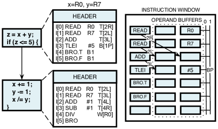
Figure 1 shows an example of two EDGE instruction blocks and how instructions explicitly encode their targets. In this example each block corresponds to a basic block. The first two READ instructions target the left (T[2L]) and right (T[2R]) operands of the ADD instruction. A READ is the only instruction that reads from the global register file (however any instruction may target, i.e. write to, the global register file). When the ADD receives the result of both register reads it will become ready and execute.
Figure 2 shows the general instruction format. Each EDGE instruction is 32 bits and supports encoding up to two target instructions. For instructions with more consumers than target fields, the compiler can build a fanout tree using move instructions or it can can assign high fanout instructions to broadcasts [15]. Broadcasts support sending an operand over a lightweight network to any number of consumer instructions in a block. In Figure 1, when the TLEI (test-less-than-equal-immediate) instruction receives its single input operand from the ADD it will become ready and execute. The test then produces a predicate operand that is broadcast on channel one (B[1P]) to all instructions listening on the broadcast channel, which in this example are the two predicated branch instructions (BRO.T and BRO.F). The branch that receives a matching predicate will fire.

A spectrum of EDGE implementations are possible with various area and performance tradeoffs. Prior EDGE research studied very wide issue implementations [12, 13], as well as fusion of multiple cores [14, 15, 16] to boost performance on scalar workloads. In this work we focus on MPPAA scenarios utilizing compact EDGE soft processors with competitive performance/area. Therefore data and pointers are 32 bits; blocks can be up to 32 instructions long; and the microarchitecture decodes 1-2 instructions per clock and issues one. We further restrict the load-store queue (LSQ) in this study to a simple, non-speculative design and omit branch or memory dependence prediction.
III EDGE in an FPGA
III-A Microarchitecture
Figure 3 is an example microarchitecure for a compact EDGE processor. It has much in common with a conventional in-order scalar RISC: instruction and data caches and a five stage pipeline including instruction fetch (IF), decode (DC), operand fetch, execute (EX), and memory/data cache access (LS). Unlike an in-order processor, instruction operands are read from operand buffers, not the register file; and the instruction to execute next, in dataflow order, is determined by the IS (issue) pipeline stage. This employs an instruction window comprising a dataflow instruction scheduler, a decoded instructions buffer, and operand buffers. It uses a simple load-store queue to issue memory instructions in program order.
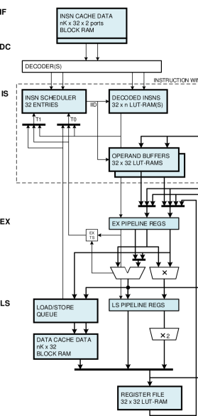
The front end (IF, DC) runs decoupled from the back end (IS, EX, LS). It fetches and decodes two instructions per clock into the instruction window. The instruction window’s dataflow scheduler keeps the ready state of each decoded instruction’s inputs i.e. its predication and operands. When all of its inputs (if any) are ready, the instruction wakes up and is ready to issue. The lowest numbered ready instruction IID is selected each cycle and its decoded instruction and input operands are read. Besides the data mux and function unit control signals, this instruction encodes up to two ready events. The scheduler accepts these and/or events from other sources (muxed into T0 and T1) and updates the ready state of other instructions in the window. Thus dataflow execution proceeds, starting with the block’s ready 0-input instructions, then instructions that these target, and so forth.
III-B EDGE dataflow instruction scheduling requirements
The instruction window and scheduler are the linchpin of the core. Their area, clock period, capabilities, and limitations largely determine the realized performance of an EDGE core and the throughput of an EDGE multiprocessor.
The instruction scheduler has diverse functionality and requirements. It is highly concurrent. Each cycle the decoder(s) write instructions’ decoded ready state and decoded instructions into the window. Each cycle the scheduler selects the next instruction to issue, and in response the back end sends ready events – either target ready events targeting a specific instruction’s input slot (predicate, operand #0, operand #1) or broadcast ready events targeting all instructions waiting on a broadcast ID. These set per-instruction active ready state bits which together with the decoded ready state may signal that the instruction is ready to issue. Note the scheduler sometimes accepts events for target instructions which have not yet been decoded and must also inhibit reissue of issued ready instructions.
EDGE instructions may be non-predicated, or predicated true or false. A predicated instruction does not become ready until it is targeted by another instruction’s predicate result, and that result matches the predicate condition. If the predicate doesn’t match, the instruction never issues.
On branch to a new block all instruction window ready state is flash cleared (block reset). However when a block branches back to itself (block refresh) only active ready state is cleared; the decoded ready state is preserved so that it is not necessary to re-fetch and decode the block’s instructions. Refresh is key to saving time and energy in loops.
Since some software critical paths consist of a single chain of dependent instructions, i.e. A targets B targets C, it is important that the dataflow scheduler add no pipeline bubbles for successive back-to-back instruction wakeup. Therefore the IS-stage ready-issue-target-ready pipeline recurrence should complete in one cycle – assuming this does not severely impact clock frequency.
Instructions such as ADD have a latency of one cycle. With EX-stage result forwarding the scheduler can wake their targets’ instructions in the IS-stage, even before the instruction completes. Other instruction results may await ALU comparisons, take multiple cycles, or have unknown latency. These must wait until later to wake their targets.
Finally, the scheduler design should be scalable across a spectrum of anticipated EDGE implementations – each cycle accepting at least 1-4 decoded instructions and 2-4 target ready events, and issuing 1-2 instructions per cycle.
We consider two alternative dataflow instruction scheduler designs: a brute-force parallel scheduler, where instructions’ ready state is explicily represented in FPGA D-flip-flops (FFs), in which the ready status of every instruction is reevaluated each cycle; and a more compact incremental scheduler which keeps ready state in LUT RAM and which updates ready status of only 2-4 target instructions per cycle.
III-C A parallel instruction scheduler
Figure 4 depicts a parallel instruction scheduler for the instruction window of Figure 3. Note the active ready state is set by target ready events T0, T1 and broadcast ID BID (if any), qualified by various input type enables ENs. For a 32-entry window there are 32 instances of a one-instruction ready circuit. In any cycle one or more of the 32 RDY signals may be asserted. A 32-bit priority encoder reduces this to the 5-bit IID of the next instruction to issue.
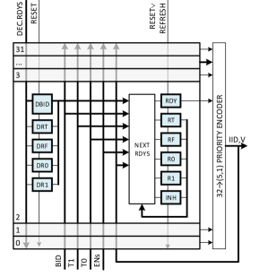
For each entry there are six bits of decoded ready state, i.e. they are initialized by the instruction decoder:
-
•
DBID: 2-bit binary broadcast ID, or 00 if none
-
•
DRT, DRF: decoder: predicate true (false) is ready
-
•
DR0, DR1: decoder: operand #0 (operand #1) is ready
Together these bits encode whether the instruction has been decoded, awaits a predicate and/or some operand(s), perhaps via a broadcast channel, or is immediately ready to issue. These bits are cleared on block reset only.
There are also six bits of active ready state:
-
•
RT, RF: predicate true (false) is ready
-
•
R0, R1: operand #0 (operand #1) is ready
-
•
INH: inhibit instruction – it has already issued
-
•
RDY: instruction is ready to issue
An instruction is ready iff (RT & RF & R0 & R1 & ~INH). Any of RT, RF, R0, R1 may be set when:
-
•
its corresponding DRX is set by the decoder, or
-
•
an executing instruction targets that input, explicitly, or via a broadcast event (broadcast ID, input).
Active ready state bits are cleared on block reset or refresh.
| Decoded ready state | Active ready state | ||||||||||
| Instruction | DBID | DRT | DRF | DR0 | DR1 | RT | RF | R0 | R1 | INH | RDY |
| READ | 00 | 1 | 1 | 1 | 1 | 1 | 1 | 1 | 1 | 1 | 0 |
| READ | 00 | 1 | 1 | 1 | 1 | 1 | 1 | 1 | 1 | 0 | 1 |
| ADD | 00 | 1 | 1 | 0 | 0 | 1 | 1 | 1 | 0 | 0 | 0 |
| TLEI | 00 | 1 | 1 | 0 | 1 | 1 | 1 | 0 | 1 | 0 | 0 |
| BRO.T B1 | 01 | 0 | 1 | 1 | 1 | 0 | 1 | 1 | 1 | 0 | 0 |
| BRO.F B1 | 01 | 1 | 0 | 1 | 1 | 1 | 0 | 1 | 1 | 0 | 0 |
| undecoded | 00 | 0 | 0 | x | x | 0 | 0 | x | x | x | 0 |
Table I depicts a block’s instruction scheduler state after decoding six instructions and issuing the first. The first four non-predicated instructions have DRT and DRF set reflecting that they do not await any particular predicate results. The two READ instructions, unpredicated and with zero input operands, are immediately ready to issue. The first has issued – and so is now inhibited from reissue – targeting operand 0 of the ADD, whose R0 is now set. The second READ will issue in the next IS pipeline cycle. The TLEI (test-less-than-or-equal-immediate) instruction broadcasts its predicate outcome on channel 1; the two branch instructions, predicated true (resp. false), await this predicate result. The seventh entry has not been decoded: (DRT|DRF)=0.
To reduce the critical path of dataflow scheduling, the front end writes predecoded EDGE instructions into the decoded instructions buffer. As instruction IID issues, its decoded instruction is read by the back end. Amongst other things it contains two target operand ready event fields, _T0 and _T1, which designate the 0-2 (IID, input) explicit targets of the instruction, as well as a 4-bit vector of input enables: ENs={RT_EN, RF_EN, R0_EN, R1_EN}. Referring back to Figure 3, these signals are muxed with ready events from other pipeline stages into T0 and T1 input by the scheduler.
III-D FPGA implementation of the parallel scheduler
Careful attention to FPGA circuit design is required to minimize the area and clock period of the scheduler. The 32-instruction window requires 32*(6+6)=384 FFs for the ready state, and 32*many LUTs to decode ready events and update each entry’s ready state.
A modern FPGA packs a set of LUTs (lookup tables) and D-flip-flops (FFs) together into a logic cluster. For example, Xilinx 7 series devices group four 6-LUTs and eight FFs into each “slice” cluster. Each LUT has two outputs and may be used as one 6-LUT, or two 5-LUTs with five common inputs. Each output may be registered in a FF. The flip-flops have optional CE (clock enable) and SR (set/reset) inputs but these signals are common to all eight FFs in the cluster. This basic cluster architecture is similar in Altera FPGAs.
From this follows two design considerations.
Fracturable 6-LUT decoders: For target instruction index decoding, so long as indices are 5 bits, two decoders may fit into a single 6-LUT.
Slice FF packing and cluster control set restrictions: To minimize area and wire delays, the design packs the ready state FFs densely, 4-8 FFs per cluster. Every 6-bit decoded ready state entry is written together (common RST and CE) and can pack into one or two slices.
More care is required for the active ready state FFs. Each of these 32*6=192 FFs may be individually set, but by packing four FFs per slice, when one FF is clock enabled, all are clock enabled. Whenever a FF is set by a ready event the other FFs in its slice should not change. This requires implementing CE functionality in each FF’s input LUT, feeding back its output into its input: FF_NXT = FF | (EN & input).
Listing 1 is Verilog that generates the “next readys“ for an N-entry parallel scheduler. Although there are four ready event input types (predicate true, false, operand #0, operand #1), by ensuring that predicate target events never occur in the same cycle as operand target events, a single target index bit suffices to distinguish false/operand #0 targets from true/operand #1 targets. (Further decoding is provided by specific {RT/RF/R0/R1}_ENs enables.) Therefore for an instruction window with N=32 entries, T0 and T1 are six bits {input#:1; IID:5}. The target decoders T00, T01, T10, T11 (target-0-input-0, etc.) are each one 6-LUT, as is the broadcast select decoder B. The next active ready state logic folds together the target decoder outputs with current active and decoded ready state. This requires another seven LUTs (two for INH_NXT), for a total of 32*12 = 384 LUTs.
This may be improved by splitting the 32-entry scheduler into two 16-entry banks of even and odd instructions. Within a bank a 4-bit bank-IID suffices. Then T0, T1 narrow to five bits so T00, T01, T10, T11 fit in two 5,5-LUTs, and INH_NXT in one 6-LUT, or 2*16*(3+6)=288 LUTs in all.
Besides shaving LUTs, a two bank scheduler provides two sets of T0, T1 ports and can sink two sets of two events each cycle. This is essential to sustain wider issue rates of two instructions per cycle (which may target four operands per cycle). Yet-wider issue and yet-larger instruction windows may even merit a four bank design.
The ready-issue-target-ready scheduling recurrence is the critical path of the IS-stage. A 325 priority encoder reduces the RDY vector to an IID which selects the decoded instruction. The decoded instruction’s fields {_T0,_T1,_BID,_ENs} are muxed into {T0,T1,BID,ENs} which update target instructions’ ready state, including RDY.
Priority encoder: Many 32-bit encoder designs were evaluated, including onehot conversion with LUT or carry-logic or-trees, carry-logic zero-scan, and F7MAP/F8MAP muxes. The present design uses two 164 encoders, one per bank, which complete in two LUT delays. In a one-issue processor, a subsequent 2:1 mux selects one of these encoder outputs.
In particular each 16-bit encoder input I[15:0] is chunked into I[15], I[14:10], I[9:5], I[4:0]. Each 5-bit group indexes a 32x4 LUT ROM with the precomputed encoder output for that group. Together with three 5-bit zero comparator outputs, these feed a custom 4-bit 3:1 selector which outputs ’b1111 when all three groups are zero.
Technology mapping and floorplanning: The design uses an RPM (relationally placed macro) methodology to improve area and interconnect delays and achieve a repeatable layout for easy routing and timing closure under module composition and massive replication. Structural RTL instantiates modules and tiles them into a scheduler. The XST annotation (*LUT_MAP=”yes”*) on a 6-input module locks its logic to one LUT; (*RLOC=”XxYy”*) packs FPGA primitives into clusters and places clusters relative to each other.

Figure 5 is a Xilinx 7-series implementation of Figure 4, including the scheduler, priority encoder, and decoded instruction buffer, with the critical path highlighted in white.
Each two horizontal rows of FPGA slices correspond to four entries in the instruction window. Left to right are:
-
•
pale yellow: four 6-bit decoded ready state flip-flops;
-
•
yellow/green: B, T00, T01, T10, T11 target decoders;
-
•
orange: active ready state LUTs/FFs RT_NXT/RT, etc.;
-
•
purple: INH_NXT and INH;
-
•
red: RDY_NXT and RDY.
To the right are the synthesized priority encoders and muxes (blue) and the decoded instructions buffer (white) implemented in several 32x6-bit true dual port LUT RAMs.
Performance: In a Kintex-7 -1-speed grade, the critical path takes 5.0 ns, including RDY clock-to-out, priority encoder, mux, decoded instructions LUT RAM, next readys logic and RDY setup. Interconnect delay is 85% of the critical path – unfortunately all paths from any RDY to any RDY must traverse a relatively large diameter netlist.
Cycle time may be reduced to 2.9 ns by adding a pipeline register halfway through the scheduler critical path (the output port of the instruction buffer LUT RAM) however this will not achieve back-to-back issue (in successive cycles) of a single dependent chain of instructions.
III-E Incremental dataflow scheduler ready state
The parallel scheduler is straightforward but it consumes hundreds of LUTs and FFs just to maintain 32x12b of ready state – a few LUTs worth of LUT RAM – and this area doubles as the instruction window size doubles. Also, each cycle its next readys LUTs recompute the readiness of every instruction, even though (broadcast notwithstanding) each issued instruction affects at most two others’ ready state. In contrast, the incremental scheduler keeps decoded and active ready state in LUT RAM, maintains the frontier of ready instructions in queues, and evaluates the ready status of just 2-4 target instructions per cycle. Compared to an array of FFs, LUT RAM is fast and dense but has some shortcomings: there is no way to flash clear it, and it only supports one write per cycle.
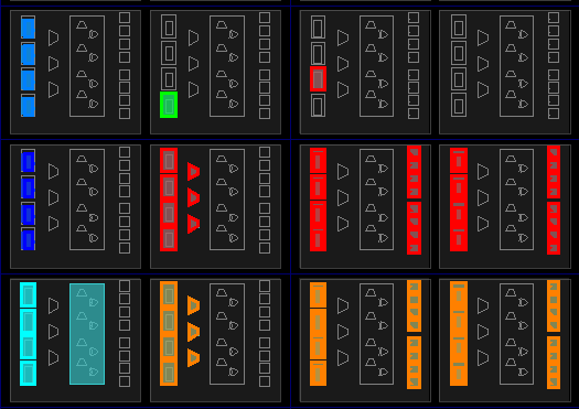
Instead, the scheduler uses a hybrid of LUT RAM and FF “RAM”. Decoded (DRT, DRF, DR0, DR1) and active (RT, RF, R0, R1) ready state are stored in several banks of 16x4 true dual port LUT RAM, which is validated by a 16x1 flash-clearable-set-only-RAM “FC-SO-RAM”. This comprises 16 FFs (with common reset), 16 write port address decoders (eight 5,5-LUTs), and a 16:1 read port mux (four 6-LUTs, two MUXF7s, one MUXF8) – just three slices in all. Each read from this hybrid reads the 4b LUT RAM entry and its valid bit. Each write updates the LUT RAM and sets its valid bit.
Multiple LUT RAM write ports. To sustain a fetch/decode rate of d instructions/cycle, and an issue rate of i instructions/cycle, it is necessary to update d+2i ready state entries each cycle. This is a challenge for one write/cycle LUT RAM. Rather than use clock doubling or replicated RAM banks with live value tables, the incremental scheduler divides the ready state up into four (or more) interleaved, disjoint banks: (decoded, active) ready state for (even, odd) instructions. Then the front end can write even and odd decoded ready state while the back end updates even and/or odd target instructions’ active ready state.
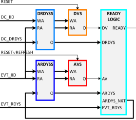
Figure 6 shows the resulting a 16-entry scheduler bank design and implementation. The blue decoded and active ready state LUT RAMs DRDYSS and ARDYSS are validated by orange/red FC-SO-RAMs DVS and AVS. Each cycle the decoder writes instruction DC_IID’s decoded ready state DC_DRDYS and its valid bit. Also each cycle the bank’s target ready event EVT ::={EVT_IID; EVT_RDYS} is processed via a read-modify-write of EVT_IID’s ARDYS with its DRDYS and EVT_RDYS. See Listing 2. The instruction is ready when all four ARDYS bits are set. All of this logic (cyan) requires just one slice; as an optimization READY’s and-reduction is in carry-logic.
Note that the EDGE compiler does not guarantee that both targets of an instruction are in disjoint banks so there may be scheduler bank conflicts. An ADD instruction might target an operand of instruction 10 and an operand of instruction 12. Since it is not possible to update the active ready state of the two even bank targets in the same cycle, one event is processed and the other is queued for a later cycle.
III-F Incremental dataflow scheduler design, operation, and implementation
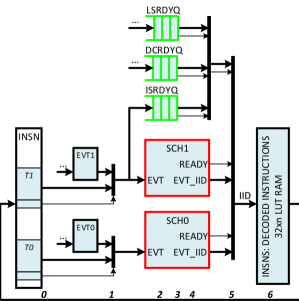
The core of the scheduler (Figure 7) consists of:
-
•
INSN: decoded instruction with two target event fields
-
•
EVT0, EVT1: even/odd pending event registers
-
•
even/odd event muxes, controlled by predecoded selects
-
•
SCH0, SCH1: even/odd 16-entry scheduler banks
-
•
three ready instruction IID queues:
-
–
DCRDYQ: decoder ready queue;
-
–
ISRDYQ: issue (scheduler) ready queue;
-
–
LSRDYQ: load/store ready queue
-
–
-
•
two 3:1 selectors to select next IID
-
•
INSNS: decoded instructions RAM (read port)
Note, in this design, the scheduler recurrence cycle begins and ends with the decoded instruction register.
Now consider execution of the first EDGE code block in Figure 1. The scheduler is reset, clearing DVS, AVS in SCH0, SCH1. The front end fetches the block’s header and fetches and decodes its instructions into INSNS. The two READs are ready to issue so their IIDs are enqueued on DCRDYQ. This “primes the pump” for the back end. The other instructions await operands or predicates, are not ready, so are not enqueued.
Back end dataflow execution proceeds as follows. Initially INSN is invalid and both READYs are negated. The IID selector tree selects/dequeues the first READ instruction (IID=0) from DCRDYQ. The decoded READ instruction word is read from INSNS into INSN.
The READ targets ADD operand #1. Its INSN.T0 (even bank target ready event) field is valid and its mux selects EVT=(2,’b0001) for SCH0. That updates ADD’s active ready state: ’b1100|’b0000|’b0001=’b1101, now awaiting only the left operand (operand #0). Since neither scheduler bank found a READY instruction, the IID selector tree selects/dequeues the second READ from DCRDYQ.
This READ targets ADD operand #0; its INSN.T0 is EVT=(2,’b0010). SCH0 updates ADD’s ready state to ’b1111 and asserts READY so the ADD (IID=2) issues.
ADD’s T1 targets the TLEI ready state in SCH1. TLEI becomes ready and issues.
As for TLEI, neither T0/T1 fields designate IS-stage ready events. Why? Unlike simple one cycle latency instructions like ADD, test instructions’ targets cannot receive ready events until the test executes in the EX-stage. Once a test completes, its true/false predicate event(s) are signaled. These proceed through queues and/or muxes (not shown) to the EVT0, EVT1 pending event registers, awaiting idle scheduler event slots.
Queues: The design employs many elastic FIFO ready queues and event queues. They are small and fast, built with up-down counters and Xilinx SRL32CE 32-bit variable length shift register LUTs. Besides DCRDYQ the present design has two other ready queues.
ISRDYQ: In a “one issue” design when an instruction issues and it targets and wakes two others, the even instruction issues next, and the odd one is queued on ISRDYQ.
LSRDYQ: EDGE processors use a load-store queue to provide sequential memory semantics. One simple area-optimized LSQ defers and reorders certain accesses; then when a (ready) load/store becomes issuable to memory the LSQ enqueues it on LSRDYQ.
Broadcast wakeup: Each EDGE result broadcast may target and wake an arbitrary number of instructions in the window. This is easy for a parallel scheduler but costly for an incremental one. When a result is broadcast the scheduler must sequentially update the ready state of every decoded instruction with that broadcast input. Therefore the decoder maintains queues (BR1Q, BR2Q, BR3Q) of IIDs of instructions with a given broadcast input. Once a broadcast result is known, the scheduler begins to dequeue the BRnQ IIDs into EVTs presented to SCH0, SCH1.
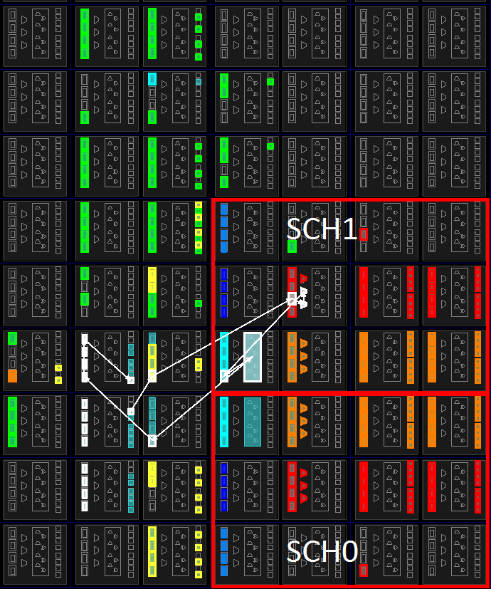
Performance: The labels 0-6 in Figure 7(a) depict the number of “LUT delays” to each point in the scheduler critical path, the white path in Figure 7(b). In a Kintex-7 -1-speed grade, this takes 4.3 ns including INSN clock-to-out, EVT mux, SCH1’s AVS read port mux, ARDYS_NXT and READY logic, IID selector, INSNS read, and INSN setup. Here interconnect delay is just 70% of the critical path reflecting relatively shorter nets and some use of LUT-local MUXF7/MUXF8/CARRY4 nets. The scheduler clock period may be reduced to 2.5 ns by adding pipeline registers after the LUT RAM and FC-SO-RAM reads, but as with the parallel scheduler, pipelining precludes back-to-back issue of dependent instructions.
III-G Comparing parallel and incremental schedulers
| Metric | Parallel | Incremental | Units |
| Area, 32 entries | 288 | 78 | LUTs |
| Area, total, 32 entries | 340 | 150 | LUTs |
| Period | 5.0 | 4.3 | ns |
| Period, pipelined | 2.9 | 2.5 | ns |
| Area, total * period | 1700 | 645 | LUT*ns |
| Broadcast | flash | iterative | |
| Event bank conflicts? | never | sometimes | |
| Area, 4 events/cycle | 288 | 156 | LUTs |
| Area, 64 entries | 576 | 130 | LUTs |
Table II summarizes the differences between the two dataflow scheduler designs. The core of the incremental scheduler is less than a third the size of the parallel scheduler although the size advantage is smaller when the additional overhead of queues and muxes is added. The incremental scheduler is also faster and the area*period metric is 2.6x better. However the parallel scheduler retains some brute force advantages. It can process a broadcast event in a single cycle, whereas the incremental scheduler must iteratively drain a broadcast queue at a rate of 1-2 instructions per cycle. This may cause issue stalls in some workloads. The incremental scheduler is also subject to even/odd target bank conflicts which may delay an instruction wake up. Real workload studies are needed to measure whether these effects overshadow its substantial area*period advantage.
Finally consider future scale up to wider issue and larger instruction windows. The parallel scheduler does not grow when subdivided into more banks to process twice as many events per cycle, whereas the incremental scheduler core area doubles. To grow the instruction window to 64 entries, the parallel scheduler require twice as much area, whereas the incremental scheduler area grows more modestly.
IV Conclusion
This paper presents our work towards a practical out-of-order dataflow soft processor architecture for FPGAs. We set out to discover whether a novel EDGE instruction set architecture, optimized for simpler high ILP microarchitectures in ASICs, is also a good fit for FPGAs, or whether general purpose soft processors will remain stuck in the scalar RISC slow lane.
We considered two different dataflow instruction scheduler designs and their optimized FPGA implementations. In the context of commercial 200 MHz, 1,000-2,000 LUT soft processors, the limited FPGA resource cost and clock period impact of either design seems acceptable and practical. Both design alternatives will scale well to future four-decode/two-issue implementations.
References
- [1] J. Gray, “Homebrewing RISCs in FPGAs,” http://fpgacpu.org/papers/j32.ppt, August 1996.
- [2] ——, “Building a RISC System in an FPGA,” Circuit Cellar Ink, no. 116–118, March, April, May 2000. [Online]. Available: http://fpgacpu.org/papers/xsoc-series-drafts.pdf
- [3] Altera Corporation, “Nios Embedded Processor Software Development Reference Manual,” March 2001.
- [4] Xilinx Inc., “MicroBlaze Processor Reference Guide,” 2002.
- [5] A. K. Jones, R. Hoare, D. Kusic, J. Fazekas, and J. Foster, “An FPGA-based VLIW Processor with Custom Hardware Execution,” in Proceedings of the 13th International Symposium on Field-programmable Gate Arrays, 2005, pp. 107–117.
- [6] K. O. I. Tili and J. G. Steffan, “TILT: A Multithreaded VLIW Soft Processor Family,” in Proceedings of the International Conference on Field Programmable Logic and Applications, August 2013.
- [7] P. Yiannacouras, J. G. Steffan, and J. Rose, “VESPA: Portable, Scalable, and Flexible FPGA-based Vector Processors,” in Proceedings of the International Conference on Compilers, Architectures and Synthesis for Embedded Systems, 2008, pp. 61–70.
- [8] J. Yu, G. Lemieux, and C. Eagleston, “Vector Processing As a Soft-core CPU Accelerator,” in Proceedings of the 16th International ACM/SIGDA Symposium on Field Programmable Gate Arrays, 2008, pp. 222–232.
- [9] R. Carli, “Flexible MIPS Soft Processor Architecture,” Master’s thesis, Massachusetts Institute of Technology, May 2008.
- [10] K. Aasaraai and A. Moshovos, “Towards a viable out-of-order soft core: Copy-free, checkpointed register renaming,” in Proceedings of the 19th International Conference on Field Programmable Logic and Applications, August 2009.
- [11] B. H. Dwiel, N. K. Choudhary, and E. Rotenberg, “FPGA Modeling of Diverse Superscalar Processors,” in Proceedings of the IEEE International Symposium on Performance Analysis of Systems and Software, 2012, pp. 188–199.
- [12] D. Burger, S. W. Keckler, K. S. McKinley, M. Dahlin, L. K. John, C. Lin, C. R. Moore, J. Burrill, R. G. McDonald, W. Yoder, X. Chen, R. Desikan, S. Drolia, J. Gibson, M. S. S. Govindan, P. Gratz, H. Hanson, C. Kim, S. K. Kushwaha, H. Liu, R. Nagarajan, N. Ranganathan, E. Reeber, K. Sankaralingam, S. Sethumadhavan, P. Sivakumar, and A. Smith, “Scaling to the End of Silicon with EDGE architectures,” IEEE Computer, vol. 37, no. 7, pp. 44–55, July 2004.
- [13] M. Gebhart, B. A. Maher, K. E. Coons, J. Diamond, P. Gratz, M. Marino, N. Ranganathan, B. Robatmili, A. Smith, J. Burrill, S. W. Keckler, D. Burger, and K. S. McKinley, “An Evaluation of the TRIPS Computer System,” in Proceedings of the 14th International Conference on Architectural Support for Programming Languages and Operating Systems, 2009, pp. 1–12.
- [14] C. Kim, S. Sethumadhavan, M. S. Govindan, N. Ranganathan, D. Gulati, D. Burger, and S. W. Keckler, “Composable lightweight processors,” in Proceedings of the 40th International Symposium on Microarchitecture, 2007, pp. 381–394.
- [15] B. Robatmili, D. Li, H. Esmaeilzadeh, S. Govindan, A. Smith, A. Putnam, D. Burger, and S. W. Keckler, “How to Implement Effective Prediction and Forwarding for Fusable Dynamic Multicore Architectures,” in Proceedings of the 19th International Symposium on High Performance Computer Architecture, 2013, pp. 460–471.
- [16] M. S. S. Govindan, B. Robatmili, D. Li, B. Maher, A. Smith, S. W. Keckler, and D. Burger, “Scaling power and performance via processor composability,” IEEE Transactions on Computers, March 2013.