Inverse Design of Compact Multimode Cavity Couplers
Abstract
Efficient coupling between on-chip sources and cavities plays a key role in silicon photonics. However, despite the importance of this basic functionality, there are few systematic design tools to simultaneously control coupling between multiple modes in a compact resonator and a single waveguide. Here, we propose a large-scale adjoint optimization approach to produce wavelength-scale waveguide–cavity couplers operating over tunable and broad frequency bands. We numerically demonstrate couplers discovered by this method that can achieve critical, or nearly critical, coupling between multi-ring cavities and a single waveguide at up to six widely separated wavelengths spanning the – nm range of interest for on-chip nonlinear optical devices.
Practical limitations of nanophotonics for broadband applications are seldom known and highly context specific Yu (2010); Miller et al. (2015); Arabi and Faraon (2017). In single frequency problems, traditional design principles based on index-guiding, Bragg scattering, and material resonances offer clear trade offs, e.g., spatial confinement for radiative losses, or peak performance for bandwidth. But, in many multi-frequency problems, including nonlinear optics Sitawarin et al. (2017); Li et al. (2016), imaging Sell et al. (2017); Callewaert et al. (2018), radiative heat transfer Jin et al. (2017, 2018), and optical networks Miller (2017), the number of parameters that influence performance is simply too large to treat completely using analytic methods or hand-designed geometries, and it is often unclear what level of performance can be attained. Over the last two decades, this challenge has spurred the development of large-scale optimization (inverse) techniques to assist in the design process with promising early returns Jensen and Sigmund (2011); Lu and Vučković (2013); Lalau-Keraly et al. (2013). Yet, in many technically important areas only preliminary investigations have been made Molesky et al. (2018). Specifically, the power required to attain efficient nonlinear frequency conversion processes is known to decrease with increasing spatial confinement, so long as the overlap of the participating modes can be controlled Rodriguez et al. (2007). To take full advantage of this effect, we have recently proposed several optimized resonators to enhance nonlinear second harmonic and difference frequency generation in wavelength-scale volumes Lin et al. (2016, 2017a). To operate on-chip, each mode in a device making use of these cavities must be coupled to a source or detector in a controlled way; and until presently, we have not addressed how this can be done. Using a typical evanescent scheme, tuning the gap separation to control evanescent overlap between the waveguide and cavity Chandrahalim et al. (2017), realization of high efficiency devices using these cavities, and similar future designs, may be difficult. Beyond the issues of layout intricacy, bending loss Vlasov and McNab (2004); Fujisawa et al. (2017), and waveguide crosstalk Donzella et al. (2013); Jahani and Jacob (2015) that would be introduced by requiring multiple waveguides to intersect in a wavelength-scale area, modes in the best performing cavities designs may be tightly confined to the core Lin et al. (2017a), precluding the possibility of achieving critical or over coupling by simply decreasing the separation.
This problem of efficiently coupling light between sources and predefined volumes appears in many branches of nanophotonics. For instance, it is the defining goal of wide-area absorbers—surfaces that can perfectly absorb a wide range of incident propagating waves. Broadly, the main approach in this setting is to create structures supporting many resonances in order to tune the radiative and absorptive decay rates in each scattering channelGhebrebrhan et al. (2011). This behaviour can be introduced in a wide variety of ways, including adiabatic tapers Wu (2016); Lin et al. (2017b), metasurfaces Argyropoulos et al. (2013); Liu et al. (2017), epsilon-near-zero thin films Molesky et al. (2013); Rensberg et al. (2017), chirped gratings Song et al. (2013); Ji et al. (2014), multi-resonant photonic crystals Rinnerbauer et al. (2014), and more recently, unintuitive structures obtained via inverse design Ganapati et al. (2014); Sui et al. (2015); Fu et al. (2016). A similar objective also appears in the context of free-space to on-chip couplers, with the primary aim being to reduce losses, i.e. reflections, of light incident on a on-chip device from either a fiber or free space. Rate matching is more difficult to implement in these situations, as any signal decay (e.g. material absorption in the coupling region) reduces performance; and common approaches based on adiabatic tapers lead to couplers that are several wavelengths long and are only typically designed to operate over narrow, selective bands Almeida et al. (2003); Carmon et al. (2007); Fu et al. (2014); Tiecke et al. (2015). Based on motivations similar to those of this present study, there is a current push to exploit inverse design Niederberger et al. (2014); Mansoor et al. (2017), metasurface concepts Zhu et al. (2017); Li et al. (2017, 2018), and chaotic deformations Jiang et al. (2017) in this area. Likewise, a need to control coupling arises between on-chip devices, including filters, rectifiers, multiplexers, and frequency converters. In these situations, the usual goal is to efficiently couple two or more separately designed devices in the smallest possible footprint. Again, much in the spirit of the results presented here, within the past few years inverse design approaches have started to be applied in this setting, leading to experimental demonstrations of compact wavelength-division mulitplexers operating over several far-apart wavelengths Piggott et al. (2015); Frellsen et al. (2016).
In this paper, we present a large-scale optimization algorithm for designing compact on-chip devices that efficiently couple light consisting of multiple, widely separated wavelengths from a single waveguide into a wavelength-scale multi-resonant cavity. Motivated by practical problems in nonlinear optics, we pursue three illustrative examples: compact multi-resonant cavities with resonant features mimicking those used for second-harmonic, sum-frequency, and frequency comb generation. In each situations, we demonstrate either total or near total critical coupling.
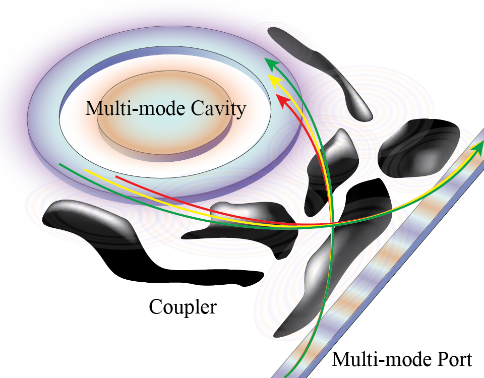
Formulation.— Our conception of the coupling problem is depicted in Fig. 1. Starting from an isolated cavity supporting resonances with frequencies and radiative lifetimes , , we aim to design a wavelength-scale device that tunes the external coupling rate of each mode to a single nearby waveguide to any desired value. That is, we seek to independently control the dimensionless coupling quality factor of every individual mode of a given set. Generically, the presence of a coupler or a nearby waveguide can significantly alter the radiative decay of an isolated cavity modes, either enhancing or degrading temporal confinement. To ensure that the resonant features of the cavity are not destroyed by the coupler, we simultaneously constrain , with denoting the radiative quality factor of the cavity in the presence of the waveguide and coupler, and an adjustable scale factor. Based on this description, a structure for any desired collection of coupling characteristics is discoverable using a gradient adjoint-variable topology optimization approach Liang and Johnson (2013) that seeks to solve the minimax problem,
| (1) | ||||
| s.t. | ||||
where
| (2) | |||
with denoting the target ratio of . In this method, the dielectric permittivity at every spatial point inside the coupling region, , is as a continuous degree of freedom, bounded by the substrate and structure materials. (To produce binary, smooth, fabricable systems additional regularization and filter projection steps are applied in conjunction with this base algorithm Wang et al. (2011).) In order to circumvent numerical issues associated with optimizations of electromagnetic eigenvalues Liang and Johnson (2013), each is computed by solving a set of scattering problems. This makes both the objective and constraints explicit functions of the electric field , computed as the solution of the steady-state equation . To setup this problem, electric current sources, the duals of the modes in the energy norm Chembo and Yu (2010), are first calculated (without the waveguide and coupler) at each individual frequency. The waveguide and coupler are then added, and the field quantities of interest determined: the electromagnetic energy density inside the cavity volume, , and the Poynting flux into the waveguide and radiated into vacuum, , with denoting the corresponding flux surfaces. The radiative and coupling lifetimes are then used to evaluate and .
In many applications of interest, one of two coupling characteristics are often desired: over coupling Guo et al. (2016); Pfeiffer et al. (2017), minimizing unwanted losses and increasing energy efficiency, or critical coupling, maximizing field amplitudes in the cavity Lin et al. (2016). For cavities designed to enhance nonlinear frequency conversion, such as the illustrative examples considered below, maximum power conversion occurs under critical coupling, , at each frequency. In such cases, the general scheme presented above can be simplified. When the cavity is pumped from a single channel with power , the energy in the cavity is related to the quality factors by Suh et al. (2004)
| (3) |
reaching a relative maximum of as the system moves toward critical coupling (). Technically, (3) is only applicable to unidirectional couplers, i.e. when each cavity mode couples only to one port (direction) of the waveguide. (A simple example of a unidirectional coupler is the usual waveguide–ring resonator system, where the direction of coupling is constrained by momentum conservation Gorodetsky and Ilchenko (1999).) However, as the introduction of any additional coupling channel always reduces the energy stored in the cavity Suh et al. (2004), in practice, there is no loss of generality in considering this expression. By maximizing the energy in the cavity, the algorithm naturally proceeds towards unidirectional couplers, which in turn makes (3) an increasingly good approximation. Since the behavior of (3) is then ultimately equivalent to the more complicated (2), we are able to consider the simpler optimization problem,
| (4) |
Where the is an energy normalization factor given by the bare radiative lifetime.
As a proof of concept, we consider two illustrative cavities designed to enhance two nonlinear processes: up-conversion of and to the summed frequency (SFG), and second-harmonic generation (SHG) corresponding to degenerate SFG with . For these processes, the relative coupling rates largely dictate the achievable intensities in the cavity, and hence power requirements (in the undepleted regime Lin et al. (2016)). Mathematically, this is captured by the figure of merit
| (5) |
with denoting the overlap coefficient of the cavity fields, which to first order is not affected by the external waveguide or coupler. Like (3), (5) is maximized when all three modes achieve critical coupling, giving .
Results.— As a platform for testing our algorithm, similar to proposed wavelength-scale cavities for implementing nonlinear phenomenaLin et al. (2017a), we consider a two-dimensional system consisting of hand-designed multi-track ring-resonators supporting TM-polarized resonances of moderate radiative lifetimes , and a rectangular admissible coupler region covering the separation between the cavity and the waveguide. The size of this design region is determined on a case-by-case basis as a compromise between compactness and functionality. Starting from a base of 3.75 m 1.5 m the size of the coupling region is increased whenever the algorithm is unable to find suitable coupling structures. To guide the algorithm towards more easily fabricable structures, the coupler is always seeded with connected, smooth dielectric profiles, i.e. a random ribbon. (For numerical accuracy, the grid resolution is chosen to be smaller than for the smallest wavelength considered, pixels per wavelength inside the highest index media.)
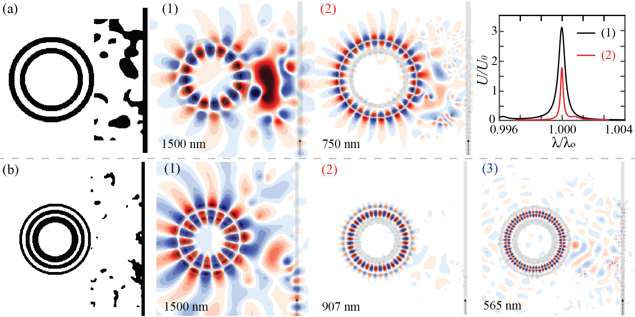
Our findings begin with the SHG and SFG systems depicted Fig. 2. For practical considerations, these simulations suppose a gallium phosphide material (including material dispersion) for all dielectric regions: the cavity, waveguide, and coupler. The initial SHG system is a two-track multi-ring supporting TM-polarized resonances at nm, quality factors of , with power coupled into the device through a narrow waveguide at a gap separation of 1.5. (The azimuthal numbers of these modes satisfy the phase-matching condition for the (111) plane of a GaP crystal. Given a different nonlinear tensor and requisite polarizations, the phase-matching condition for can be slightly different Bi et al. (2012).) As indicated in the field profiles of Fig. 2 (a), in the presence of the coupler each mode shows vanishing transmission and reflection (), and large field amplitude inside the cavity. Quantitatively, Fig. 2 (a) (rightmost) examines the energy spectrum inside the resonator channeled from the waveguide around , normalized by . After optimization, the cavity mode lifetime is more than doubled, with . As expected, eigenmode analysis reveals the system to be totally asymmetric, with the cavity coupling exclusively to the lower waveguide (downwards propagation). The coupler is also observed to be both binary and smooth, having no feature smaller than nm. Nearly identical results are seen for the triply resonant system (non-degenerate SFG) illustrated in Fig. 2 (b). Moving to a three-track cavity designed to support modes at nm, with , the algorithm is again able to realize critical coupling at all three wavelengths, resulting in transmission . Cavity radiative lifetimes are also similarly enhanced, with . In either inverse design, the coupling mechanism is found to be more intricate than just the overlap of evanescent fields used for single wavelengths. This is most pointedly seen in (2) and (3) of Fig.2 (b), where over % of the energy density is in the cavity, yet critical coupling occurs at over two wavelength of separation due to the fields in the coupler. Moreover, for some cavity modes, even at a single wavelength, it would not be possible to achieve critical coupling using the evanescent tails of a waveguide mode. For example, due to its tight confinement to the inner ring, even if the waveguide is made to touch the cavity, it is not possible to couple to the mode displayed in Fig. 2 (a.1) with better than efficiency. (Reducing the waveguide cross-section offers no improvement due to the creation of phase mismatch.) Note that the radiative quality factors of the cavities we have designed are smaller than those typically considered for nonlinear processes. This choice was made primarily to test the algorithm in cases involving dissimilar waveguide and cavity mode profiles Xu et al. (2008). Nevertheless, we note that for equivalent nonlinear performance, larger overlaps and smaller radiative lifetimes are often preferable to higher quality factors Lin et al. (2016).
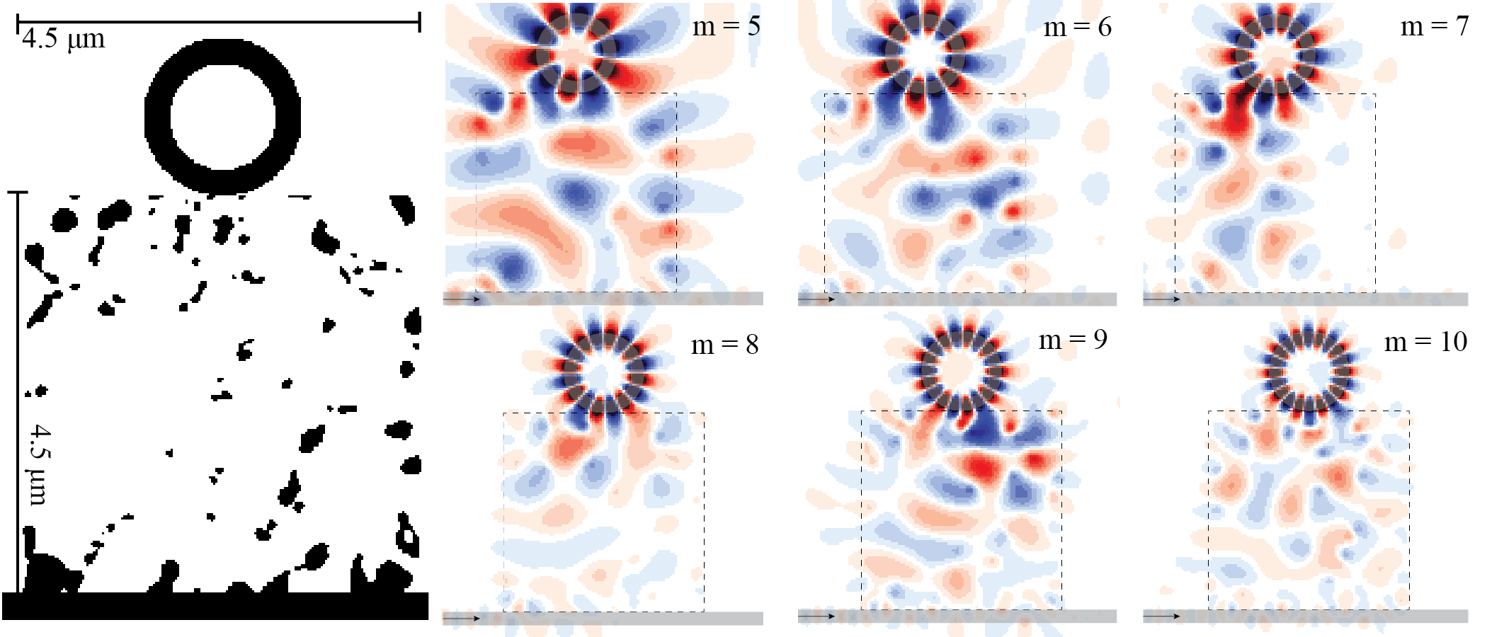
As a final benchmark, Fig. 3 demonstrates a system attaining near critical coupling at 6 frequencies (over an octave), a frequency comb with large tooth spacing. (A more practical frequency comb coupler, e.g. exhibiting critical coupling at over frequencies, will be considered in future work.) In this case, we begin with a wavelength-scale ring resonator having unevenly distributed modes at intervals m, with . To simplify future comparisons, material dispersion is ignored and the cavity, waveguide and coupler are all assumed to have a constant permittivity of . As opposed to our first two examples, where the modal resonance frequencies are fixed constraints, adding a degree of modularity to the total system design, here, we assume that the resonance frequencies must be tuned by the coupler. This conceptual shift requires some small modifications to stabilize the optimization algorithm. Namely, we now include an initial phase where the usual energy density objectives are replaced by field overlap integrals with the eigenmodes of the cavity , where the subscript denotes the mode of the bare cavity, and, as before, the integration is restricted to lie within the outermost material boundary of the cavity. The frequencies where these computations are carried out are initialized to match those of the bare cavity, and then slowly transitioned to the desired resonances, i.e. an evenly distributed set. The converged output of this procedure is effectively a new cavity having characteristics well-matched to the original coupling optimization algorithm. The coupler displayed in Fig. 3 achieves the desired wavelength tuning and critical-coupling functionality. The resonance frequency intervals are equally distributed as m, and good coupling (transmission and reflection below ) is visibly present in each of the field profile plots. Explicitly, the summed transmitted and reflected powers of are found to be . However, smaller minimal feature sizes, nm, and a larger total footprint were required to achieve these effects. The number of iterations needed for this optimization was roughly the same as those of the previous examples, leading to approximately linearly scaling of the total computation time with the number of frequencies.
In summary, we have shown that, in two dimensions, inverse design provides a practical means of efficiently coupling light at multiple widely separated wavelengths from a single channel (a waveguide) into a compact, multimode cavity. Drawing from our recent work on the design of compact microcavities for high-efficiency nonlinear frequency conversion, we have successfully treated suggestive examples for second-harmonic (SHG), sum-frequency (SFG), and frequency comb generation (albeit for large tooth spacing). Critical coupling was achieved, or nearly achieved, at all relevant wavelengths without incorporating sharp components in the first two cases. In particular, all features of the SHG system are larger than nm. Our results continue the promising trend seen in application of inverse design to free-space and on-chip couplers, rectifiers, and multiplexers, indicating the potential of these techniques to enable significant improvements in integrated nonlinear photonics.
Acknowledgments.— This work was supported by the National Science Foundation under Grant No. DMR-1454836, Grant No. DMR 1420541, and Award EFMA-1640986; and the National Science and Research Council of Canada under PDF-502958-2017.
References
- Yu (2010) Z. Yu, Proceedings of the National Academy of Sciences 107, 17491 (2010).
- Miller et al. (2015) O. D. Miller, S. G. Johnson, and A. W. Rodriguez, Physical Review Letters 115, 204302 (2015).
- Arabi and Faraon (2017) A. Arabi and A. Faraon, Scientific Reports 7 (2017).
- Sitawarin et al. (2017) C. Sitawarin, W. Jin, Z. Lin, and A. W. Rodriguez, arXiv:1711.07810 (2017).
- Li et al. (2016) Q. Li, M. Davanço, and K. Srinivasan, Nature Photonics 10, 406 (2016).
- Sell et al. (2017) D. Sell, J. Yang, S. Doshay, R. Yang, and J. A. Fan, Nano Letters 17, 3752 (2017).
- Callewaert et al. (2018) F. Callewaert, V. Velev, P. Kumar, A. Sahakian, and K. Aydin, Scientific Reports 8, 1358 (2018).
- Jin et al. (2017) W. Jin, R. Messina, and A. W. Rodriguez, Optics Express 25, 14746 (2017).
- Jin et al. (2018) W. Jin, S. Molesky, Z. Lin, and A. W. Rodriguez, arXiv:1802.05744 (2018).
- Miller (2017) D. A. Miller, Nature Photonics 11, 403 (2017).
- Jensen and Sigmund (2011) J. S. Jensen and O. Sigmund, Laser & Photonics Reviews 5, 308 (2011).
- Lu and Vučković (2013) J. Lu and J. Vučković, Optics Express 21, 13351 (2013).
- Lalau-Keraly et al. (2013) C. M. Lalau-Keraly, S. Bhargava, O. D. Miller, and E. Yablonovitch, Optics Express 21, 21693 (2013).
- Molesky et al. (2018) S. Molesky, Z. Lin, A. Y. Piggott, W. Jin, J. Vuckovic, and A. W. Rodriguez, arXiv:1801.06715 (2018).
- Rodriguez et al. (2007) A. Rodriguez, M. Soljačić, J. D. Joannopoulos, and S. G. Johnson, Optics express 15, 7303 (2007).
- Lin et al. (2016) Z. Lin, X. Liang, M. Lončar, S. G. Johnson, and A. W. Rodriguez, Optica 3, 233 (2016).
- Lin et al. (2017a) Z. Lin, M. Lončar, and A. W. Rodriguez, Optics Letters 42, 2818 (2017a).
- Chandrahalim et al. (2017) H. Chandrahalim, S. C. Rand, and X. Fan, Applied Optics 56, 4750 (2017).
- Vlasov and McNab (2004) Y. A. Vlasov and S. J. McNab, Optics express 12, 1622 (2004).
- Fujisawa et al. (2017) T. Fujisawa, S. Makino, T. Sato, and K. Saitoh, Optics Express 25, 9150 (2017).
- Donzella et al. (2013) V. Donzella, S. T. Fard, and L. Chrostowski, in Photonics North 2013, Vol. 8915 (International Society for Optics and Photonics, 2013) p. 89150Z.
- Jahani and Jacob (2015) S. Jahani and Z. Jacob, JOSA B 32, 1346 (2015).
- Ghebrebrhan et al. (2011) M. Ghebrebrhan, P. Bermel, Y. Yeng, I. Celanovic, M. Soljačić, and J. Joannopoulos, Physical Review A 83, 033810 (2011).
- Wu (2016) J. Wu, Optics Communications 365, 93 (2016).
- Lin et al. (2017b) Y. Lin, Y. Cui, F. Ding, K. H. Fung, T. Ji, D. Li, and Y. Hao, Optical Materials Express 7, 606 (2017b).
- Argyropoulos et al. (2013) C. Argyropoulos, K. Q. Le, N. Mattiucci, G. D’Aguanno, and A. Alu, Physical Review B 87, 205112 (2013).
- Liu et al. (2017) X. Liu, K. Fan, I. V. Shadrivov, and W. J. Padilla, Optics Express 25, 191 (2017).
- Molesky et al. (2013) S. Molesky, C. J. Dewalt, and Z. Jacob, Optics Express 21, A96 (2013).
- Rensberg et al. (2017) J. Rensberg, Y. Zhou, S. Richter, C. Wan, S. Zhang, P. Schöppe, R. Schmidt-Grund, S. Ramanathan, F. Capasso, M. A. Kats, et al., Physical Review Applied 8, 014009 (2017).
- Song et al. (2013) Y. Song, C. Wang, Y. Lou, B. Cao, and X. Li, Optics Communications 305, 212 (2013).
- Ji et al. (2014) D. Ji, H. Song, X. Zeng, H. Hu, K. Liu, N. Zhang, and Q. Gan, Scientific Reports 4, 4498 (2014).
- Rinnerbauer et al. (2014) V. Rinnerbauer, Y. Shen, J. D. Joannopoulos, M. Soljačić, F. Schäffler, and I. Celanovic, Optics Express 22, A1895 (2014).
- Ganapati et al. (2014) V. Ganapati, O. D. Miller, and E. Yablonovitch, IEEE Journal of Photovoltaics 4, 175 (2014).
- Sui et al. (2015) S. Sui, H. Ma, J. Wang, Y. Pang, and S. Qu, Journal of Physics D: Applied Physics 48, 215101 (2015).
- Fu et al. (2016) S. M. Fu, Y. K. Zhong, N. P. Ju, M.-H. Tu, B.-R. Chen, and A. Lin, IEEE Photonics Journal 8, 1 (2016).
- Almeida et al. (2003) V. R. Almeida, R. R. Panepucci, and M. Lipson, Optics Letters 28, 1302 (2003).
- Carmon et al. (2007) T. Carmon, S. Y. Wang, E. P. Ostby, and K. J. Vahala, Optics Express 15, 7677 (2007).
- Fu et al. (2014) Y. Fu, T. Ye, W. Tang, and T. Chu, Photonics Research 2, A41 (2014).
- Tiecke et al. (2015) T. Tiecke, K. Nayak, J. Thompson, T. Peyronel, N. De Leon, V. Vuletić, and M. Lukin, Optica 2, 70 (2015).
- Niederberger et al. (2014) A. C. Niederberger, D. A. Fattal, N. R. Gauger, S. Fan, and R. G. Beausoleil, Optics Express 22, 12971 (2014).
- Mansoor et al. (2017) R. Mansoor, H. Sasse, and A. Duffy, International Journal of Numerical Modelling: Electronic Networks, Devices and Fields 30 (2017).
- Zhu et al. (2017) L. Zhu, W. Yang, and C. Chang-Hasnain, Optics Express 25, 18462 (2017).
- Li et al. (2017) Z. Li, M.-H. Kim, C. Wang, Z. Han, S. Shrestha, A. C. Overvig, M. Lu, A. Stein, A. M. Agarwal, M. Lončar, et al., Nature Nanotechnology 12, 675 (2017).
- Li et al. (2018) J. Li, Y. Liu, Y. Meng, K. Xu, J. Du, F. Wang, Z. He, and Q. Song, IEEE Photonics Technology Letters (2018).
- Jiang et al. (2017) X. Jiang, L. Shao, S.-X. Zhang, X. Yi, J. Wiersig, L. Wang, Q. Gong, M. Lončar, L. Yang, and Y.-F. Xiao, Science 358, 344 (2017).
- Piggott et al. (2015) A. Y. Piggott, J. Lu, K. G. Lagoudakis, J. Petykiewicz, T. M. Babinec, and J. Vučković, Nature Photonics 9, 374 (2015).
- Frellsen et al. (2016) L. F. Frellsen, Y. Ding, O. Sigmund, and L. H. Frandsen, Optics Express 24, 16866 (2016).
- Liang and Johnson (2013) X. Liang and S. G. Johnson, Optics Express 21, 30812 (2013).
- Wang et al. (2011) F. Wang, B. S. Lazarov, and O. Sigmund, Structural and Multidisciplinary Optimization 43, 767 (2011).
- Chembo and Yu (2010) Y. K. Chembo and N. Yu, Physical Review A 82, 033801 (2010).
- Guo et al. (2016) X. Guo, C.-L. Zou, H. Jung, and H. X. Tang, Physical Review Letters 117, 123902 (2016).
- Pfeiffer et al. (2017) M. H. Pfeiffer, J. Liu, M. Geiselmann, and T. J. Kippenberg, Physical Review Applied 7, 024026 (2017).
- Suh et al. (2004) W. Suh, Z. Wang, and S. Fan, IEEE Journal of Quantum Electronics 40, 1511 (2004).
- Gorodetsky and Ilchenko (1999) M. L. Gorodetsky and V. S. Ilchenko, JOSA B 16, 147 (1999).
- Bi et al. (2012) Z.-F. Bi, A. W. Rodriguez, H. Hashemi, D. Duchesne, M. Loncar, K.-M. Wang, and S. G. Johnson, Optics Express 20, 7526 (2012).
- Xu et al. (2008) Q. Xu, D. Fattal, and R. G. Beausoleil, Optics Express 16, 4309 (2008).