The energy scale of Dirac electrons in Cd3As2
Abstract
Cadmium arsenide (Cd3As2) has recently became conspicuous in solid-state physics due to several reports proposing that it hosts a pair of symmetry-protected 3D Dirac cones. Despite vast investigations, a solid experimental insight into the band structure of this material is still missing. Here we fill one of the existing gaps in our understanding of Cd3As2, and based on our Landau level spectroscopy study, we provide an estimate for the energy scale of 3D Dirac electrons in this system. We find that the appearance of such charge carriers is limited – contrary to a widespread belief in the solid-state community – to a relatively small energy scale (below 40 meV).
pacs:
78.20.Ls, 71.28.+d, 71.70.DiI Introduction
The presence of three-dimensional (3D) massless Dirac electrons in cadmium arsenide (Cd3As2) is nowadays taken as granted, from both experimental and theoretical point of views.Wang et al. (2013); Borisenko et al. (2014); Neupane et al. (2014); Liu et al. (2014) Cd3As2 is thus often cited as the first identified symmetry-protected 3D Dirac semimetal that is stable under ambient conditions. The cartoon picture of its band structure – with two Dirac cones located along the tetragonal axis – is even viewed as a textbook example for this class of materials.
In reality, the band structure of Cd3As2 is far more complex and the presence of Dirac electrons, which are of key interest in this material,Wang et al. (2013) is not proven. The broadly extended conical band reported in recent experiments on Cd3As2Borisenko et al. (2014); Neupane et al. (2014); Liu et al. (2014) is most likely not related to any Dirac physics.Jeon et al. (2014); Akrap et al. (2016) Instead, this conical band seems to be a simple consequence of a vanishing band gap in the material studied. The low-energy electronic states – where a pair of truly Dirac cones may indeed be expectedWang et al. (2013); Conte et al. (2017) – have been so far barely addressed in experiments. Hence, at present, the Dirac electrons in Cd3As2 do not represent more than an appealing theoretical construct.
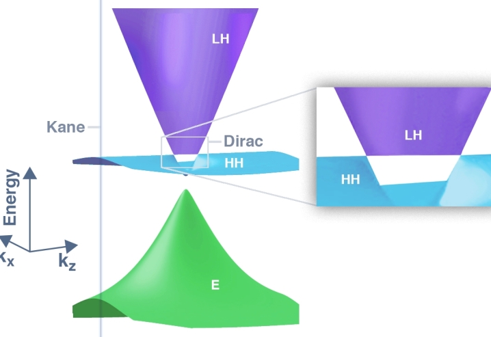
A simplified model of the complex band structure of Cd3As2 has been in the past proposed by Bodnar,Bodnar (1977) who treated this material – in the very first approach – as a conventional narrow-gap Kane semiconductor/semimetalKane (1957) with a nearly vanishing band gap (). The band structure of Cd3As2 thus displays, similar to gapless HgCdTe,Orlita et al. (2014); Teppe et al. (2016) a widely extended conical band, which is centered around the point (Fig. 1). This cone appears due to the approximate accidental degeneracy of - and -like states of arsenic and cadmium, respectively, and is not protected by any symmetry.
A closer look at the band structure of Cd3As2 implied by the model of Bodnar also reveals symmetry-protected Dirac cones. These highly-anisotropic and strongly tilted cones appear – or at least, they are theoretically expected – at low energies, around the crossing points of two arsenic-like -type bands (LH and HH bands in Fig. 1). Such crossing points emerge when the cubic symmetry of a Kane semiconductor/semimetal is reduced to a tetragonal one, which is the case of Cd3As2. The impact of the symmetry lowering on the band structure is quantified by crystal field splitting .Kildal (1974) This parameter describes the energy separation of two -type bands at (degenerate in cubic semiconductorsYu and Cardona (2010)) and directly measures the energy scale of Dirac electrons in Cd3As2.
Reliable experimental estimates of the crystal field splitting and band gap parameters – those which are directly determining the shape and scale of Dirac cones in Cd3As2 – have been missing so far. In this paper, we examine the Cd3As2 bands using Landau level spectroscopy and fill this gap in our understanding of this material. Our results show that cadmium arsenide is a semimetal with a small inverted gap of meV, which may host three-dimensional symmetry-protected Dirac electrons, but only at the energy scale not exceeding several dozens of meV.
II Experimental results and discussion
The experiment was performed on a free-standing 80-m-thick slab of with lateral dimensions of mm2, which was grown in a downstream of the tubular furnace from the polycrystalline phase and later detached from the substrate.Rambo and Aubin (1979) The -ray measurements provided us with a diffraction pattern characteristic of Cd3As2Ali et al. (2014) and also showed the existence of a few monocrystalline grains – all with the (112)-orientation, which is the typical growth direction of this material. Similar to other Cd3As2 crystals, the sample shows -type conductivityRosenman (1969); Zdanowicz et al. (1979); Arushanov (1980, 1992) due to intrinsic defects, with an electron concentration slightly below cm-3.

The studied sample was characterized by zero-field optical spectroscopy in both transmission and reflectivity configurations (Fig. 2a). The reflectivity spectrum, measured using an infrared microscope combined with a conventional Fourier-transform spectrometer, indicates the presence of free charge carriers by a characteristic plasma edge at meV. The fine structure of the plasma edge was also observed in other studies, see, e.g., Refs. Gelten et al., 1980; Neubauer et al., 2016; Akrap et al., 2016; Crassee et al., and it is likely related to non-homogeneous (lateral as well as perpendicular to the surface) distribution of electrons in the explored sample.
The transmission spectrum of the sample shows a well-defined transparency window, which is marked by vertical gray bars in Fig. 2a. At low energies, this transparency window opens just above the plasma edge. At high energies, the transmission window closes due to the onset of interband absorption. The dominant contribution to this absorption arises from electrons excited from the flat (HH) band to the partially occupied upper conical band,Akrap et al. (2016) as schematically shown in the inset of Fig. 2a. The position of the onset of the interband absorption is thus determined by the particular position of the Fermi energy (due to Pauli blocking), which provides us with an estimate of meV. In this estimate we have completely neglected the dispersion of the flat band, which is in reality a hole-like, approximately parabolic band. The corresponding effective mass should be comparable with heavy hole masses in conventional semiconductorsYu and Cardona (2010) (i.e., approaching the mass of a bare electron in vacuum). The dispersion of this band thus may be neglected in the close vicinity of the point – where the studied (magneto-)optical excitations originate – but has to be considered for momenta comparable with the size of the Brillouin zone, which is the typical scale of ARPES experiments.Borisenko et al. (2014); Neupane et al. (2014); Liu et al. (2014)
The onset of interband excitations may be directly seen in the optical conductivity spectrum (Fig. 2b), which was obtained using the standard Kramers-Kronig analysis of the reflectivity response, complemented by ellipsometry data at high photon energies (inset of Fig. 2b). The smooth spectral profile of this onset indicates a certain spread of the Fermi energy across the probed sample, but likely also some defect/impurity-related absorption within the optical band gap. Above the onset of interband excitations, the optical conductivity follows a linear, or more precisely a weakly superlinear, dependence on the photon energy, which is in perfect agreement with previous studies.Neubauer et al. (2016); Akrap et al. (2016) The optical conductivity increasing linearly with the photon frequency, , is typical of systems with 3D massless electrons.Timusk et al. (2013); Orlita et al. (2014) The strong increase in the real part of the optical conductivity at low energies is related to intraband (Drude-type, free-carrier) excitations.
The existence of the well-defined transparency window allowed us to probe the response of the sample in magneto-transmission experiments. To perform such measurements, the radiation of a globar was analysed by a Fourier transform spectrometer and using light-pipe optics, delivered to the sample placed in a superconducting coil. The transmitted light was detected by a composite bolometer, placed directly below the sample and kept at the same temperature as the sample (1.8 K). The measurement was done in the Faraday geometry with light propagating perpendicular to the (112) crystal face.
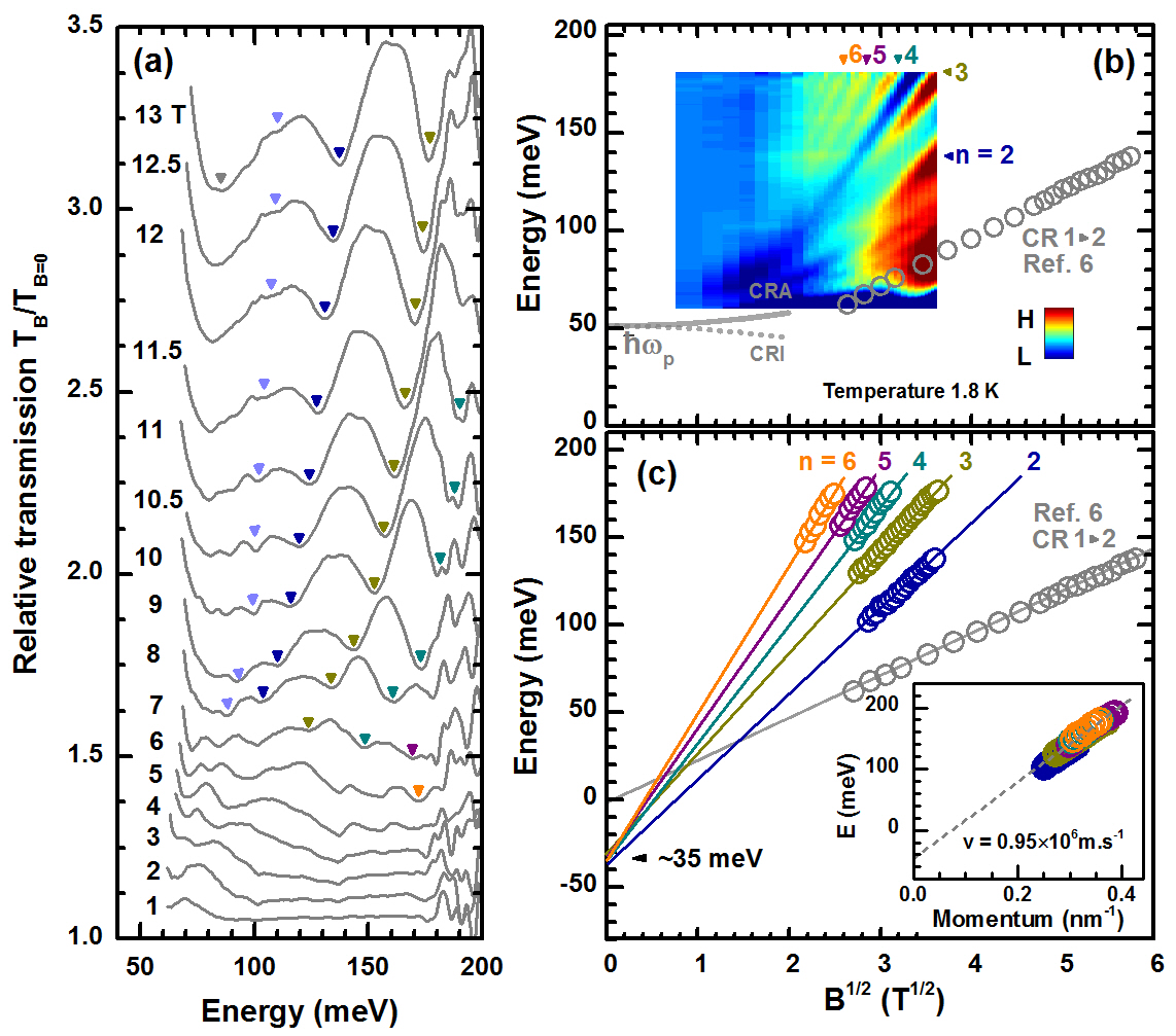
A series of excitations, at energies monotonically increasing with , is clearly seen in the relative magneto-transmission spectra (Fig. 3a) as well as in the false color plot of relative magneto-absorbance (Fig. 3a). These excitations appear in the spectra at photon energies significantly higher than the cyclotron energy in the quantum limit, deduced from our preceding high-field magneto-reflectivity experiment.Akrap et al. (2016) This points towards the interband origin of these inter-Landau level (inter-LL) excitations.
In the limit of low magnetic fields, these interband resonances seem to asymptotically approach the plasma energy (see color plot in Fig. 3b). This behavior may be viewed as an avoided crossing of interband inter-LL excitations with a plasma resonance, known as the Bernstein modes Bernstein (1958). Since the sample is fully opaque at photon frequencies below , we only observe the upper branch of these coupled modes. Such coupling can be clearly visualized in 2D structures with an additional lateral periodic potential. For instance, such modes have been observed in magneto-optics of quantum wellsBatke et al. (1986, 1985) with the use of surface gratings in order to match inter-LL and plasma frequencies. In 3D samples, such as here, this coupling can be observed more easily since the plasma frequency does not vanish at and it was already demonstrated in Raman spectroscopy of -type GaAs.Wysmołek et al. (2006) The magneto-optical effects due to this coupling may be richer in systems with a linear dispersion, the gapless character of which implies a series of interband inter-LL excitations at relatively low energies, as discussed in the context of graphene.Roldán et al. (2011) To compare the energy scales of the avoided crossing related to Bernstein modes with the field-induced splitting of the plasma edge expected within the classical theory of magneto-plasma,Palik and Furdyna (1970) we plotted in Fig. 3b the theoretical positions of the cyclotron resonance active and inactive (CRA and CRI) modes for the corresponding cyclotron mass .
At high photon energies, well above the plasma energy (), the observed transitions correspond to single-particle interband excitations between Landau levels. Tracing their field-dependence may provide us with a useful insight into the electronic band structure of Cd3As2. All excitations show a well-defined dependence, which is in general characteristic of massless charge carriers, nevertheless, with a well defined negative offset of about meV (Fig. 3c). This is in contrast to the cyclotron energy in the quantum limit, which is also linear in , but without any offset.Akrap et al. (2016)
Let us first analyze these data in a simplified way, using the semiclassical Bohr-Sommerfeld quantization,Onsager (1952); Goerbig et al. (2014) which only considers the orbital motion of electrons and neglects their spin. In this picture, the density of states, and consequently, also the joint density of states, becomes modulated due to the quantized cyclotron motion of electrons. With an assumption of isotropic bands (reasonably well justified for Cd3As2 Akrap et al. (2016)) the cyclotron orbits are characterized by the momenta , where is integer () and is a factor related to the Berry phase of the explored charge carriers (). This allows us to reconstruct the original band structure, i.e., to get the energy distance from the valence to conduction band, from which the corresponding LLs are formed (the HH band and the upper cone).
Setting the indices as specified in Fig. 3b,c ( and 6), all experimental points reasonably well fall on a single line (inset of Fig. 3c), thus implying a nearly perfect linear energy-momentum dependence, with the slope reflecting the velocity parameter m/s. In the inset of Fig. 3c, we have considered, consistently with the Kane/Bodnar model, the phase factor . Importantly, the deduced velocity exactly matches the value deduced for the upper conical conduction band in the original analysis of Bodnar,Bodnar (1977) in the more recent STM/STS studyJeon et al. (2014) as well as in cyclotron resonance experiment Akrap et al. (2016). This remarkable agreement may only be explained by the existence of a nearly dispersionless valence band, from which electrons are promoted, via an optical excitation, to the conical conduction band (excitations from the blue to violet band in Fig. 1). This is fully consistent with the Bodnar/Kane modelKane (1957), which implies the existence of such a flat band. On the other hand, no flat band is expected in systems described by the Dirac Hamiltonian.
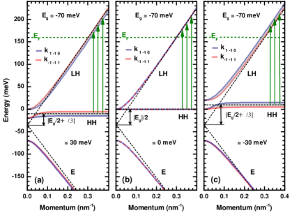
Now we analyze the negative offset of interband inter-LL excitations (seen in Fig. 3) in greater detail. Again, no such offset is expected for Dirac-type systems, with an exception for the unlikely case that the velocity parameter increases isotropically with momentum. This would imply strong parabolic corrections to the linear bands and thus equally strong deviations from the behavior of the magneto-optical transmission lines. The absence of such deviations precludes this type of band corrections as the origin of the negative offset. In contrast, the offset – either positive or negative – is expected in Kane semiconductors/semimetals with a non-zero band gap , as visualized using the asymptotes in Fig. 4b. At photon energies larger than the band gap, , the flat band becomes shifted with respect to the upper cone by , which gives rise to the offset of the interband inter-LL excitations (when followed as a function of ). The same conclusion can be drawn directly from the LL spectrum of Kane electrons. At photon energies significantly higher as compared to , the energies of flat-to-upper-cone inter-LL transitions read (at ): for , where stands for the spin projection, see Ref. Orlita et al., 2014 and related Supplementary materials.
When the full Bodnar model – with a non-zero crystal field splitting parameter – is considered, the situation becomes more complex and the band structure is no longer isotropic. This is best manifested by the modulation of the HH band, which is completely flat only for . This modulation is illustrated in Figs. 4a,c, where the LH, HH and E bands have been plotted for two different crystallographic directions. These are perpendicular to the magnetic field applied along the [112] direction and they were chosen to visualize the full width of the flat band induced by . For relatively small , the HH band remains fairly flat, but it is shifted by the average value of . This implies an approximate offset of flat-to-cone inter-LL excitations: .
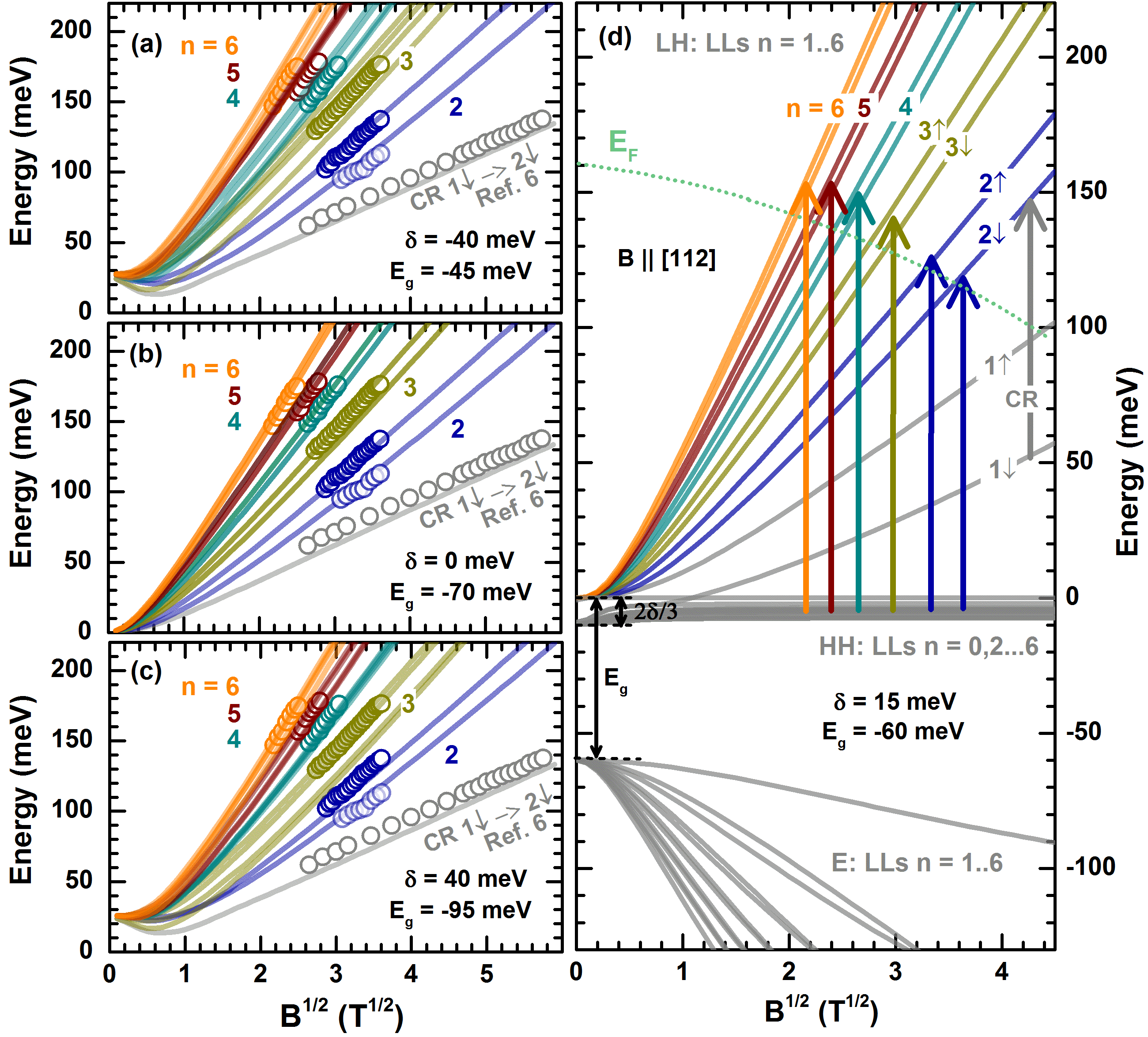
To estimate the and parameters, the simplified analysis of our magneto-optical data based on the semi-classical Bohr-Sommerfeld model (see the inset of Fig. 3c) has to be replaced with full quantum-mechanical treatment. To this end, we have numerically calculated the LL spectrum within the complete Bodnar model for the magnetic field oriented along the [112] direction SM , see Fig. 5. In these calculations, the velocity parameter was considered as isotropic and fixed at m/s, which is a value consistent with the original Bodnar’s analysisBodnar (1977) as well as with more recent STM/STS and cyclotron resonance studies.Jeon et al. (2014); Akrap et al. (2016) The spin-orbit coupling, having rather weak influence on the resulting LL spectrum, was set as meV.Akrap et al. (2016)
The only tunable parameters in the calculations of the LL spectrum in Fig. 5 were thus the band gap and the crystal-field splitting . We have considered their various combinations, with the approximate boundary condition implied by the offset meV determined and discussed above. This is illustrated in Fig. 5, where our calculations are shown for (a): meV, meV, (b) meV, meV and (c) meV, meV, respectively. For electric-dipole-active excitations, which preserve spin and follow the selection rules ,Orlita et al. (2014) we obtain two transitions from the flat band into a given final-state LL with the index or , see Ref. SM, for more details. Experimentally, the splitting of transitions due to spin is resolved only for the lowest final-state LL , cf., Fig. 5d.
The best agreement between the experimental data and theoretically expected energies of inter-LL excitations was found for , for which the Bodnar model reduces down to even more simple Kane model with an effectively vanishing energy scale of Dirac cones. For the crystal-field splitting as low as meV, the departure of theoretical lines from experimental points becomes significant enough that it allows us to set, while being conservative in this estimate, the interval of acceptable values to meV.
Let us recall that it is the sign of the parameter, which determines whether the system with an inverted band gap becomes a 3D Dirac semimetal (for ) or a topological insulator (for ). Clearly, our magneto-optical data do not allow us to determine the sign of . Nevertheless, one may profit, in this case, from ab initio calculations of the Cd3As2 band structure presented, for instance, in Refs. Wang et al., 2013; Ali et al., 2014; Borisenko et al., 2014; Conte et al., 2017. The absolute values of energy splitting and band gaps deduced theoretically may not be very accurate. On the other hand, the ordering of bands, which among other things implies the sign of , represents rather reliable output. The available theoretical works predict positive value of , see, e.g., Refs. Wang et al., 2013; Conte et al., 2017. This allows us to reduce the interval of the expected crystal field splitting to meV.
As a matter of fact, it is the tetragonal lattice of Cd3As2 itself, with the out-of-plane lattice constant elongated with respect to the in-plane components (), which determines the sign of the parameter. In HgTe, which is another well-known Kane semimetal ( meV), lateral expansion of the lattice gives rise to a negative crystal-field splitting (), and therefore, to a topological insulating phase, which has been extensively studied experimentally.Brüne et al. (2011); Dziom et al. (2017) In contrast, compressive lateral strain is expected to transform HgTe into a 3D symmetry-protected Dirac semimetal (with ). Therefore, staying strictly with estimates based on our experimental magneto-optical data ( meV) only, one cannot unambiguously decide whether Cd3As2 is a symmetry-protected Dirac semimetal or a topological insulator with a very narrow band gap in bulk.
Let us also note that the negative sign of the band gap in Cd3As2 reflects an inverted ordering of bands in this system, and consequently, implies the appearance of surface states, similar to those in topological insulators.Hasan and Kane (2010) Such surface states have already been observed in another inverted-gap Kane semimetal HgTe.Liu et al. (2015) In Cd3As2, however, the situation might be more complex. The surface states, which appear due to the band inversion, might coexist with the Fermi arcs, which are predicted for this material due to the presence of a pair of Dirac nodes (two pairs of Weyl nodes) at low energies. At present, our magneto-optical data do not provide us with any clear signature of surface states, but their presence was discussed in the context of ARPES and magneto-transport experiments.Yi et al. (2014); Zhang et al. (2017); Schumann et al. (2018)
III Conclusions
In summary, we have performed magneto-transmission experiments on Cd3As2. The observed magneto-optical response, comprising a series of interband inter-Landau level excitations, allow us to determine the band structure parameters relevant for the scale and shape of possibly present Dirac cones in this material. The estimated crystal field splitting, meV, represents the very upper limit for the energy of Dirac electrons in Cd3As2. These relativistic-like particles thus may emerge in the band structure only at energies far below the Fermi level, which in available samples typically exceeds 100 meV (in our case meV). At energies significantly higher than , the system behaves as an ordinary Kane semimetalKane (1957); Kacman and Zawadzki (1971); Yu and Cardona (2010); Akrap et al. (2016) characterized by a small inverted band gap of meV.
Acknowledgements
This work was supported by ERC MOMB (No. 320590), TWINFUSYON (No. 692034), Lia TeraMIR, TERASENS, by MEYS CEITEC 2020 (No. LQ1601) and by ANR DIRAC3D projects and MoST-CNRS exchange programme (DIRAC3D). We acknowledge the support of LNCMI-CNRS, a member of the European Magnetic Field Laboratory (EMFL). The authors also acknowledge discussions with D. M. Basko, A. O. Slobodeniuk and N. Miller. A. A. acknowledges funding from The Ambizione Fellowship of the Swiss National Science Foundation. I. C. acknowledges support from the postdoc mobility programme of the Swiss NSF.
References
- Wang et al. (2013) Z. Wang, H. Weng, Q. Wu, X. Dai, and Z. Fang, Phys. Rev. B 88, 125427 (2013).
- Borisenko et al. (2014) S. Borisenko, Q. Gibson, D. Evtushinsky, V. Zabolotnyy, B. Büchner, and R. J. Cava, Phys. Rev. Lett. 113, 027603 (2014).
- Neupane et al. (2014) M. Neupane, S.-Y. Xu, R. Sankar, N. Alidoust, G. Bian, C. Liu, I. Belopolski, T.-R. Chang, H.-T. Jeng, H. Lin, et al., Nature Comm. 5, 3786 (2014).
- Liu et al. (2014) Z. K. Liu, B. Zhou, Y. Zhang, Z. J. Wang, H. M. Weng, D. Prabhakaran, S.-K. Mo, Z. X. Shen, Z. Fang, X. Dai, Z. Hussain, and Y. L. Chen, Science 343, 864 (2014).
- Jeon et al. (2014) S. Jeon, B. B. Zhou, A. Gyenis, B. E. Feldman, I. Kimchi, A. C. Potter, Q. D. Gibson, R. J. Cava, A. Vishwanath, and A. Yazdani, Nature Mater. 13, 851 (2014).
- Akrap et al. (2016) A. Akrap, M. Hakl, S. Tchoumakov, I. Crassee, J. Kuba, M. O. Goerbig, C. C. Homes, and et al., Phys. Rev. Lett. 117, 136401 (2016).
- Conte et al. (2017) A. M. Conte, O. Pulci, and F. Bechstedt, Sci. Rep. 7, 45500 (2017).
- Bodnar (1977) J. Bodnar, in Proc. III Conf. Narrow-Gap Semiconductors, Warsaw, edited by J. Raułuszkiewicz, M. Górska, and E. Kaczmarek (Elsevier, 1977) p. 311.
- Kane (1957) E. O. Kane, J. Phys. Chem. Solids 1, 249 (1957).
- Orlita et al. (2014) M. Orlita, D. M. Basko, M. S. Zholudev, F. Teppe, W. Knap, V. I. Gavrilenko, N. N. Mikhailov, S. A. Dvoretskii, P. Neugebauer, C. Faugeras, et al., Nature Phys. 10, 233 (2014).
- Teppe et al. (2016) F. Teppe, M. Marcinkiewicz, S. S. Krishtopenko, S. Ruffenach, C. Consejo, A. M. Kadykov, W. Desrat, D. But, W. Knap, J. Ludwig, S. Moon, D. Smirnov, M. Orlita, Z. Jiang, S. V. Morozov, V. I. Gavrilenko, N. N. Mikhailov, and S. A. Dvoretskii, Nature Commun. 7, 12576 (2016).
- Kildal (1974) H. Kildal, Phys. Rev. B 10, 5082 (1974).
- Yu and Cardona (2010) P. Y. Yu and M. Cardona, Fundamentals of Semiconductors (Springer, Berlin Heidelberg, 2010).
- Rambo and Aubin (1979) A. Rambo and M. J. Aubin, Can. J. Phy. 57, 2093 (1979).
- Ali et al. (2014) M. N. Ali, Q. Gibson, S. Jeon, B. B. Zhou, A. Yazdani, and R. J. Cava, Inorganic Chemistry 53, 4062 (2014).
- Rosenman (1969) I. Rosenman, J. Phys. Chem. Solids 30, 1385 (1969).
- Zdanowicz et al. (1979) W. Zdanowicz, L. Zdanowicz, J. Portal, and S. Askenazy, Thin Solid Films 61, 41 (1979).
- Arushanov (1980) E. Arushanov, Prog. Cryst. Growth Ch. 3, 211 (1980).
- Arushanov (1992) E. Arushanov, Prog. Cryst. Growth Ch. 25, 131 (1992).
- Gelten et al. (1980) M. Gelten, C. van Es, F. Blom, and J. Jongeneelen, Solid State Commun. 33, 833 (1980).
- Neubauer et al. (2016) D. Neubauer et al., Phys. Rev. B 93, 121202 (2016).
- (22) I. Crassee, E. Martino, C. C. Homes, O. Caha, J. Novak, P. Tuckmantel, M. Hakl, A. Nateprov, E. Arushanov, Q. Gibbson, R. Cava, S. Koohpayeh, K. Arpino, T. McQueen, M. Orlita, and A. Akrap, arxiv:1712.03147 .
- Timusk et al. (2013) T. Timusk, J. P. Carbotte, C. C. Homes, D. N. Basov, and S. G. Sharapov, Phys. Rev. B 87, 235121 (2013).
- Bernstein (1958) I. B. Bernstein, Phys. Rev. 109, 10 (1958).
- Batke et al. (1986) E. Batke, D. Heitmann, and C. W. Tu, Phys. Rev. B 34, 6951 (1986).
- Batke et al. (1985) E. Batke, D. Heitmann, J. P. Kotthaus, and K. Ploog, Phys. Rev. Lett. 54, 2367 (1985).
- Wysmołek et al. (2006) A. Wysmołek, D. Plantier, M. Potemski, T. Słupiński, and Z. R. Żytkiewicz, Phys. Rev. B 74, 165206 (2006).
- Roldán et al. (2011) R. Roldán, M. O. Goerbig, and J.-N. Fuchs, Phys. Rev. B 83, 205406 (2011).
- Palik and Furdyna (1970) E. D. Palik and J. Furdyna, Rep. Prog. Phys. 33, 1193 (1970).
- Onsager (1952) L. Onsager, Philos. Mag. 43, 1006 (1952).
- Goerbig et al. (2014) M. O. Goerbig, G. Montambaux, and F. Pi chon, EPL (Europhysics Letters) 105, 57005 (2014).
- (32) See Supplementary materials, which include Refs. 33 and 34, for details about theoretical model and data analysis.
- Wallace (1979) P. R. Wallace, phys. stat. sol. (b) 92, 49 (1979).
- Orlita et al. (2012) M. Orlita, P. Neugebauer, C. Faugeras, A.-L. Barra, M. Potemski, F. M. D. Pellegrino, and D. M. Basko, Phys. Rev. Lett. 108, 017602 (2012).
- Brüne et al. (2011) C. Brüne, C. X. Liu, E. G. Novik, E. M. Hankiewicz, H. Buhmann, Y. L. Chen, X. L. Qi, Z. X. Shen, S. C. Zhang, and L. W. Molenkamp, Phys. Rev. Lett. 106, 126803 (2011).
- Dziom et al. (2017) V. Dziom, A. Shuvaev, A. Pimenov, G. V. Astakhov, C. Ames, K. Bendias, J. Böttcher, G. Tkachov, E. M. Hankiewicz, C. Brüne, et al., Nature Commun. 8, 15197 (2017).
- Hasan and Kane (2010) M. Z. Hasan and C. L. Kane, Rev. Mod. Phys. 82, 3045 (2010).
- Liu et al. (2015) C. Liu, G. Bian, T.-R. Chang, K. Wang, S.-Y. Xu, I. Belopolski, I. Miotkowski, H. Cao, K. Miyamoto, C. Xu, C. E. Matt, T. Schmitt, N. Alidoust, M. Neupane, H.-T. Jeng, H. Lin, A. Bansil, V. N. Strocov, M. Bissen, A. V. Fedorov, X. Xiao, T. Okuda, Y. P. Chen, and M. Z. Hasan, Phys. Rev. B 92, 115436 (2015).
- Yi et al. (2014) H. Yi, Z. Wang, C. Chen, Y. Shi, Y. Feng, A. Liang, Z. Xie, S. He, J. He, Y. Peng, X. Liu, Y. Liu, L. Zhao, G. Liu, X. Dong, J. Zhang, M. Nakatake, M. Arita, K. Shimada, H. Namatame, M. Taniguchi, Z. Xu, C. Chen, X. Dai, Z. Fang, and X. J. Zhou, Sci. Rep. 4 (2014), 10.1038/srep06106.
- Zhang et al. (2017) C. Zhang, A. Narayan, S. Lu, J. Zhang, H. Zhang, Z. Ni, X. Yuan, Y. Liu, J.-H. Park, E. Zhang, et al., Nature Communications 8, 1272 (2017).
- Schumann et al. (2018) T. Schumann, L. Galletti, D. A. Kealhofer, H. Kim, M. Goyal, and S. Stemmer, Phys. Rev. Lett. 120, 016801 (2018).
- Kacman and Zawadzki (1971) P. Kacman and W. Zawadzki, phys. stat. sol. (b) 47, 629 (1971).
![[Uncaptioned image]](/html/1803.05469/assets/x3.png)
![[Uncaptioned image]](/html/1803.05469/assets/x4.png)
![[Uncaptioned image]](/html/1803.05469/assets/x5.png)
![[Uncaptioned image]](/html/1803.05469/assets/x6.png)
![[Uncaptioned image]](/html/1803.05469/assets/x7.png)