Efficient first principles simulation of electron scattering factors for transmission electron microscopy
Abstract
Electron microscopy is a powerful tool for studying the properties of materials down to their atomic structure. In many cases, the quantitative interpretation of images requires simulations based on atomistic structure models. These typically use the independent atom approximation that neglects bonding effects, which may, however, be measurable and of physical interest. Since all electrons and the nuclear cores contribute to the scattering potential, simulations that go beyond this approximation have relied on computationally highly demanding all-electron calculations. Here, we describe a new method to generate ab initio electrostatic potentials when describing the core electrons by projector functions. Combined with an interface to quantitative image simulations, this implementation enables an easy and fast means to model electron microscopy images. We compare simulated transmission electron microscopy images and diffraction patterns to experimental data, showing an accuracy equivalent to earlier all-electron calculations at a much lower computational cost.
keywords:
TEM , QSTEM , DFT , 2D materials1 Introduction
Recent decades have seen enormous advances in electron microscopy instrumentation, steadily increasing its power as a central tool for materials science [1, 2, 3, 4, 5, 6, 7, 8]. Accurate modelling of electron scattering from solids can be crucial for the interpretation of images and electron diffraction data, and hence, key to obtaining insights to the studied materials. In electron diffraction and phase contrast imaging modes such as electron ptychography and high resolution transmission electron microscopy (HRTEM) the observed contrast is dominated by the phase shifts accumulated by the fast electrons that traverse the sample. These shifts can be derived from the electrostatic potential within the sample[9, 10].
Different approximations for the sample potential exist. In the simplest approximation, a screened Coulomb (SC) potential can be used [11, 12, 13], which has the advantage that the electron scattering factor can be expressed in a simple analytic form. However it neglects any details of the atomic electrons’ arrangement into specific orbitals. The independent atom model (IAM) approximates the sample as a superposition of electrostatic potentials previously calculated by first principles for an isolated atom of every element, with several different numerical parameterizations available in the literature [14, 15, 16, 17, 18]. Naturally, this approximation neglects any changes in the electronic charge density that results from interatomic interactions.
For periodic structures, electron and x-ray diffraction patterns are sensitive to the charge transfer in chemical bonds [19, 20, 21, 22]. The analysis of such measurements requires a description beyond the IAM, and can provide insights not only into the atomic configuration but also into the electronic structure of a material. The difference between the IAM and a first principles simulation is in many cases large enough to be directly detectable in HRTEM images [23, 24], and can be crucial for the interpretation of small differences in the atomic contrast [25]. The need for a first-principles based simulation for interpreting the small contrast differences between boron, carbon and nitrogen in experimental HRTEM data was demonstrated earlier by some of the authors of the current work [26].
Nearly all previous works have utilized computationally expensive all-electron density functional theory (DFT) [27, 28, 23], apart from a recent effort to extract the electrostatic potential from a pseudopotential calculation [29]. However, since that method does not explicitly give the core electron charge needed for TEM simulations, the authors had to resort to a correction scheme [30]. By contrast, the projector-augmented waves we use here allow the exact (frozen) core electron density to be recovered. Our approach is thus a simple and accurate way to calculate the electrostatic potential in the sample and the subsequent electron scattering factors.
For TEM image simulation, we compare the results of our method to previous experiments and to all-electron DFT based simulations. In addition, by comparing multiple multiple IAM parameterizations, we show that experimental electron diffraction patterns of graphene and hexagonal boron nitride (hBN) can be simulated with a near-perfect match only when bonding effects are taken into account.
2 Methods
2.1 Theory
In the projector-augmented wave (PAW) formalism [31], the total charge density is a sum of the squared all-electron valence wave functions, the frozen core electron density, and the nuclear charges. For practical calculations, the charge density is divided into a smooth part plus corrections for each atom : , where the smooth part is given in terms of pseudo wave functions and pseudo core charges. By construction, the multipole moments of are zero and therefore the electrostatic potential from these correction charges will be non-zero only inside the atomic augmentation spheres.
This allows us to solve the Poisson equation in two separated steps to obtain the electrostatic potential . First for the “pseudo” part,
| (1) |
solved for in all of space on a uniform 3D grid. As second step, the corrections to are added, via
| (2) |
which is solved for on a fine radial grid inside the atomic spheres, here only taking the spherical part of the density into account.
As a final approximation, we broaden the nuclear charges by Gaussian functions (width 0.005 Å) in the total charge density to avoid the corrections diverging as near the nuclei. A detailed description is given in Appendix A.
2.2 Simulation
To simulate electron microscopy images and diffraction patterns, we use the recently implemented PyQSTEM interface to the Quantitative TEM/STEM Simulations (QSTEM) code [32]. Electron scattering is modelled by dividing the simulation cell into slices in the direction perpendicular to the direction of the electron beam, and calculating the propagation of the electron waves from the projected electrostatic potential in each slice to the next. A description of the multislice propagation method can be found in Ref. [32]. In the case of the IAM model, a potential is numerically generated based on the positions and atomic species of the modelled material, with parameterizations of Weickenmeier [15], Peng [16], Kirkland [17] and Lobato [18] available in PyQSTEM in addition to the default QSTEM choice of Rez et al. [33]. In the ab initio approach, the potential is instead derived from the ground state electron and nuclear charge density obtained from DFT (or another first principles simulation method). In the present work, we use the PAW-based code GPAW [34, 35], which we compare to earlier Wien2k calculations. [25] Finally, to most directly assess the role of chemical bonding, we parameterized an additional IAM potential based on isolated-atom GPAW calculations.
2.2.1 PyQSTEM
PyQSTEM is a Python based interface and extension to the multislice simulation program QSTEM. It was created with the goal of providing a single scripting environment for doing everything related to image simulation, from model building to analysis. This allows simulating large numbers of automatically generated models required for purposes such as statistical analysis, optimization and machine learning. PyQSTEM provides a large degree of flexibility by letting the user supply any custom wave function or potential, and is especially convenient with GPAW.
Python is a well suited interface language due to its prevalence in data science. The numerous extension packages such as numpy [36] and scipy [37] provide direct access to tools for image analysis. The Atomic Simulation Environment (ASE) [38] is used for building atomic models. This is a popular tool in the computational materials community, with modules for defining a wide range of different structures. By using ASE it is easy to integrate results from atomistic simulations into microscopy simulations. The PyQSTEM program and all its dependencies are open source under the GNU general public license [39], and available on all platforms [40].
2.2.2 TEM simulation with DFT potential
To simulate TEM images and electron diffraction patterns, we start by building orthorhombic unit cells on the -plane using ASE, as PyQSTEM assumes propagation along the -direction. We assign a GPAW calculator created in the finite difference (FD) mode where the wave functions are represented on a real space grid.
We then run a DFT calculation with the PBE functional. When this is finished, we can extract the all-electron potential, using the method described in Section 2.1 dubbed PS2AE (PSeudo wave to All-Electron wave). The resulting numpy array, v, describes the all-electron potential on a 3D grid in ASE units (eV). The multislice algorithm requires slices of this potential projected along the beam direction
| (3) |
where is the slice and is the slice thickness. By also supplying the unit cell, we fix the lateral sampling rate of the TEM simulation.
We then use PyQSTEM in TEM mode; other modes currently supported are STEM and convergent-beam electron diffraction. We set the potential and build a plane wave function at an acceleration voltage of 80 kV. Finally, we run a multislice simulation, propagating the wave function through the potential once.
We can also directly obtain the electron diffraction pattern, which is very useful for quantitative comparison to experiment, as the absolute square of the Fourier transform of the exit wave (a logarithm is easier to visualize, but less useful for the quantification of diffraction intensities). The code that we use is provided in the Supplemental Materials.
2.3 Experiment
To compare the simulations with HRTEM images, we refer to published work on hexagonal boron nitride (hBN) [26]. To further quantify the accuracy, we compare our simulations to electron diffraction measurements of mechanically exfoliated single-layer graphene and single-layer hBN synthesized by chemical vapor deposition [41, 42]. The diffraction patterns were recorded on an aberration-corrected FEI Titan 80-300 and on a Philips CM200 microscope (both operated at 80 kV).
3 Results and discussion
3.1 Benchmarking
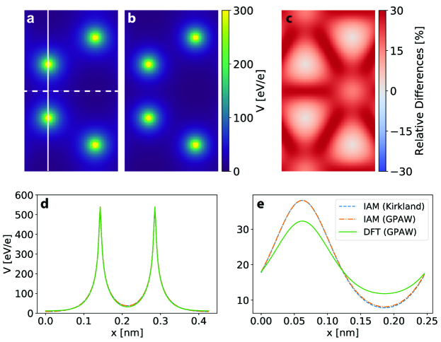
In Fig. 1 we show the potential of graphene calculated using the Kirkland IAM, our GPAW-based IAM, and via first principles with GPAW as specified above. Since the latter two are based on the same method for calculating the electrostatic potential but one includes chemical bonding, this serves as a direct comparison of its influence. It may seem counter-intuitive that the IAM potential is greater along the C-C bonds (Fig. 1). However, this is because the main effect of the electron density is to screen the Coulomb potential of the cores [43]. Consequently, bonding concentrates the electron density into the near core regions and between the atoms, reducing the total potential in these regions.
We further studied how the DFT parameters affect the integrated electrostatic potential of the four-atom orthogonal unit cell of graphene, calculated using the PBE functional [44] (Fig. 2; LDA yields 0.5% higher values). For this measure, we find full convergence with an electrostatic grid spacing111The electrostatic grid spacing sets the real-space density of the arrays used to describe the electrostatic potential and is important for solving the Poisson equation accurately. of 0.02 Å and a nuclear charge broadening of 0.005 Å, a computational grid spacing222Defines the real-space density of the arrays to describe the electron density numerically, fulfilling a similar convergence role as a plane wave cutoff energy, but is not strictly variational. of 0.16 Å (the default 0.2 Å is practically converged), a -point mesh finer than 7131, and a Poisson solver convergence criterion333This criterion is similar to convergence criteria for wave functions and electron density, but instead for solving the Poisson equation within each step of the self-consistency cycle. of 10-12, slightly tighter than the default. For graphene, at least 10 Å of vacuum is required. In the following, we use fully converged parameters.

3.1.1 Comparison to Wien2k
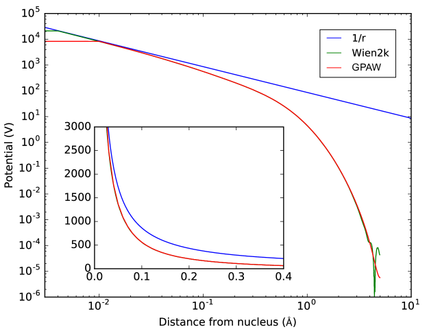
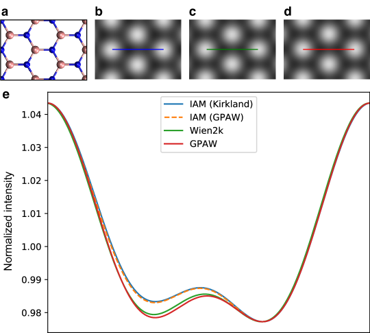
It is of interest to compare our results to an established all-electron method, such as the Wien2k code (as described in Ref. 25). For the potential near a C nucleus, apart from the slightly different low-distance cutoff (determined by the electrostatic grid spacing, here 0.01 Å) and minor numerical variation at the periodic cell boundary, the results are identical (Fig. 3). In Fig. 4 we further compare HRTEM simulations of hBN as reported experimentally and using Wien2k in Ref. 26. Due to a neglect of bonding effects, the IAM predicts a significant asymmetry in the image contrast over the B and N sites. However, an image simulated using the full electrostatic potential derived here correctly predicts a much lesser asymmetry, in a excellent agreement with previous results from Wien2k and with the experiment shown in Ref. 26.
Despite this identical accuracy, our method is significantly faster. Using our converged parameters, a full calculation from a relaxed hBN structure to its electrostatic potential takes only 6 min, compared to 142 min for Wien2k running on the same hardware. An image simulation depends on the number of slices, and only takes some minutes. Furthermore, GPAW scales efficiently to far more cores and larger systems.
3.1.2 Electron diffraction
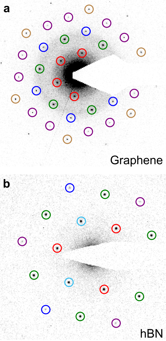
The graphene diffraction pattern (Fig. 5a) exhibits the six-fold symmetry of the lattice. We compare the relative intensities of the first and second set of diffraction peaks, averaging over equivalent peaks and using the innermost ring as reference (intensity = 1). It is important to emphasize that we measure the integrated intensity of each diffraction peak (minus surrounding background) rather than the peak intensity of a line profile, which would be affected by peak broadening.
In high-quality graphene, the ratio of the second- to first-order peaks is very close to 1.0, sometimes even slightly higher (in the pattern in Fig. 5, the ratio is 1.04). Highly defective graphene (e.g. graphene oxide), by contrast, shows a much lower ratio [45, 46], which can be attributed to a static Debye-Waller factor (DWF) resulting from a structure with imperfect periodicity. The IAM predicts a ratio of 0.89, while the first-principles calculation predicts a ratio of 1.10. Considering that any DWF (static from disorder, or dynamic from atomic motion) can only reduce the ratio, the IAM is in clear conflict with our experimental values. However, for the first principles calculation, including the DWF as measured in Ref. 13 results in an excellent agreement with experiment.
The single-layer hBN diffraction pattern (Fig. 5b) exhibits the expected three-fold symmetry in the innermost ring, a six-fold symmetry in the second ring, and again three-fold symmetry in the third ring (hexagonal symmetry with two inequivalent atoms). We use the weaker inner spot as reference (intensity = 1) and measure (Fig. 5) the intensities of the other peaks. Our first principles calculation is in near-perfect agreement for the experimental first, third and fourth intensity ratios, but diverges slightly for the second one (1.16 vs. 1.07). However, including the DWFs again brings the simulated intensity into excellent agreement with experiment.
Tables 1 and 2 lists the experimental and simulated diffraction peak intensities. We use DWFs for graphene and for hBN from Ref. 13, given as ratios of the DWF with respect to the reference peak. The lower parts of the tables show the simulated diffraction intensities multiplied with this DWF ratio, which is the set of values that should be compared to the experiment. Multiplying the simulated ratios with the DFWs brings the sum of errors in the first four ratios to within 1% of experiment for graphene and 2% for hBN. This remarkably good agreement can only be achieved with a DFT electrostatic potential.
| Graphene | ||||
|---|---|---|---|---|
| Experiment | 1.03 | 0.16 | 0.05 | 0.12 |
| Wien2k | 1.10 | 0.18 | 0.06 | 0.15 |
| GPAW | 1.11 | 0.18 | 0.06 | 0.15 |
| IAM (GPAW) | 0.99 | 0.16 | 0.07 | 0.18 |
| IAM (Kirkland) | 0.98 | 0.16 | 0.06 | 0.17 |
| IAM (Lobato) | 0.98 | 0.16 | 0.06 | 0.17 |
| IAM (Weickenmeier) | 0.93 | 0.15 | 0.07 | 0.18 |
| IAM (Peng) | 0.92 | 0.14 | 0.06 | 0.14 |
| IAM (Rez) | 0.89 | 0.14 | 0.05 | 0.12 |
| DWF ratio | 0.93 | 0.89 | 0.79 | 0.74 |
| Wien2kDWF | 1.02 | 0.14 | 0.05 | 0.11 |
| GPAWDWF | 1.03 | 0.14 | 0.05 | 0.11 |
| IAM (Kirkland)DWF | 0.91 | 0.14 | 0.05 | 0.13 |
| hBN | ||||
|---|---|---|---|---|
| Experiment | 1.05 | 1.07 | 0.19 | 0.19 |
| Wien2k | 1.05 | 1.17 | 0.16 | 0.17 |
| GPAW | 1.06 | 1.16 | 0.16 | 0.17 |
| IAM (GPAW) | 1.07 | 0.95 | 0.17 | 0.16 |
| IAM (Kirkland) | 1.07 | 0.96 | 0.17 | 0.16 |
| IAM (Lobato) | 1.07 | 0.96 | 0.17 | 0.16 |
| IAM (Peng) | 1.06 | 0.94 | 0.16 | 0.16 |
| IAM (Weickenmeier) | 1.07 | 0.94 | 0.17 | 0.16 |
| IAM (Rez) | 1.07 | 0.95 | 0.13 | 0.13 |
| DWF ratio | 1 | 0.93 | 0.89 | 0.89 |
| Wien2kDWF | 1.05 | 1.09 | 0.15 | 0.16 |
| GPAWDWF | 1.06 | 1.08 | 0.15 | 0.16 |
| IAM (Kirkland)DWF | 1.07 | 0.89 | 0.15 | 0.14 |
4 Conclusions
Efficient simulation of the full electrostatic potential of materials is becoming ever more important with the development of better instrumentation. Approximate models, though feasible for large systems and sufficient for routine simulations, do not capture bonding effects that can in some cases be directly measured, nor are they sufficient for electron holography. We have shown how the electrostatic potential derived from frozen core projector-augmented wave density functional theory gives a description of electron scattering equal to previously available and significantly more demanding methods such as Wien2k, and in excellent agreement with experiment on graphene and hexagonal boron nitride.
Due to its computational efficiency, our approach opens the way for the treatment of large systems with defects, such as impurities or grain boundaries, and is not limited to two-dimensional specimens. Although we have chosen to concentrate on high-resolution transmission electron microscopy due to its greater sensitivity to bonding effects, scanning TEM images can equally well be simulated. The current implementation provides a convenient computational workflow starting from a structure model all the way to high-quality images or diffraction patterns in one simple script.
Acknowledgments
We thank Bernhard C. Bayer for providing the experimental hBN diffraction pattern. T.S. acknowledges the Austrian Science Fund (FWF) for funding via project P 28322-N36, J.C.M. via project P25721-N20, and J.K. via project I 3181-N36. U.L. and J.K were supported by the Wiener Wissenschafts-, Forschungs- und Technologiefonds (WWTF) via project MA14-009. T.J.P acknowledges funding from European Union’s Horizon 2020 Research and Innovation Programme under the Marie Skłodowska-Curie grant agreement no. 655760–DIGIPHASE. Z.L. and U.K. acknowledge funding from the German Research Foundation (DFG) and the Ministry of Science, Research and the Arts (MWK) of Baden-Württemberg in the frame of the Sub-Ångstrom Low-Voltage Electron microscopy (SALVE) project. J.M. acknowledges funding through grant 1335-00027B from the Danish Council for Independent Research.
Appendix A Electrostatic potential
In the projector-augmented wave (PAW) formalism [31], the total charge density (for convenience, we count electrons as positive and protons as negative charge) can be written as
| (4) |
where are the all-electron valence wave functions explicitly included in the calculation ( is the band index and is the crystal momentum) and are occupation numbers. For atom number , is the frozen core electron density, is the position and is the atomic number. For practical calculations, the charge density is divided into a smooth part plus corrections for each atom:
| (5) |
where the smooth part is given in terms of pseudo wave functions , pseudo core charges , expansion coefficients (to be defined below) and localized shape functions that in the GPAW code[34, 35] have been chosen to be Gaussian functions :
| (6) |
where and are the azimuthal and magnetic quantum numbers, are the spherical harmonics, and the atom-dependent decay factor is chosen such that the charges are localized within the augmentation sphere.
The corrections look similar to the definitions of and except that we now expand the wave functions in all-electron and pseudo partial waves and :
| (7) |
| (8) |
The atomic density matrix is evaluated from projections of the pseudo wave functions onto smooth PAW projector functions localized inside the each atomic augmentation sphere:
| (9) |
The coefficients are chosen so that all multipole moments of are zero and therefore the electrostatic potential from these correction charges will be non-zero only inside the atomic augmentation spheres.
This allows us to solve the Poisson equation in two separated steps, first for the pseudo part:
| (10) |
solved for in all of space on a uniform 3D grid.
In the second step, corrections are added to :
| (11) |
solved for on a fine radial grid inside the atomic spheres only taking the spherical part of the density into account. As a final approximation, we replace in eq. (7) by (with Å) to avoid the corrections diverging as near the nuclei.
References
- [1] M. Haider, S. Uhlemann, E. Schwan, H. Rose, B. Kabius, K. Urban, Electron microscopy image enhanced, Nature 392 (6678) (1998) 768–769.
- [2] O. Krivanek, Towards sub-Å electron beams, Ultramicroscopy 78 (1999) 1–11. doi:10.1016/S0304-3991(99)00013-3.
- [3] F. Haguenau, P. W. Hawkes, J. L. Hutchison, B. Satiat-Jeunemaître, G. T. Simon, D. B. Williams, Key events in the history of electron microscopy., Microscopy and microanalysis : the official journal of Microscopy Society of America, Microbeam Analysis Society, Microscopical Society of Canada 9 (2) (2003) 96–138. doi:10.1017/S1431927603030113.
- [4] P. D. Nellist, M. F. Chisholm, N. Dellby, O. L. Krivanek, M. F. Murfitt, Z. S. Szilagyi, A. R. Lupini, A. Borisevich, W. H. Sides, S. J. Pennycook, Direct sub-Angstrom imaging of a crystal lattice, Science 305 (5691) (2004) 1741. doi:10.1126/science.1100965.
- [5] P. W. Hawkes, Aberration correction past and present, Philosophical Transactions of the Royal Society of London A: Mathematical, Physical and Engineering Sciences 367 (1903) (2009) 3637–3664. doi:10.1098/rsta.2009.0004.
- [6] O. L. Krivanek, G. J. Corbin, N. Dellby, B. F. Elston, R. J. Keyse, M. F. Murfitt, C. S. Own, Z. S. Szilagyi, J. W. Woodruff, An electron microscope for the aberration-corrected era, Ultramicroscopy 108 (3) (2008) 179–195. doi:10.1016/j.ultramic.2007.07.010.
- [7] K. W. Urban, Is science prepared for atomic-resolution electron microscopy?, Nature Materials 8 (4) (2009) 260–2. doi:10.1038/nmat2407.
- [8] R. Erni, Aberration-corrected Imaging in Transmission Electron Microscopy: An Introduction, World Scientific, 2010.
- [9] P. Buseck, J. M. Cowley, L. Eyring, High-resolution transmission electron microscopy and associated techniques, Oxford University Press, 1992.
- [10] J. C. H. Spence, High-Resolution Electron Microscopy, Oxford University Press, 2009.
- [11] G. Wentzel, Zwei Bemerkungen ueber die Zerstreuung korpuskularer Strahlen als Beugungserscheinung, Zeitschrift fuer Physik 40 (8) (1926) 590–593. doi:10.1007/BF01390457.
- [12] M. Rühle, F. F. Ernst, High-resolution imaging and spectrometry of materials, Springer, 2003.
- [13] B. Shevitski, M. Mecklenburg, W. A. Hubbard, E. R. White, B. Dawson, M. S. Lodge, M. Ishigami, B. C. Regan, Dark-field transmission electron microscopy and the Debye-Waller factor of graphene, Physical Review B - Condensed Matter and Materials Physics 87 (4) (2013) 045417. doi:10.1103/PhysRevB.87.045417.
- [14] P. A. Doyle, P. S. Turner, Relativistic Hartree–Fock X-ray and electron scattering factors, Acta Crystallographica Section A 24 (3) (1968) 390–397. doi:10.1107/S0567739468000756.
- [15] A. Weickenmeier, H. Kohl, Computation of absorptive form factors for high-energy electron diffraction, Acta Crystallographica Section A 47 (5) (1991) 590–597. arXiv:https://onlinelibrary.wiley.com/doi/pdf/10.1107/S0108767391004804, doi:10.1107/S0108767391004804.
- [16] L.-M. Peng, G. Ren, S. L. Dudarev, M. J. Whelan, Robust parameterization of elastic and absorptive electron atomic scattering factors, Acta Crystallographica Section A 52 (2) (1996) 257–276. arXiv:https://onlinelibrary.wiley.com/doi/pdf/10.1107/S0108767395014371, doi:10.1107/S0108767395014371.
- [17] E. J. Kirkland, Advanced Computing in Electron Microscopy, Plenum, 1998.
- [18] I. Lobato, D. Van Dyck, An accurate parameterization for scattering factors, electron densities and electrostatic potentials for neutral atoms that obey all physical constraints, Acta Crystallographica Section A 70 (6) (2014) 636–649. doi:10.1107/S205327331401643X.
- [19] T. S. Koritsanszky, P. Coppens, Chemical applications of X-ray charge-density analysis, Chemical Reviews 101 (6) (2001) 1583–627. doi:10.1021/cr990112c.
- [20] L. Wu, Y. Zhu, J. Tafto, Test of first-principle calculations of charge transfer and electron-hole distribution in oxide superconductors by precise measurements of structure factors, Physical Review B 59 (9) (1999) 6035–6038. doi:10.1103/PhysRevB.59.6035.
- [21] S. Shibata, Molecular electron density from electron scattering, Journal of Molecular Structure 485-486 (1-3) (1999) 1–11. doi:10.1016/S0022-2860(99)00178-7.
- [22] J. M. Zuo, M. Kim, J. C. H. Spence, Direct observation of d-orbital holes and Cu ± Cu bonding in Cu 2 O, Nature 401 (6748) (1999) 49–52. doi:10.1038/43403.
- [23] B. Deng, L. D. Marks, Theoretical structure factors for selected oxides and their effects in high-resolution electron-microscope (HREM) images., Acta crystallographica. Section A, Foundations of crystallography 62 (Pt 3) (2006) 208–16. doi:10.1107/S010876730601004X.
- [24] B. Deng, L. D. Marks, J. M. Rondinelli, Charge defects glowing in the dark., Ultramicroscopy 107 (4-5) (2007) 374–81. doi:10.1016/j.ultramic.2006.10.001.
- [25] S. Kurasch, J. C. Meyer, D. Künzel, A. Groß, U. Kaiser, Simulation of bonding effects in hrtem images of light element materials, Beilstein Journal of Nanotechnology 2 (2011) 394–404. doi:10.3762/bjnano.2.45.
- [26] J. C. Meyer, S. Kurasch, H. J. Park, V. Skakalova, D. Künzel, A. Groß, A. Chuvilin, G. Algara-Siller, S. Roth, T. Iwasaki, U. Starke, J. H. Smet, U. Kaiser, Experimental analysis of charge redistribution due to chemical bonding by high-resolution transmission electron microscopy, Nat. Mater. 10 (3) (2011) 209–215. doi:10.1038/nmat2941.
- [27] T. Gemming, G. Möbus, M. Exner, Ernst, M. Rühle, Ab-initio HRTEM simulations of ionic crystals: a case study of sapphire, Journal of Microscopy 190 (1–2) (1998) 89–98. doi:10.1046/j.1365-2818.1998.3110863.x.
- [28] S. Mogck, B. Kooi, J. De Hosson, M. Finnis, Ab initio transmission electron microscopy image simulations of coherent Ag-MgO interfaces, Physical Review B 70 (24) (2004) 1–9. doi:10.1103/PhysRevB.70.245427.
- [29] S. Borghardt, F. Winkler, Z. Zanolli, M. J. Verstraete, J. Barthel, A. H. Tavabi, R. E. Dunin-Borkowski, B. E. Kardynal, Quantitative agreement between electron-optical phase images of and simulations based on electrostatic potentials that include bonding effects, Phys. Rev. Lett. 118 (2017) 086101. doi:10.1103/PhysRevLett.118.086101.
- [30] W. L. Wang, E. Kaxiras, Efficient calculation of the effective single-particle potential and its application in electron microscopy, Phys. Rev. B 87 (2013) 085103. doi:10.1103/PhysRevB.87.085103.
- [31] P. E. Blöchl, Projector augmented-wave method, Phys. Rev. B 50 (24) (1994) 17953. doi:10.1103/PhysRevB.50.17953.
- [32] C. Koch, Determination of core structure periodicity and point defect density along dislocations, Ph.D. thesis, Arizona State University (2002).
- [33] D. Rez, P. Rez, I. Grant, Dirac–Fock calculations of X-ray scattering factors and contributions to the mean inner potential for electron scattering, Acta Crystallographica Section A Foundations of Crystallography 50 (4) (1994) 481–497. doi:10.1107/S0108767393013200.
- [34] J. Mortensen, L. Hansen, K. Jacobsen, Real-space grid implementation of the projector augmented wave method, Phys. Rev. B 71 (3) (2005) 035109. doi:10.1103/PhysRevB.71.035109.
- [35] J. Enkovaara, C. Rostgaard, J. J. Mortensen, J. Chen, M. Dulak, L. Ferrighi, J. Gavnholt, C. Glinsvad, V. Haikola, H. A. Hansen, H. H. Kristoffersen, M. Kuisma, A. H. Larsen, L. Lehtovaara, M. Ljungberg, O. Lopez-Acevedo, P. G. Moses, J. Ojanen, T. Olsen, V. Petzold, N. A. Romero, J. Stausholm-Møller, M. Strange, G. A. Tritsaris, M. Vanin, M. Walter, B. Hammer, H. Häkkinen, G. K. H. Madsen, R. M. Nieminen, J. K. Nørskov, M. Puska, T. T. Rantala, J. Schiøtz, K. S. Thygesen, K. W. Jacobsen, Electronic structure calculations with GPAW: a real-space implementation of the projector augmented-wave method, J. Phys. Condens. Matter 22 (25) (2010) 253202. doi:10.1088/0953-8984/22/25/253202.
- [36] S. van der Walt, S. C. Colbert, G. Varoquaux, The numpy array: A structure for efficient numerical computation, Computing in Science Engineering 13 (2) (2011) 22–30. doi:10.1109/MCSE.2011.37.
- [37] E. Jones, T. Oliphant, P. Peterson, et al., SciPy: Open source scientific tools for Python, http://www.scipy.org/ (2001–).
- [38] A. H. Larsen, J. J. Mortensen, J. Blomqvist, I. E. Castelli, R. Christensen, M. Dułak, J. Friis, M. N. Groves, B. Hammer, C. Hargus, E. D. Hermes, P. C. Jennings, P. B. Jensen, J. Kermode, J. R. Kitchin, E. L. Kolsbjerg, J. Kubal, K. Kaasbjerg, S. Lysgaard, J. B. Maronsson, T. Maxson, T. Olsen, L. Pastewka, A. Peterson, C. Rostgaard, J. Schiøtz, O. Schütt, M. Strange, K. S. Thygesen, T. Vegge, L. Vilhelmsen, M. Walter, Z. Zeng, K. W. Jacobsen, The atomic simulation environment—a python library for working with atoms, Journal of Physics: Condensed Matter 29 (27) (2017) 273002. doi:10.1088/1361-648X/aa680e.
- [39] Free Software Foundation, GNU general public license, https://www.gnu.org/licenses/gpl-3.0.en.html (2007).
- [40] J. Madsen, PyQSTEM, https://github.com/jacobjma/PyQSTEM (2017).
- [41] S. Caneva, R. S. Weatherup, B. C. Bayer, R. Blume, A. Cabrero-Vilatela, P. Braeuninger-Weimer, M.-B. Martin, R. Wang, C. Baehtz, R. Schloegl, J. C. Meyer, S. Hofmann, Controlling Catalyst Bulk Reservoir Effects for Monolayer Hexagonal Boron Nitride CVD., Nano letters 16 (2) (2016) 1250–61. doi:10.1021/acs.nanolett.5b04586.
- [42] B. C. Bayer, S. Caneva, T. J. Pennycook, J. Kotakoski, C. Mangler, S. Hofmann, J. C. Meyer, Introducing overlapping grain boundaries in chemical vapor deposited hexagonal boron nitride monolayer films, ACS Nano 11 (5) (2017) 4521–4527. doi:10.1021/acsnano.6b08315.
- [43] L. Wu, Y. Zhu, T. Vogt, H. Su, J. Davenport, J. Tafto, Valence-electron distribution in MgB2 by accurate diffraction measurements and first-principles calculations, Physical Review B 69 (6) (2004) 1–8. doi:10.1103/PhysRevB.69.064501.
- [44] J. P. Perdew, K. Burke, M. Ernzerhof, Generalized gradient approximation made simple, Phys. Rev. Lett. 77 (18) (1996) 3865–3868. doi:10.1103/PhysRevLett.77.3865.
- [45] C. Gomez-Navarro, J. Meyer, R. Sundaram, A. Chuvilin, S. Kurasch, M. Burghard, K. Kern, U. Kaiser, Atomic structure of reduced graphene oxide, Nano letters 10 (4) (2010) 1144–1148. doi:10.1021/nl9031617.
- [46] D. Pacilé, J. Meyer, A. Rodriguez, M. Papagno, C. Gomez-Navarro, R. Sundaram, M. Burghard, K. Kern, C. Carbone, U. Kaiser, Electronic properties and atomic structure of graphene oxide membranes, Carbon 49 (2011) 966–972. doi:10.1016/j.carbon.2010.09.063.