Gate Controlled Majorana Zero Modes of a Two-Dimensional Topological Superconductor
Abstract
Half-integer conductance, the signature of Majorana edge modes, was recently observed in a thin-film magnetic topological insulator / superconductor bilayer. This letter analyzes a scheme for gate control of Majorana zero modes in such systems. Gating the top surface of the thin-film magnetic topological insulator controls the topological phase in the region underneath the gate. The voltage of the transition depends on the gate width, and narrower gates require larger voltages. Relatively long gates are required, on the order of 2 m, to prevent hybridization of the end modes and to allow the creation of Majorana zero modes at low gate voltages. Applying voltage to T-shaped and I-shaped gates localizes the Majorana zero modes at their ends. This scheme may provide a facile method for implementing quantum gates for topological quantum computing.
I Introduction
Majorana fermions are charge-neutral fermionic particles that are their own antiparticles originally proposed by Ettore Majorana Majorana and Maiani (2006). Prior theoretical work suggested that Majorana fermions could exist in topological superconductors as elementary excitations Kitaev (2001); Fu and Kane (2008); Wimmer et al. (2010); Elliott and Franz (2015). The first experimental demonstration was the zero-bias anomaly observed in a III-V semiconductor nanowire coupled to an s-wave superconductor Mourik et al. (2012); Deng et al. (2016), a material system that is a physical implementation of Kitaev’s one dimensional topological superconductor model Kitaev (2001). In the middle of the superconducting gap, zero-energy localized states appear at the ends of such nanowires. These states are Majorana zero modes (MZMs). MZMs obey non-Abelian statistics Alicea et al. (2011), and they can be used for fault-tolerant, topological quantum computing Kitaev (2003); Alicea (2012). This requires the precise control of the position of the MZMs in a nanowire network. Gate control has been proposed and analyzed Alicea (2012); Aasen et al. (2016), and recent experiments demonstrated prototypes of such nanowire networks Plissard et al. (2013).
Although previous experiments using III-V nano-wires have shown exciting possibilities, an implementation in two-dimensional (2D) thin films would be more compatible with conventional semiconductor device fabrication. Such a scheme in the InAs / superconducting system has been proposed Hell et al. (2017). Recently, quantized half–integer conductance () was observed in a different material system consisting of a thin film magnetic topological insulator (MTI) capped by an s–wave superconductor (Nb) He et al. (2017). The half–integer conductance suggested the existance of a chiral Majorana mode propagating along the edgeHe et al. (2017); Lian et al. (2016); Wang et al. (2015); Chen et al. (2017). In this system, the MTI consisted of Cr doped, epitaxial, thin film (Bi,Sb)2Te3. Recently, signatures of MZMs were observed in a similar material system by scanning probe measurements, where the anti-periodic boundary condition is induced by a superconducting vortexSun et al. (2016). Prior theoretical studies on the MTI–superconductor system focused on the topological phase diagram Kim et al. (2016), and the most recent theoretical studies propose gate control of MZMs in ribbon geometries with large aspect ratios Zeng et al. (2018); Chen et al. (2018).
In this letter, we build upon that recent work. We theoretically demonstrate the micron–scale gate dimensions required for creating MZMs, and we analyze how gate geometry effects the gate voltage required to create the MZMs. The system under consideration is an array of ‘keyboard’ gates Zeng et al. (2018) on top of the MTI / superconductor bilayer as illustrated in Fig. 1. The effect of the geometric shape of the gated area on unwanted hybridization and the topological band gap is analyzed. Fundamental building blocks of the crossbar gate-array, the I-shaped and the T-shaped gates, are demonstrated. To ensure that the MZMs are not trivial low energy modes, the symmetry of the MZM wave functions are analyzed to show that the the wave function is its own complex conjugate.
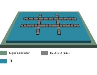
The system, as shown in Fig. 1, consists of a thin-film MTI placed on the top of an s-wave superconductor. Electric gates on top of the MTI control the top-surface electrostatic potential. The Hamiltonian of the system is Chung et al. (2011)
| (1) |
where
| (2) |
and
| (3) |
is the basis of the Hamiltonian where corresponds to an up-spin electron on the top surface and corresponds to a down-spin hole at the bottom. and are Pauli matrices corresponding to the spin and the top-bottom surfaces, respectively. and are the proximity-induced Cooper-pairing interactions at the top and bottom surfaces, respectively. The pairing interaction of the bottom surface that is in contact with the superconductor is meV Peter (2015), and at the top surface, . represent the hybridization of the top and bottom surfaces of the thin–film MTI. The value of these terms for 3 quintuple layers of Bi2Se3 are meV and eVÅ2 Zhang et al. (2017, 2010). The quantity eVÅ is consistent with DFT results Liu et al. (2010). is the Hund’s rule coupling from the ferromagnetic exchange interaction induced by the Cr dopants. For calculations using a fixed , the value is meV. The chemical potential . The last term in Eq. (3) represents the gate voltage applied at the top surface of the MTI, with the bottom surface adjacent to the superconductor at ground. An equivalent approach would be to shift by in Eq. (1) and apply the gate voltage symmetrically across the top and bottom layers such that the bottom layer is shifted to and the top layer is shifted to . This latter approach is the way the gate voltage was included in recent work Zeng et al. (2018).
To model finite and spatially varying structures, the Hamiltonian is transformed into a tight–binding model on a square lattice by substituting and in Eq. (1) and discretizing the derivatives using a 1 nm discretization length Gershoni et al. (1993). Each site in the tight-binding model is then represented by an matrix corresponding to Eq. (1) with the inter–site matrix elements coming from the discretized derivatives. Eigenenergies and eigenstates of the discretized, spatially–varying systems are calculated numerically using a Lanczos algorithm. The eigenstate calculations use periodic boundary conditions, and the simulation domain is sufficiently large that the gated regions in the neighboring cells do not interact with each other. Simulation domains are illustrated in Figs. 3(a,b) and 4(a,b).
For the calculation of conductance shown in Fig. 2(d), the transmission is determined in the usual way from the ‘device’ Green’s function and the lead self-energies Lake et al. (1997). In the calculation of the lead self energies, an imaginary potential with meV is placed on the diagonal of the discretized to assist convergence of the surface Green’s function. The zero–temperature, two–terminal conductance is then where is the transmission coefficient at the Fermi energy.
To investigate a single edge mode of a semi-infinite plane ( and ) as shown in Fig. 2(b,c), only the substitution is made, and the derivative is discretized on the 1 nm grid. Since the edge of the half-plane is parallel to , remains a good quantum number. The Hamiltonian then becomes a semi-infinite, one-dimensional chain model, where each site of the chain is represented by a –dependent matrix. The edge Green’s function is calculated using the decimation method Sancho et al. (1985); Galperin et al. (2002). Note that this is traditionally referred to as the ‘surface Green’s function,’ however, for this system, the ‘surface’ is an ‘edge.’ To resolve the edge spectrum, the energy broadening used in the calculation of the surface Green’s function is 1 meV, which is chosen to be five times larger than the energy discretization step size. The spectral function at the edge site is .
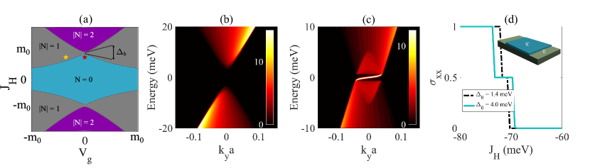
In the superconducting Nambu space, the topological superconducting Chern number (TSC), , is allowed to be where characterizes the number of chiral edge modes Wang et al. (2015). One practical way to tune the TSC number is to apply an out-of-plane external electric field to modify the top-surface electrostatic potential energy Wang et al. (2015); Zeng et al. (2018). The topological phase diagram of the system represented by Eq. (1) is plotted in Fig. 2(a) as a function of the top-gate potential and the magnitude of the exchange energy . The phase boundaries are obtained by the gap closing in the BdG Hamiltonian (Eq. (1)) at . To determine the the TSC number in each region, we evaluate the number of edge states from the bandstructure calculation of a 150 nm wide ribbon that is periodic along . is the number of the degeneracy of the edge states along one edge. The ribbon width is chosen to be sufficiently wide such that the hybridization of the edge states is negligible. The blue area belongs to the trivial phase () of a normal insulator. The purple regions correspond to , which is topologically equivalent to a non-superconducting quantum anomalous Hall insulator with Chern number . In the grey areas, , and a single Majorana edge mode propagates along the edges. As shown in Fig. 2(a), when is zero, only occurs over a narrow range of exchange potentials. Therefore, gating the top surface can control the transition between different topological phases.
To demonstrate the voltage-controlled topological transition, we numerically calculate the edge-state spectrum of the semi-infinite plane at different values of . A semi-infinite plane is chosen to ensure that the edge state hybridization is zero since the opposite edge is at . Choosing the parameters for and as shown by the two points in Fig. 2(a), the edge spectral function is plotted versus and in Figs. 2(b) and (c), respectively. In Fig. 2(b) the applied voltage is zero, , and a trivial gap opens at the Dirac point. Applying a potential to the top surface, a topological transition occurs, and a gapless Majorana edge mode appears as shown in Fig. 2(c).
For further verification of the model, we construct a 2-terminal, finite-width device consisting of a central superconducting / MTI bilayer region with two non-superconducting, topological insulator leads mimicking the experimental setup recently reported Wang et al. (2015). The structure is illustrated in the inset of Fig. 2(d) where the length of the superconductor area is 40 nm and the width is 100 nm. As seen in Fig. 2(d), a half-integer plateau in conductivity appears during a scan of the Hund’s-rule exchange energy , which emulates a scan of an externally applied magnetic field. This plateau is the result of a combination of normal reflection and Andreev reflection Wang et al. (2015).
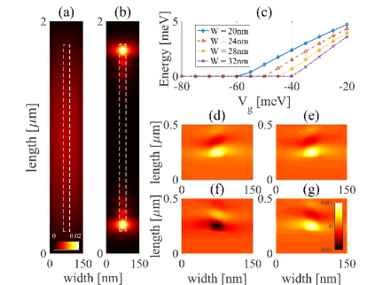
We now show that a voltage applied to a gate with a large aspect ratio can create localized Majorana zero modes at the ends. Fig. 3 shows the simulation geometry that consists of a long, thin, gated region within a rectangular supercell. The dimensions of the gated region are 28 nm 1.6 m, and the dimensions of the supercell are 150 nm 2 m. Fig. 3(a) is a color map of of the lowest positive–energy () state at each site at a gate voltage of mV. The thin width of the gated area, , is less than the penetration depth of a Majorana edge mode. This hybridizes the states on the opposing long edges of the gated region, so that a gap is opened in the energy spectrum and there is no zero–energy mode along the edges. Further decreasing to -50 mV, a pair of bound states appear at the ends of the gate as shown in Fig. 3(b), and the energy of these bound states drops 5 to 6 orders of magnitude from 5 meV to eV, suggesting that they are MZMs. The hybridization of the MZMs at the ends of the gated regions is negligible since they are 1.6 m apart.
The voltage at which the MZMs appear depends on the geometry of the gated region. Fig. 3(c) shows a calculation of the ground state energy as a function of the gate voltage for 4 different gate widths. The gate lengths are fixed at 1.6 m. For each gate width, there is a critical gate voltage at which the ground-state energy goes to zero. The magnitude of required to achieve the zero-energy state increases as the gate width decreases.
To confirm that the localized end-modes are indeed MZMs and not simply very low-energy states, the eigenvectors of the zero-modes are analyzed to determine if they satisfy the property . The eight coefficients of each mode at each site can be divided into four groups with each of the groups containing a pair of coefficients that are complex-conjugate, as shown in Eq. (4).
| (4) | ||||
is the wave function of a MZM, and , are the site–dependent normalization coefficients. The real and imaginary parts of and are shown in Fig. 3(d)-(g). Numerically, and are identical, whereas and have different signs, which satisfies Eq. (4). Similar results are obtained for the other bases. This confirms that the zero–energy states are MZMs.
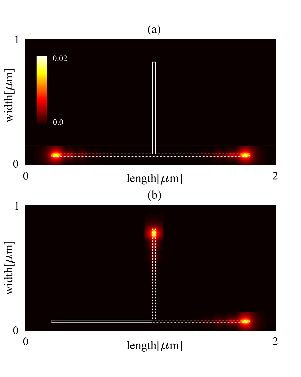
The motivation for an array of crossbar gates is to mimic a 1D network of wires for gate–controlled transfer and exchange of MZMs. A fundamental building block of such a network is a T–junction as shown in Fig. 4. With voltage applied to the horizontal section of the gate, two MZMs are created at the ends of the I-shaped gated area. Turning off the voltage of the left side gate and applying it to the vertical gate results in the MZM at the end of the ‘L’. The MZM does not appear at the sharp corner of the ‘L’. Controlling the voltages of the gates moves the topological regions () and the associated MZMs. Such a network of top gates can implement a pixel-by-pixel control of the geometric shape of the topological region, such that more complicated braiding operations can be achieved within this scheme.
All of the calculations presented are for 3 quintuple layers. In terms of the model Hamiltonian (3), only the interlayer hybridization terms, and , change due to layer thickness. For example, at 5 quintuple layers, their values become meV and eVÅ2 Zhang et al. (2010). The phase diagram of the topological transitions shown in Fig. 2(a) does not change. This means that the optimum value for is approximately , or, in other words, the spin-splitting due to the magnetic exchange interaction from the Cr dopants should be close to the hybridization gap induced by the inter-surface coupling of the top and bottom layers.
For the two dimensional system represented by Eqs. (1) - (3) with , the energy gap at is where with . Ignoring the terms since , at , the gap as seen in Fig. 2(b). The voltage required to close the gap at is mV, which scales with . When is applied in a ribbon geometry, the hybridization of the two states along the long edges of the ribbon effectively increases the parameter , which necessitates larger gate voltages to drive the initial energy gap to zero, as seen in Fig. 3(c).
Once the bands invert, they take on the Mexican hat shape, the energy gap moves away from , and its value is determined by the proximity induced Cooper pairing potential, . This is the energy gap in which the edge state resides seen in Fig. 2(c), and it is also the gap in which the MZMs reside. The MZMs are confined at a topological domain wall with the energy barriers determined by , , and . Underneath the gated ribbon, the energy spectrum is gapped by the hybridization energy of the two edge modes. Outside of the ribbon in the ungated region, the trivial energy gap confines the MZMs. The energy gaps affect the spatial extent of the MZM wavefunctions. As they are reduced, the increased tunneling necessitates wider and longer gate regions and greater separation between the gates. As is reduced, lower temperatures would be required to maintain the magnetic ordering. Thus, thicker films with lower inter-surface hybridization require smaller exchange coupling, and allow lower voltage operation, but at the cost of lower temperatures and larger areas.
In summary,
a gated MTI / superconductor bilayer provides a platform for 2D spatial control of Majorana zero modes.
The phase diagram of the system shows that a gate voltage can control the topological transition
between the and states.
The voltage of the transition depends on the gate width, and narrower gates require larger voltages.
Relatively long gates are required, approximately 2 m, to prevent hybridization of the end modes
and to allow the creation of MZMs at low gate voltages.
The MZM positions can be
controlled by the local gating of the top surface.
This scheme may provide a facile method for implementing quantum gates for topological quantum computing.
Acknowledgements: This work was supported by the National Science Foundation under Award NSF EFRI-1433395 2-DARE: Novel Switching Phenomena in Atomic Heterostructures for Multifunctional Applications and in part by FAME, one of six centers of STARnet, a Semiconductor Research Corporation program sponsored by MARCO and DARPA..
References
- Majorana and Maiani (2006) E. Majorana and L. Maiani, in Ettore Majorana Scientific Papers (Springer, Berlin, Heidelberg, 2006), pp. 201–233, ISBN 978-3-540-48091-4 978-3-540-48095-2, dOI: 10.1007/978-3-540-48095-2_10.
- Kitaev (2001) A. Y. Kitaev, Physics-Uspekhi 44, 131 (2001), ISSN 1063-7869.
- Fu and Kane (2008) L. Fu and C. L. Kane, Physical Review Letters 100, 096407 (2008).
- Wimmer et al. (2010) M. Wimmer, A. R. Akhmerov, M. V. Medvedyeva, J. Tworzydło, and C. W. J. Beenakker, Phys. Rev. Lett. 105, 046803 (pages 4) (2010).
- Elliott and Franz (2015) S. R. Elliott and M. Franz, Rev. Mod. Phys. 87, 137 (2015).
- Mourik et al. (2012) V. Mourik, K. Zuo, S. M. Frolov, S. R. Plissard, E. P. a. M. Bakkers, and L. P. Kouwenhoven, Science 336, 1003 (2012), ISSN 0036-8075, 1095-9203.
- Deng et al. (2016) M. T. Deng, S. Vaitiekėnas, E. B. Hansen, J. Danon, M. Leijnse, K. Flensberg, J. Nygård, P. Krogstrup, and C. M. Marcus, Science 354, 1557 (2016), ISSN 0036-8075, 1095-9203.
- Alicea et al. (2011) J. Alicea, Y. Oreg, G. Refael, F. v. Oppen, and M. P. A. Fisher, Nature Physics 7, 412 (2011), ISSN 1745-2481.
- Kitaev (2003) A. Y. Kitaev, Annals of Physics 303, 2 (2003), ISSN 0003-4916.
- Alicea (2012) J. Alicea, Reports on Progress in Physics 75, 076501 (2012), ISSN 0034-4885.
- Aasen et al. (2016) D. Aasen, M. Hell, R. V. Mishmash, A. Higginbotham, J. Danon, M. Leijnse, T. S. Jespersen, J. A. Folk, C. M. Marcus, K. Flensberg, et al., Physical Review X 6, 031016 (2016).
- Plissard et al. (2013) S. R. Plissard, I. v. Weperen, D. Car, M. A. Verheijen, G. W. G. Immink, J. Kammhuber, L. J. Cornelissen, D. B. Szombati, A. Geresdi, S. M. Frolov, et al., Nature Nanotechnology 8, 859 (2013), ISSN 1748-3395.
- Hell et al. (2017) M. Hell, M. Leijnse, and K. Flensberg, Phys. Rev. Lett. 118, 107701 (pages 6) (2017).
- He et al. (2017) Q. L. He, L. Pan, A. L. Stern, E. C. Burks, X. Che, G. Yin, J. Wang, B. Lian, Q. Zhou, E. S. Choi, et al., Science 357, 294 (2017), ISSN 0036-8075, 1095-9203.
- Lian et al. (2016) B. Lian, J. Wang, and S.-C. Zhang, Physical Review B 93, 161401 (2016).
- Wang et al. (2015) J. Wang, Q. Zhou, B. Lian, and S.-C. Zhang, Physical Review B 92, 064520 (2015).
- Chen et al. (2017) C.-Z. Chen, J. J. He, D.-H. Xu, and K. T. Law, Physical Review B 96, 041118 (2017).
- Sun et al. (2016) H.-H. Sun, K.-W. Zhang, L.-H. Hu, C. Li, G.-Y. Wang, H.-Y. Ma, Z.-A. Xu, C.-L. Gao, D.-D. Guan, Y.-Y. Li, et al., Physical Review Letters 116, 257003 (2016).
- Kim et al. (2016) Y. Kim, T. M. Philip, M. J. Park, and M. J. Gilbert, Phys. Rev. B 94, 235434 (pages 15) (2016).
- Zeng et al. (2018) Y. Zeng, C. Lei, G. Chaudhary, and A. H. MacDonald, Physical Review B 97, 081102 (2018).
- Chen et al. (2018) C.-Z. Chen, Y.-M. Xie, J. Liu, P. A. Lee, and K. T. Law, Phys. Rev. B 97, 104504 (2018).
- Chung et al. (2011) S. B. Chung, X.-L. Qi, J. Maciejko, and S.-C. Zhang, Physical Review B 83, 100512 (2011).
- Peter (2015) M. S. Peter, Tunneling Spectroscopy on Electron-Boson Interactions in Superconductors (KIT Scientific Publishing, 2015), ISBN 978-3-7315-0238-8.
- Zhang et al. (2017) J.-M. Zhang, R. Lian, Y. Yang, G. Xu, K. Zhong, and Z. Huang, Scientific Reports 7, 43626 (2017), ISSN 2045-2322.
- Zhang et al. (2010) Y. Zhang, K. He, C.-Z. Chang, C.-L. Song, L.-L. Wang, X. Chen, J.-F. Jia, Z. Fang, X. Dai, W.-Y. Shan, et al., Nature Physics 6, 584 (2010), ISSN 1745-2481.
- Liu et al. (2010) C.-X. Liu, X.-L. Qi, H. Zhang, X. Dai, Z. Fang, and S.-C. Zhang, Physical Review B 82, 045122 (2010).
- Gershoni et al. (1993) D. Gershoni, C. H. Henry, and G. A. Baraff, IEEE J. Quantum Electron. 29, 2433 (1993).
- Lake et al. (1997) R. Lake, G. Klimeck, R. C. Bowen, and D. Jovanovic, J. Appl. Phys. 81, 7845 (1997).
- Sancho et al. (1985) M. P. L. Sancho, J. M. L. Sancho, and J. Rubio, J. Phys. F 15, 851 (1985).
- Galperin et al. (2002) M. Galperin, S. Toledo, and A. Nitzan, J. Chem. Phys. 117, 10817 (2002).