Optical and Electronic Properties of Doped -type CuI: Explanation of Transparent Conductivity from First Principles
Abstract
We report properties of the reported transparent conductor CuI, including the effect of heavy -type doping. The results, based on first principles calculations, include analysis of the electronic structure and calculations of optical and dielectric properties. We find that the origin of the favorable transparent conducting behavior lies in the absence in the visible of strong interband transitions between deeper valence bands and states at the valence band maximum that become empty with -type doping. Instead, strong interband transitions to the valence band maximum are concentrated in the infrared with energies below 1.3 eV. This is contrast to the valence bands of many wide band gap materials. Turning to the mobility we find that the states at the valence band maximum are relatively dispersive. This originates from their antibonding Cu - I character. We find a modest enhancement of the Born effective charges relative to nominal values, leading to a dielectric constant =6.3. This is sufficiently large to reduce ionized impurity scattering, leading to the expectation that the properties of CuI can be still can be significantly improved through sample quality.
I Introduction
Transparent conductors (TCs), such as the transparent conducting oxides (TCOs), are compounds that combine low visible light absorption with high electrical conductivity.Chopra et al. (1983); Stadler (2012) They are important for opto-electronic devices including solar cells and displays, as well as for applications such as smart windows. Ginley and Bright (2000); Kawazoe et al. (2000); Ishikawa et al. (2009); Nomura et al. (2004); Chiang et al. (2005) Remarkably, in spite of industrial interest and extensive research, the number of established high performance TCs suitable for applications is relatively small. These include -type oxides based on In, especially Sn doped In2O3, Hartnagel et al. (1995); Minami (2008) -type stanates including BaSnO3, Wang et al. (2007); Sallis et al. (2013); Mizoguchi et al. (2013); Singh et al. (2014); Li et al. (2015) ZnO based materials Thomas (1960) and In-Ga-Zn oxides. Nomura et al. (2004)
Good -type TCs are less common, but are enabling for some applications, for example in transparent electronics. However, these -type materials generally have lower performance than state-of-the-art -type TCOs. This fact has motivated several studies of potential -type TCs, leading to the discovery of several new -type TC materials. Known -type TCs include, for example, Cu+ oxidesKawazoe et al. (1997); Duan et al. (2000); Ueda et al. (2000); Nagarajan et al. (2001), Sn2+ compoundsLi et al. (2016); Behrendt et al. (2015); Fortunato et al. (2010); Caraveo-Frescas et al. (2013), BaSnO3,Kim et al. (2016); Li et al. (2017) and Ba2BiTaO6.Bhatia et al. (2015)
Recently, CuI has been identified as a good -type TC material. Yang et al. (2016a, 2017); Grundmann et al. (2013); Wang et al. (2011); Chen et al. (2010); Schein et al. (2013) CuI has a cubic structure and is also compatible with solar cells and amenable to thin film growth, including growth on glass. Grundmann et al. (2013); Lee et al. (2008); Zhou et al. (2012); Yang et al. (2016b); Zhu and Zhao (2011) Here we present a first principles study of its properties as related to TC behavior, especially the issue of simultaneous conductivity and transparency in a -type material.
We find that a key aspect is the absence of strong interband transitions in the visible when doped, combined with the particular bonding of the material, which favors both -type doping and dispersive valence bands. We do not find strongly enhanced Born effective charges that would lead to unusually high dielectric constants and screening of ionized impurities, in contrast to some other high mobility halide semiconductors. Du and Singh (2010); Ming et al. (2016) Instead we find a modest enhancement, which nonetheless provides enough screening to suggest that reported -type CuI are not near the limit for increase of mobility via sample quality improvements.
II Structure and Methods
CuI has a zinc-blende structure at temperatures below 643 K, ( phase, space group 3).Keen and Hull (1995) The ambient temperature experimental lattice parameter is = 6.058 Å,Carpentier and Nitsche (1974) and we used this value. We performed first principles calculations using the projector augmented-wave (PAW) method,Kresse and Joubert (1999) as implemented in the VASP codeKresse and Furthmüller (1996) and the general potential linearized augmented planewave (LAPW)Singh and Nordstrom (2006) method as implemented in the WIEN2k code. Blaha et al. (2001) We used these two codes because of the ability to apply the virtual crystal approximation and carry out accurate optical calculations provided in WIEN2k and the need to perform hybrid functional and dielectric calculations, which are more convenient in VASP.
We treated the 34 shells of Cu and the 55 shells of I as valence electrons with PAW pseudopotentials in our VASP calculations. These were used with kinetic energy cutoffs of 300 eV. We tested to ensure that this was adequate. The k-point meshes for sampling the Brillouin zone were at a grid spacing of 2 0.02 Å-1 or better, including the hybrid functional calculations. Born effective charges were calculated using density functional perturbation theory as implemented in VASP. We used sphere radii of 2.46 Bohr for Cu and I and basis set cut-offs, , set by the criterion = 9.0 in the LAPW calculations; here is the LAPW sphere radius of 2.46 Bohr. Spin-orbit coupling (SOC) was included in all electronic structure and optical property calculations. The spin-orbit calculation was performed in WIEN2k using the second variational approach, Singh and Nordstrom (2006) in which the relativistic problem is solved using a basis set consisting of the scalar relativisitic band states. For this purpose all occupied states, plus unoccupied states up to 5 Ry were employed.
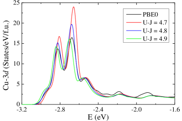
Both a correct band gap and a correct position of the Cu states in the I valence bands are important ingredients for obtaining realistic optical and transport properties. We used the generalized gradient approximation (GGA) of Perdew, Burke, and Ernzerhof (PBE), Perdew et al. (1996) and applied the GGA+U method to describe the Cu states in LAPW calculations with the WIEN2k code. Transport coefficients were obtained using the BoltzTraP code.Madsen and Singh (2006) The value of the parameter U was determined based on hybrid functional calculations with the PBE0 functional.Adamo and Barone (1999) These PBE0 calculations were done using VASP. Good agreement between the PBE0 and GGA+U calculations for the position of the Cu states was obtained for U = 4.8 eV, as shown in Fig. 1, which shows the region of the upper crystal field peak of the Cu density of states. This is the energy range that is crucial for the interband optical absorption in doped -type samples, as discussed below. Importantly, this choice of U in the GGA+U method also yields very good agreement for the shape and peak structure of the Cu density of states. Besides the good agreement between our HSE0 and GGA+U calculations for the shape and position of the Cu states, we note that these are also in good agreement with results from valence band photoemission experiments. Generalov and Vinogradov (2013)
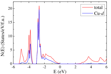

The second issue that is important for optical calculations is the band gap. Calculation of the band gap in CuI is complicated by two issues, namely, self-interaction errors associated with the localized Cu electrons and correct positioning of the Cu derived conduction bands with respect to the I derived valence bands. Because of this combination the band gap is underestimated even using hybrid functionals and full self-consistent GW calculations. Pishtshev and Karazhanov (2017) This is also the case for our GGA+U calculations, as seen in Fig. 2, which shows the density of states over a wider energy range. Fig. 3 shows the relative contribution of the Cu states to the the electronic structure. One could in principle shift the band gap by applying fitted U parameters to other orbitals. However, while it is physically clear that there is a need to correct the binding of the localized Cu levels, related to self interaction errors, Perdew and Zunger (1981) there is no clear physical basis for applying U parameters to other orbitals in CuI, and in fact the remaining error is more likely associated with the density functional band gap underestimation associated with the exchange correlation potential discontinuity. Perdew and Levy (1983) Here we relied on the experimental direct gap (3.1 eV), Tennakone et al. (1998); Derenzo et al. (2002) and applied a rigid shift of the conduction bands to match it.
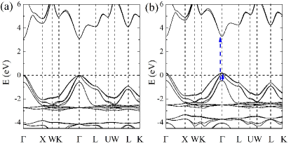
We then modeled -type CuI using the virtual crystal approximation. The virtual crystal approximation is an average potential approximation. It goes beyond rigid bands and specifically includes composition dependent distortions of the band structure, although in the present case these distortions are weak. Fig. 4 shows the band structure from the hybrid functional calculations, with the shift to reproduce the experimental gap, compared with the virtual crystal band structure at 0.025 holes per formula unit. Optical properties and plasma frequencies were calculated using the optical package of WIEN2k, using virtual crystal band structures, obtained for each doping level. In this code, the plasma frequency tensor is calculated as an integral over the Fermi surface of the square band velocity (related to diagonal momentum matrix elements). Ambrosch-Draxl and Sofo (2006) We also did rigid band calculations for the transport related properties using BoltzTraP. This calculation differs from the plasma frequency calculation in that it does not include distortions of the band structure from changes in the electron count. These distortions are included in the virtual crystal approximation, but not in the rigid band approximation. Furthermore BoltzTraP uses an analytic expression for the band velocity based on a very fine grid Fourier interpolation of the energy eigenvalues, different from the optical package of WIEN2k. We find that for CuI the rigid transport calculations yield similar results to the virtual crystal approximation for the plasma frequency.
III Results and Discussion
The band structure (Fig. 4, shown for 0.025 holes per Cu, i.e. =4.5x1020 cm-3 in the right panel), illustrates one of the main conundrums in TC materials: a TC must be both transparent and conducting at the same time under the same conditions. The band gap of CuI, as is known from experiment, is 3.1 eV, meaning that intrinsic CuI of sufficient quality should be transparent for almost all of the visible spectrum. It is also known from experiment and expected from the chemistry of compounds of monovalent Cu that the compound naturally forms -type and can be relatively easily -type doped, and then becomes conducting. The band structure shows dispersive bands at the valence band maximum (quantified below in terms of a transport effective mass) consistent with reasonable conduction.
The dispersive nature of the bands arises because, as seen in the density of states, they have antibonding Cu - I character, similar to other semiconductors. Williamson et al. (2017) This is clearly seen in the density of states, and in particular the Cu contribution (Fig. 3). The antibonding I - Cu nature of the states at the top of the valence band causes them to be higher in energy that a pure I valence band would be, leading to increased disperion as has been discussed in other compounds. Williamson et al. (2017)
The problem is that conduction requires doping. CuI, like many materials shows several bands near the valence band maximum, including the energy range from -3.25 eV to -1.65 eV, which corresponds to the visible. -type doping introduces empty states at the valence band maximum, and then one may anticipate transitions from the deeper bands to the empty states, with associated absorption of visible light. In known high performance -type TCOs, e.g. In2O3, BaSnO3 and ZnO, there are no conduction bands with energies that would allow direct transitions in the visible from the conduction band minimum. Mryasov and Freeman (2001); Singh et al. (1991); Janotti and Van de Walle (2009) Thus, while undoped CuI is expected to transparent due to the band gap, and doped CuI is expected to conduct due to the dispersion of the bands at the valence band maximum, it may at first sight be unclear how doped CuI can retain transparency.
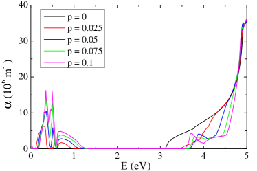
We begin with the optical properties of -type CuI, based on virtual crystal calculations that explicitly include doping induced empty states at the top of the valence bands and transitions into these states. Fig. 5 shows the absorption spectra for different -type doping levels based on interband transitions. For zero doping there is a strong absorption edge at the direct band gap due to dipole allowed transitions from the valence band maximum to the conduction band minimum. These transitions are removed by -type doping as the initial states become unoccupied. This is basically a Burstein-Moss shift. The strong absorption feature above the gap comes from the second split off hole band for heavily doped material, as shown, while additional strong absorption in the infrared appears from interband transitions within the valence bands. In addition to the interband transitions, there will be a Drude component, which depends on the doping dependent plasma frequency (see below) and the usually sample dependent scattering rate. This will yield additional infrared absorption, which we do not include.
As mentioned, undoped CuI is a semiconductor with a direct band gap and onset of absorption at 3.1 eV. Doping introduces additional strong absorption peaks in the infrared (1.3 eV) due to interband transitions. This is in contrast to many -type TCOs, such as ITO, ZnO, and BaSnO3, and reflects the availability of valence bands to participate in transitions to empty states at the valence band maximum. Thus, -type CuI is not transparent for infrared light.
The key present finding of our study as regards optical properties is that there are no significant interband transitions in the visible part of the spectrum for -type CuI. The origin is in the gap at between the upper crystal field level and the valence band maximum, as well as weak matrix elements between the states and the top valence band near (note that the symmetry of the four fold degenerate state at the valence band maximum is the same as the top Cu d band at ). This is qualitatively similar to what was recently found for another recently discovered -type TCO, KxBa1-xSnO3. Kim et al. (2016); Li et al. (2017) The TC behavior of -type CuI depends on this feature of its band structure.
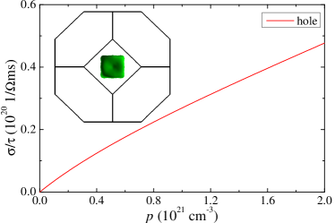
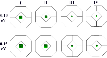
Fig. 4 shows the band structure with -type CuI, comparing the hybrid functional and PBE+U calculations (both with the conduction band shift to reproduce the experimental band gap). The virtual crystal band structure shown in the right panel is at a carrier concentration of 0.025 holes per Cu ( = 4.5 1020 cm-3). The solid vertical arrows in the band structure plot indicate the main transitions in the infrared, which are between bands below the valence band maximum and the top band. The dashed arrow indicates the transition between valence bands and conduction bands with energy 3.5 eV as seen in Fig. 5.
The valence band maximum at is four fold degenerate (including spin), as is common to most zinc-blende semiconductors. The fact that I (=53) is a heavy p-electron element, combined with the fact that the crystal structure is non-centrosymmetric, with significantly different atoms on the two sites (Cu and I), results in tiny but non-negligible spin-orbit splittings of these bands as one moves away from , so that the top four bands are formally distinct, though neglecting these spin splittings away from they are simply the heavy hole and light hole band characteristic of zinc-blende semiconductors such as GaAs.
There is an additional hole band starting 0.6 eV below the valence band maximum. This two fold degenerate (including spin) band is split from the valence band maximum by spin orbit. It is similar to the corresponding band in GaAs, but the splitting is larger due to the higher atomic number of I, relative to As. The splitting of 0.6 eV is comparable to that found in GaSb ( 0.7 eV), containing Sb (=51). Madelung (2004); Gmitra and Fabian (2016) This band ordering is in accord with experimental data. Madelung (2004); Goldmann (1977) Importantly, transitions from this lower split off band to the valence band maximum are dipole allowed in the non-centrosymmetric zinc-blende structure. The symmetry breaking from diamond structure is strong in CuI because of the very different chemical natures of Cu and I.
The other key property of a good TC is high conductivity. In practice, doping is essential for increasing the conductivity of TCO thin films, but usually heavy carrier concentration reduces the transparency. Experimentally, in samples produced so far, the transmittance of CuI is reported to reach 72% at a conductivity level of 280 Scm-1.Yang et al. (2016a) Here we use the quantity / ( is conductivity, and is an effective scattering time) to characterize the transport properties of -type CuI. This quantity is calculated directly from the band structure using the linearized Boltzmann transport theory with the relaxation time approximation, as implemented in the BoltzTraP code. Fig. 6 shows this quantity as a function of doping level, based on the rigid band approximation as determined using the BoltzTraP code. As seen, increases roughly linearly with carrier concentration (characteristic behavior of a parabolic band semiconductor) at low carrier concentration. In comparing different materials it is conventional to map the properties onto a single parabolic band model, even in cases such as CuI where there are multiple bands at the valence band maximum. This allows, for example, comparison of an effective mass between different compounds, with low effective mass indicating likelihood of good mobility and conductivity when doped. Bhatia et al. (2015) Matching the calculated to a single parabolic band model, we obtain a transport effective mass of = 0.77 ( is the mass of the electron) for carrier concentrations up to the cm-3 level, and then increasing weakly to 1.05 for cm-3. This carrier concentration dependence shows the non-parabolicity of the bands. Non-parabolicity with increasing mass away from point valence band maxima, especially for the light hole band is a characteristic of zinc-blende semiconductors consistent with what we find, e.g. along -. Kane (1957)
As mentioned, while it is useful to compare materials based on a transport effective mass, the valence band structure of -CuI does not show a single parabolic band at the band edge, and even considering a two band model with a light and heavy hole band, one may see substantial non-parabolicity. We show the isoenergy surface of the top band for a -type doping of 0.025 holes per Cu in the inset of Fig. 6. Carrier pockets for the top four bands, comprising the spin orbit split heavy and light hole bands are shown for different Fermi levels in Fig. 7. For isolated non-interacting parabolic bands with cubic symmetry these would be a simple spheres. Clearly the shapes deviate strongly from spheres particularly for the heavy hole bands. This is a consequence of the momentum dependent splitting of the bands at the valence band maximum as one moves away from the -point. The result of this type of complexity is generally a decoupling of the transport and density of states effective masses in a way that lowers the transport effective mass, and is therefore favorable for the mobility. Mecholsky et al. (2014); Xing et al. (2017) It is also to be noted that the two light hole bands have more spherical isosurfaces. The average mass of these two light hole bands is 0.25 , and actually varies between 0.23 and 0.28 , depending on direction, again reflecting the anisotropy of the carrier pockets.
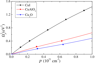
The calculated 0 K plasma frequencies, , as a function of doping level, are given in Fig. 8 along with those of CuAlO2 and Cu2O. These were obtained using the virtual crystal approximation, done by lowering the atomic number of Cu to model -type doping due to Cu vacancies, known to be important sources of -type conduction in those materials. Conductivity in metals and degenerately doped semiconductors depends on the plasma frequency, , where is an effective inverse scattering rate (at 0 K, ). As shown in Fig. 8, the plasma frequency for CuI is significantly higher than CuAlO2, consistent with good TC performance, and perhaps better performance than CuAlO2 depending on the scattering rate. It is also important to note that the doping dependence of the virtual crystal plasma frequency and that of rigid band for CuI are very similar, supporting a postiori the use of these approximations.
The reported experimental temperature dependent resistivity of heavily -type degenerate doped CuI is consistent with a resistivity that is dominated by defect scattering, especially ionized impurity scattering and grain boundary scattering rather than electron phonon scattering. Yang et al. (2016a) As such, the question arises as to the extent to which the scattering can be improved, e.g. by improvements in sample quality. Some level of ionized impurity scattering is inevitable in heavily doped bulk semiconductors as a result of the dopants. This sets an upper limit on the conductivity. This limit is very sensitive to the dielectric constant. Shuai et al. (2017); Sun and Singh (2017) In the case where only ionized impurity scattering applies the mobility, , varies as the square of the static zero frequency dielectric constant. Debye and Conwell (1954)
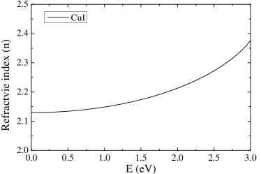
Our optical calculations without doping and including only the electronic response yield a low frequency refractive index, =2.13, which is in good agreement with literature values, =2.14 (Ref. Ageev et al., 1974) and =2.20 (Ref. Potts et al., 1973). The energy dependence is shown in Fig. 9. Our low energy value corresponds to an optical dielectric constant, =4.53.
Ionized impurity scattering is, however, governed by the static dielectric constant, including the lattice and electronic parts. Experimentally, CuI is invariably a -type doped semiconductor due to the presence of Cu vacancies. The resulting conductivity complicates measurements of the static dielectric constant. Literature values range from =6.5 to =15. Hanson et al. (1972); Ageev et al. (1974); Plendl et al. (1966) In addition, it should be noted that the cuprous halides, including CuI, are near a structural phase transition, reflecting borderline stability of the zinc-blende structure against a more ionic rock structure, as is seen in the pressure dependent phase transitions and in plots of structure vs. Phillips ionicity. This leads to anomalous lattice dynamics, affecting the validity of the Lynddane-Sachs-Teller relation that may otherwise be used to estimate from phonon measurements as well as properties such as thermal conductivity. Martin (1970); Hennion et al. (1972); Park and Chadi (1996); Mukhopadhyay et al. (2017)
We calculated the lattice part of the dielectric constant and the Born charges with the PBE GGA using VASP. We also calculated the electronic dielectric constant in the same way. The electronic dielectric constant from these PBE GGA calculations was 4.77, slightly larger than from the PBE+U calculations with WIEN2k as might be anticipated in view of the lower band gap in the PBE GGA calculations. The difference betweem the PBE GGA and the PBE+U calculations of the electronic dielectric constant with WIEN2k (including for the PBE+U calculation the shift of the conduction bands to match the experimental gap) amounts to 5%, which implies that the effect of the density functional band gap error on the electronic dielectric constant is relatively small in CuI.
The electronic structure results show a near ionic situation, with occupied I bands, and states near the conduction band minumum having Cu character. As such one may write a nominally ionic model, Cu+I-, with nominal charges 1 on the two ions. We obtained calculated Born charges 1.10, i.e. weakly enhanced from these nominal values of 1. Such an enhancement in the zinc-blende structure is unusual, and presumably reflects the significant ionicity of the compound combined with cross gap hybridization between the I derived orbitals in the valence bands and the Cu states in the conduction bands, consistent with a recent discussion of the bonding based on first principles calculations. Pishtshev and Karazhanov (2017) However, the enhancement of the Born charges in CuI is not large enough to lead to a large enhancement of the dielectric constant. Our calculated value is =6.3, which is at the lower end of the literature experimental values, supporting the direct low temperature electrical measurements of Hanson and co-workers. Hanson et al. (1972) It should be noted, however, that while smaller than the dielectric constant of high performance halide semiconductors, such as TlBr or the Pb halide perovskite solar absorbers, Du and Singh (2010); Ming et al. (2016) it is still sufficient that the limit on the mobility due to ionized impurity scattering is well below reported values. For example, Grundmanm and co-workers Grundmann et al. (2013) report a mobility fit to the Shockley expression for a degenerate semiconductor and obtain a constant of 0.25 . Here is the coefficient for the scattering rate for electrons of mass with dielectric constant unity. Within such models the scattering rate is proportional to the mass and inversely proportional to the square of the dielectric constant. Our dielectric constant of 6 would leave room for a very substantial improvement. While this is a very crude estimate and it ignores other sources of scattering, including the unavoidable electron-phonon scattering, it does still imply that substantial improvement in the mobility remains possible from improvement in sample quality. Furthermore, we note that the relatively modest dielectric constant of CuI suggests that there may be room for improving the electrical properties by for example alloying as in other cases. Williamson et al. (2017) Alloying to increase the value of has discussed and shown experimentally to be effective for another material. Shuai et al. (2017) We do, however, note that alloying involves alloy scattering and increased possibilities for defects, which may work against the mobility.
IV Summary and Conclusions
We present first principles calculations of optical and electronic properties of -type CuI, explaining the nature of its high transparency and conductivity. The calculations show that although -type doping of CuI produces strong optical absorption in the infrared below 1.3 eV, high transparency in the visible is retained due to the specific band structure. We also find a band structure consistent with reasonable conduction based on the calculated transport functions. The high visible transparency of doped CuI is a characteristic that depends on the details of the electronic structure and goes beyond the often quoted requirements of low effective mass and sufficient band gap for transparent conductors. In addition we find a dielectric constant that while smaller than other high performance halide semiconductors is nonetheless large enough to imply that the mobility of CuI samples reported in literature can still be substantially improved by improvements in sample quality.
Acknowledgements.
This work was supported by the Department of Energy through the S3TEC Energy Frontier Research Center, Award DE-SC0001299/DE-FG02ER46577.References
- Chopra et al. (1983) K. Chopra, S. Major, and D. Pandya, Thin solid films 102, 1 (1983).
- Stadler (2012) A. Stadler, Materials (Basel) 5, 661 (2012).
- Ginley and Bright (2000) D. S. Ginley and C. Bright, MRS Bull. 25, 15 (2000).
- Kawazoe et al. (2000) H. Kawazoe, H. Yanagi, K. Ueda, and H. Hosono, MRS Bull. 25, 28 (2000).
- Ishikawa et al. (2009) F. N. Ishikawa, H.-K. Chang, K. Ryu, P.-C. Chen, A. Badmaev, L. Gomez De Arco, G. Shen, and C. Zhou, ACS Nano 3, 73 (2009).
- Nomura et al. (2004) K. Nomura, H. Ohta, A. Takagi, T. Kamiya, M. Hirano, and H. Hosono, Nature 432, 488 (2004).
- Chiang et al. (2005) H. Q. Chiang, J. F. Wager, R. L. Hoffman, J. Jeong, and D. A. Keszler, Appl. Phys. Lett. 86, 013503 (2005).
- Hartnagel et al. (1995) H. L. Hartnagel, A. L. Dawar, A. K. Jain, and C. Jagadish, Semiconducting transparent thin films (Institute of Physics, Bristol, 1995).
- Minami (2008) T. Minami, Thin Solid Films 516, 5822 (2008).
- Wang et al. (2007) H. F. Wang, Q. Z. Liu, G. Y. Gao, and W. Wu, J. Appl. Phys. 101, 106105 (2007).
- Sallis et al. (2013) S. Sallis, D. O. Scanlon, S. C. Chae, N. F. Quackenbush, D. A. Fischer, J. C. Woicik, J. H. Guo, S. W. Cheong, and L. F. J. Piper, Appl. Phys. Lett. 103, 042105 (2013).
- Mizoguchi et al. (2013) H. Mizoguchi, P. Chen, P. Boolchand, V. Ksenofontov, C. Felser, P. W. Barnes, and P. M. Woodward, Chem. Mater. 25, 3858 (2013).
- Singh et al. (2014) D. J. Singh, Q. Xu, and K. P. Ong, Appl. Phys. Lett. 104, 011910 (2014).
- Li et al. (2015) Y. Li, L. Zhang, Y. Ma, and D. J. Singh, APL Mater. 3, 011102 (2015).
- Thomas (1960) D. G. Thomas, J. Phys. Chem. Solids 15, 86 (1960).
- Kawazoe et al. (1997) H. Kawazoe, M. Yasukawa, H. Hyodo, M. Kurita, H. Yanagi, and H. Hosono, Nature 389, 939 (1997).
- Duan et al. (2000) N. Duan, A. W. Sleight, M. K. Jayaraj, and J. Tate, Appl. Phys. Lett. 77, 1325 (2000).
- Ueda et al. (2000) K. Ueda, S. Inoue, S. Hirose, H. Kawazoe, and H. Hosono, Appl. Phys. Lett. 77, 2701 (2000).
- Nagarajan et al. (2001) R. Nagarajan, A. D. Draeseke, A. W. Sleight, and J. Tate, J. Appl. Phys. 89, 8022 (2001).
- Li et al. (2016) Y. Li, D. J. Singh, M.-H. Du, Q. Xu, L. Zhang, W. Zheng, and Y. Ma, J. Mater. Chem. C 4, 4592 (2016).
- Behrendt et al. (2015) A. Behrendt, C. Friedenberger, T. Gahlmann, S. Trost, T. Becker, K. Zilberberg, A. Polywka, P. Görrn, and T. Riedl, Adv. Mater. 27, 5961 (2015).
- Fortunato et al. (2010) E. Fortunato, R. Barros, P. Barquinha, V. Figueiredo, S.-H. K. Park, C.-S. Hwang, and R. Martins, Appl. Phys. Lett. 97, 052105 (2010).
- Caraveo-Frescas et al. (2013) J. A. Caraveo-Frescas, P. K. Nayak, H. A. Al-Jawhari, D. B. Granato, U. Schwingenschlögl, and H. N. Alshareef, ACS Nano 7, 5160 (2013).
- Kim et al. (2016) H. M. Kim, U. Kim, C. Park, H. Kwon, and K. Char, APL Mater. 4, 056105 (2016).
- Li et al. (2017) Y. Li, J. Sun, and D. J. Singh, Appl. Phys. Lett. 110, 051904 (2017).
- Bhatia et al. (2015) A. Bhatia, G. Hautier, T. Nilgianskul, A. Miglio, J. Sun, H. J. Kim, K. H. Kim, S. Chen, G.-M. Rignanese, X. Gonze, and J. Suntivich, Chem. Mater. 28, 30 (2015).
- Yang et al. (2016a) C. Yang, M. Kneiss, M. Lorenz, and M. Grundmann, Proc. Natl. Acad. Sci. (USA) 113, 12929 (2016a).
- Yang et al. (2017) C. Yang, D. Souchay, M. Kneiß, M. Bogner, H. Wei, M. Lorenz, O. Oeckler, G. Benstetter, Y. Q. Fu, and M. Grundmann, Nat. Commun. 8 (2017).
- Grundmann et al. (2013) M. Grundmann, F.-L. Schein, M. Lorenz, T. Böntgen, J. Lenzner, and H. von Wenckstern, Phys. Status Solidi A 210, 1671 (2013).
- Wang et al. (2011) J. Wang, J. Li, and S.-S. Li, J. Appl. Phys. 110, 054907 (2011).
- Chen et al. (2010) D. Chen, Y. Wang, Z. Lin, J. Huang, X. Chen, D. Pan, and F. Huang, Cryst. Growth Des. 10, 2057 (2010).
- Schein et al. (2013) F.-L. Schein, H. von Wenckstern, and M. Grundmann, Appl. Phys. Lett. 102, 092109 (2013).
- Lee et al. (2008) J.-H. Lee, D.-S. Leem, and J.-J. Kim, Org. Electron. 9, 805 (2008).
- Zhou et al. (2012) Y. Zhou, T. Taima, T. Miyadera, T. Yamanari, M. Kitamura, K. Nakatsu, and Y. Yoshida, Nano Lett. 12, 4146 (2012).
- Yang et al. (2016b) C. Yang, M. Kneiß, F.-L. Schein, M. Lorenz, and M. Grundmann, Sci. Rep. 6, 21937 (2016b).
- Zhu and Zhao (2011) B. L. Zhu and X. Z. Zhao, Phys. Stat. Sol. A 208, 91 (2011).
- Du and Singh (2010) M.-H. Du and D. J. Singh, Phys. Rev. B 81, 144114 (2010).
- Ming et al. (2016) W. Ming, H. Shi, and M. H. Du, J. Mater. Chem. A 4, 13852 (2016).
- Keen and Hull (1995) D. A. Keen and S. Hull, J. Phys.: Condens. Matter 7, 5793 (1995).
- Carpentier and Nitsche (1974) C. D. Carpentier and R. Nitsche, Mater. Res. Bull. 9, 1097 (1974).
- Kresse and Joubert (1999) G. Kresse and D. Joubert, Phys. Rev. B 59, 1758 (1999).
- Kresse and Furthmüller (1996) G. Kresse and J. Furthmüller, Phys. Rev. B 54, 11169 (1996).
- Singh and Nordstrom (2006) D. J. Singh and L. Nordstrom, Planewaves, Pseudopotentials, and the LAPW method, 2nd Ed. (Springer, Berlin, 2006).
- Blaha et al. (2001) P. Blaha, K. Schwarz, G. K. H. Madsen, D. Kvasnicka, and J. Luitz, WIEN2k, An augmented plane wave+ local orbitals program for calculating crystal properties (2001).
- Perdew et al. (1996) J. P. Perdew, K. Burke, and M. Ernzerhof, Phys. Rev. Lett. 77, 3865 (1996).
- Madsen and Singh (2006) G. K. H. Madsen and D. J. Singh, Comput. Phys. Commun. 175, 67 (2006).
- Adamo and Barone (1999) C. Adamo and V. Barone, J. Chem. Phys. 110, 6158 (1999).
- Generalov and Vinogradov (2013) A. V. Generalov and A. S. Vinogradov, Phys. Sol. State 55, 1136 (2013).
- Pishtshev and Karazhanov (2017) A. Pishtshev and S. Z. Karazhanov, J. Chem. Phys. 146, 064706 (2017).
- Perdew and Zunger (1981) J. P. Perdew and A. Zunger, Phys. Rev. B 23, 5048 (1981).
- Perdew and Levy (1983) J. P. Perdew and M. Levy, Phys. Rev. Lett. 51, 1884 (1983).
- Tennakone et al. (1998) K. Tennakone, G. R. R. A. Kumara, I. R. M. Kottegoda, V. P. S. Perera, G. M. L. P. Aponsu, and K. G. U. Wijayantha, Sol. Energy Mater. Sol. Cells 55, 283 (1998).
- Derenzo et al. (2002) S. E. Derenzo, M. J. Weber, and M. K. Klintenberg, Nucl. Instrum. Methods Phys. Res., Sect. A 486, 214 (2002).
- Ambrosch-Draxl and Sofo (2006) C. Ambrosch-Draxl and J. O. Sofo, Comp. Phys. Commun. 175, 1 (2006).
- Williamson et al. (2017) B. A. D. Williamson, J. Buckeridge, J. Brown, S. Ansbro, R. G. Palgrave, and D. O. Scanlon, Chem. Mater. 29, 2402 (2017).
- Mryasov and Freeman (2001) O. N. Mryasov and A. J. Freeman, Phys. Rev. B 64, 233111 (2001).
- Singh et al. (1991) D. J. Singh, D. A. Papaconstantopoulos, J. P. Julien, and F. Cyrot-Lackmann, Phys. Rev. B 44, 9519 (1991).
- Janotti and Van de Walle (2009) A. Janotti and C. G. Van de Walle, Rep. Prog. Phys. 72, 126501 (2009).
- Madelung (2004) P. D. O. Madelung, Semiconductors: Data Handbook (Springer, Berlin, 2004).
- Gmitra and Fabian (2016) M. Gmitra and J. Fabian, Phys. Rev. B 94, 165202 (2016).
- Goldmann (1977) A. Goldmann, phys. stat. sol. (b) 81, 9 (1977).
- Kane (1957) E. O. Kane, J. Phys. Chem. Solids 1, 249 (1957).
- Mecholsky et al. (2014) N. A. Mecholsky, L. Resca, I. L. Pegg, and M. Fornari, Phys. Rev. B 89, 155131 (2014).
- Xing et al. (2017) G. Xing, J. Sun, Y. Li, X. Fan, W. Zheng, and D. J. Singh, Phys. Rev. Mater. 1, 065405 (2017).
- Shuai et al. (2017) J. Shuai, J. Mao, S. Song, Q. Zhu, J. Sun, Y. Wang, R. He, J. Zhou, G. Chen, D. J. Singh, and Z. Ren, Energy Environ. Sci. 10, 799 (2017).
- Sun and Singh (2017) J. Sun and D. J. Singh, Phys. Rev. Appl. 7, 024015 (2017).
- Debye and Conwell (1954) P. Debye and E. Conwell, Phys. Rev. 93, 693 (1954).
- Ageev et al. (1974) L. A. Ageev, V. K. Miloslavskii, and T. I. Maksimenko, Opt. Spectrosc. (USSR) 36, 76 (1974).
- Potts et al. (1973) J. E. Potts, R. C. Hanson, C. T. Walker, and C. Schwab, Solid State Commun. 13, 389 (1973).
- Hanson et al. (1972) R. C. Hanson, J. R. Hallberg, and C. Schwab, Appl. Phys. Lett. 21, 490 (1972).
- Plendl et al. (1966) J. N. Plendl, A. Hadni, J. Claudel, Y. Henninger, G. Morlot, P. Strimer, and L. C. Mansur, Appl. Opt. 5, 397 (1966).
- Martin (1970) R. M. Martin, Phys. Rev. B 1, 4005 (1970).
- Hennion et al. (1972) B. Hennion, F. Moussa, B. Prevot, C. Carabatos, and C. Schawb, Phys. Rev. Lett. 28, 964 (1972).
- Park and Chadi (1996) C. H. Park and D. J. Chadi, Phys. Rev. Lett. 76, 2314 (1996).
- Mukhopadhyay et al. (2017) S. Mukhopadhyay, D. Bansal, O. Delaire, D. Perrodin, E. Bourret-Courchesne, D. J. Singh, and L. Lindsay, Phys. Rev. B 96, 100301 (2017).