Almost ideal nodal-loop semimetal in monoclinic CuTeO3 material
Abstract
Nodal-loop semimetals are materials in which the conduction and valence bands cross on a one-dimensional loop in the reciprocal space. For the nodal-loop character to manifest in physical properties, it is desired that the loop is close to the Fermi level, relatively flat in energy, simple in its shape, and not coexisting with other extraneous bands. Here, based on the first-principles calculations, we show that the monoclinic CuTeO3 is a realistic nodal-loop semimetal that satisfies all these requirements. The material features only a single nodal loop around the Fermi level, protected by either of the two independent symmetries: the symmetry and the glide mirror symmetry. The size of the loop can be effectively tuned by strain, and the loop can even be annihilated under stain, making a topological phase transition to a trivial insulator phase. Including the spin-orbit coupling opens a tiny gap at the loop, and the system becomes a topological semimetal with a nontrivial bulk invariant but no global bandgap. The corresponding topological surface states have been identified. We also construct a low-energy effective model to describe the nodal loop and the effect of spin-orbit coupling.
I Introduction
The study of topological states of matter have been attracting significant interest in the current condensed matter physics research. Topological insulators which possess insulating bulk states and robust metallic surface states have been extensively studied Hasan and Kane (2010); Qi and Zhang (2011). Recently, topological metals and semimetals have emerged as a new research focus Chiu et al. (2016); Burkov (2016); Armitage et al. (2018). Their band structures exhibit nontrivial band crossings near the Fermi energy, around which the low-energy quasiparticles behave differently from the conventional Schrödinger-type fermions. For instance, Weyl and Dirac semimetals host isolated twofold and fourfold degenerate linear band-crossing points, respectively, where the electronic excitations are analogous to the relativistic Weyl and Dirac fermions Volovik (2003); Wan et al. (2011); Murakami (2007); Burkov and Balents (2011); Young et al. (2012); Wang et al. (2012, 2013); Zhao and Wang (2013); Yang and Nagaosa (2014); Weng et al. (2015a); Liu et al. (2014); Borisenko et al. (2014); Lv et al. (2015); Xu et al. (2015a), making it possible to simulate interesting high-energy physics phenomena in condensed matter systems Nielsen and Ninomiya (1983); Son and Spivak (2013); Guan et al. (2017a).
The conduction and valence bands may also cross along a one-dimensional (1D) loop in the Brillouin zone (BZ). Such nodal loops can be protected by symmetries and may lead to drumhead-like surface bands. Several interesting properties have been predicted for nodal-loop semimetals, such as the anisotropic electron transport Mullen et al. (2015), the unusual optical response and circular dichorism Carbotte (2016); Ahn et al. (2017); Liu et al. (2018), the possible surface magnetism and superconductivity Heikkilä et al. (2011); Li et al. (2016); Chan et al. (2016); Wang and Nandkishore (2017); Liu and Balents (2017), the anomalous Landau level spectrum Rhim and Kim (2015); Lim and Moessner (2017), and density fluctuation plasmons and Friedel oscillations Rhim and Kim (2016). Quite a few realistic materials have been proposed as nodal-loop semimetals Yang et al. (2014); Weng et al. (2015b); Mullen et al. (2015); Yu et al. (2015); Kim et al. (2015); Chen et al. (2015a, b); Fang et al. (2016); Chan et al. (2016); Bian et al. (2016); Schoop et al. (2016); Gan et al. (2017); Li et al. (2017a); Zhang et al. (2017); Huang et al. (2017); Jiao et al. (2017); Li et al. (2018), and interestingly, Dirac and Weyl loops have also been proposed in cold-atom optical lattices Xu and Zhang (2016). However, to unambiguously identify the predicted features due to the nodal loops in these systems still remains challenging, partly because the low-energy band structures of the realistic materials suffer from various drawbacks. As a good nodal-loop semimetal, the material should at least satisfy the following requirements. First, the nodal loop should be close to the Fermi level. Second, the energy variation along the loop should be as small as possible. Third, the loop has a relatively simple shape, and it is better that only a single loop appears at low-energy. Fourth, it is crucial that no other extraneous bands are nearby in energy, since otherwise they may complicate the interpretation of measured properties (like for the transport coefficients) Gao et al. (2017). Hence, to facilitate the experimental exploration of the nodal-loop semimetals, an urgent task is to identify realistic materials that satisfy these requirements.
In this work, based on first-principles calculations and symmetry analysis, we predict that the monoclinic CuTeO3 is a nodal-loop semimetal which satisfies all the above-mentioned requirements. The material features a single nodal loop close to the Fermi level in its low-energy band structure. The loop is almost flat in energy and there is no other extraneous band crossing the Fermi level. The stability of the loop is protected by either of the two independent symmetries in the absence of spin-orbit coupling (SOC): the symmetry and the glide mirror symmetry of the system. We show that lattice strain can effectively tune the shape of the loop, and even annihilate the loop to make a topological phase transition into a trivial insulator phase. SOC opens a gap at the nodal loop, and transforms the system into a topological semimetal which has a nontrivial bulk invariant but no global bandgap. The corresponding nontrivial surface states are revealed. We also construct a low-energy effective model to capture the nodal-loop as well as the effect of SOC. Since the SOC is negligible for this material, the nodal-loop features should clearly manifest in experimental measurements. Our result suggests an almost ideal platform for experimentally exploring the intriguing properties of nodal-loop semimetals.
II CRYSTAL STRUCTURE
CuTeO3 belongs to the tellurium(IV)-oxygen compounds. It may crystalize into two typical structures: the orthorhombic structure and the monoclinic structure, which are denoted as structure I and II Pertlik (1987), respectively. In this work, we focus on the monoclinic CuTeO3, which has been successfully synthesized by a hydrothermal method and shown to be stable at ambient condition Pertlik (1987). The chemical formula and the crystal structure have been determined by a quantitative analysis of the X-ray diffraction data (the crystal structure data are Å, Å, Å, and , where is the angle between and axis) Pertlik (1987).
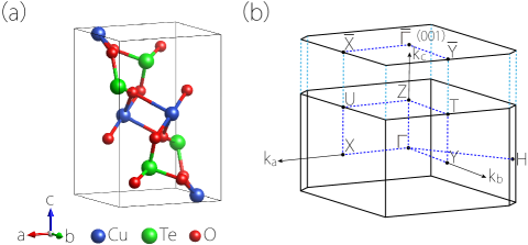
The monoclinic CuTeO3 has a structure with space group No. 14 () [see Fig. 1(a)], which can be generated by the following symmetry elements: the inversion [inversion center located at ] and the glide mirror . Here the tilde denotes a nonsymmorphic operation, which involves a translation with fractional lattice parameters. In addition, the material has been found to show no magnetic ordering Pertlik (1987), so the time reversal symmetry is also preserved. The crystal structure of monoclinic CuTeO3 and the BZ are schematically shown in Fig. 1.
III First-principles Methods
We performed first-principles calculations based on the density functional theory (DFT) using the projector augmented wave method as implemented in the Vienna ab initio simulation package Kresse and Hafner (1994); Kresse and Furthmüller (1996); Blöchl (1994). The exchange-correlation functional was modeled within the generalized gradient approximation (GGA) with the Perdew-Burke-Ernzerhof (PBE) realization Perdew et al. (1996). The cutoff energy was set as 550 eV, and the BZ was sampled with a -centered mesh of size . The experimental lattice parameters ( Å, Å, Å) Pertlik (1987) were adopted in the calculation. The band structure result was further checked by using the more accurate approach with the modified Becke-Johnson (mBJ) potential Tran and Blaha (2009). We confirm that the essential features including the nodal loop remain the same as in the GGA result (see Appendix A). As Cu() orbitals may have correlation effects, we also tested our result by using the GGA method Anisimov et al. (1991), and the results are discussed in Section V. In order to study the topological surface states, localized Wannier functions were constructed by projecting the Bloch states onto atomic-like trial orbitals without an iterative procedure Marzari and Vanderbilt (1997); Souza et al. (2001); Huang et al. (2017). Using the Wannier functions, the surface spectra were calculated via the iterative Green’s function method Gre as implemented in the WannierTools package Wu et al. (2017).
IV RESULTS
IV.1 Nodal-loop semimetal in CuTeO3
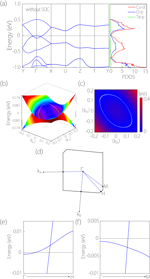
We first consider the electronic band structure of monoclinic CuTeO3 (hereafter referred to as simply CuTeO3) in the absence of SOC. The band structure from DFT calculation is shown in Fig. 2(a), along with the projected density of states (PDOS). From PDOS, one clearly observes that the system is a semimetal: it has zero bandgap but the density of states at the Fermi level is very small. The low-energy states near the Fermi level are mainly from the Cu() orbitals and the O() orbitals.
In the band structure, there appear linear band-crossing points along the Y- and -X paths very close to the Fermi level [see Fig. 2(a)]. Actually, these points are not isolated. Via a careful scan of the crossing points in the BZ, we find that the two points belong to a nodal loop centered around the point in the plane, formed by the crossing between the conduction and the valence bands. This is more clearly shown in Fig. 2(b), where we plot the dispersion of the two bands in the plane around . One directly observes that they cross along a 1D loop in this plane. The shape of the nodal loop obtained from the scan is shown in Fig. 2(c). These results demonstrate that the material is a nodal-loop semimetal with a single nodal loop close to the Fermi level in the band structure. The loop is quite flat in energy, with an energy variation less than 0.04 eV. More importantly, the band structure is clean in the sense that there is no other extraneous band near the Fermi level. Thus, CuTeO3 satisfies the conditions we listed at the Introduction section for a good nodal-loop semimetal.
Depending on the slope of the two crossing bands, a nodal point can be classified as type-I or type-II Xu et al. (2015b); Soluyanov et al. (2015). Recently, Li et al. proposed the concepts of type-II and hybrid nodal loops Li et al. (2017a), based on the type of the nodal points that make up the loop. A loop is type-I (type-II) if all the points on the loop are type-I (type-II) in the 2D transverse dimensions. If a loop contains both type-I and type-II points, then it corresponds to a hyrbid type. Several interesting physical properties have been predicted for each type of the loops Heikkilä and Volovik (2015); Hyart and Heikkilä (2016); Gao et al. ; Zhang et al. . Here, we also determine the type of the nodal loop found in CuTeO3. By scanning the dispersion around the loop, we find that although most points on the loop are of type-I [Fig. 2(f)], there are small sections of the loop where the points are of type-II [Fig. 2(e)]. Thus, the loop contains both type-I and type-II points, and according to the definition, it belongs to the hybrid type.
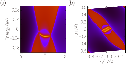
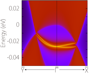
Nodal loops usually display drumhead-like surface states at the sample surface, on which the loop has a nonzero projected area Yang et al. (2014); Weng et al. (2015b). In Fig. 3, we show the spectrum for the (001) surface. One indeed observes a surface band connecting the nodal points that correspond to the loop in the bulk [see Fig. 3(a)]. And the surface states lie within the surface projected nodal loop, as seen in Fig. 3(b) for a constant energy slice at eV. It is worth noting that in Fig. 3(b), the surface states in the constant energy slice appear as open arcs, which seems peculiar as one typically expects a closed curve, as found in most previous works. However, such result is not unreasonable, because the shape of the surface states in the constant energy slice depends on the detailed dispersion of the surface band. Consider a surface band having a saddle-like shape in its dispersion, then on a constant energy slice, the surface states naturally appear as sections of hyperbolic curves (open arcs).
IV.2 Symmetry protection
The nodal loop in CuTeO3 is protected by either of the two independent symmetries: the symmetry and glide mirror symmetry , when SOC is absent.
In the absence of SOC, spin is a dummy degree of freedom, and the usual treatment is to simply drop the spin labels and the trivial spin degeneracy. Hence, for the current system, without SOC, the nodal loop can be regarded as formed by the crossing between two (spinless) bands. Then the presence of symmetry requires that the Berry phase for any closed 1D manifold to be quantized into multiples of Zhao et al. (2016). Here, the Berry phase
| (1) |
is defined for a locally gapped spectrum along a closed path , is the periodic part of the Bloch eigenstate, and the band index is summed over the occupied valence bands below the local gap. Hence, mod defines a 1D invariant. For a nodal loop, for a closed path encircling the loop is , hence protecting the loop against weak perturbations from opening a gap. In DFT calculations, we have also numerically checked that such Berry phase is nontrivial.
Another protection is from the glide mirror symmetry . The loop lies in the plane, which is invariant under . Hence, each state in this plane is also an eigenstate of , with a well-defined eigenvalue . The nodal loop is protected if the two crossing bands have opposite in the plane, which is indeed the case as verified by our DFT calculations (the conduction band has positive eigenvalues, and the valence band has negative eigenvalues). The presence of symmetry further pins the nodal loop to be within the plane.
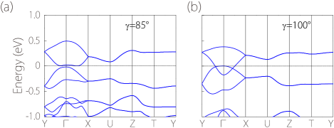
The two symmetries are independent, so the loop is protected as long as one of them is preserved. We have checked this point by making lattice distortions that break one while maintaining the other. This also offers possibility to tune the nodal loop by strain engineering. The location and the shape of the loop can be effectively tuned by strain, if the applied strain preserves one of the two symmetries. For example, let’s consider a lattice deformation by varying the angle between the and axis, corresponding to a type of shear strain. As shown in Fig. 4, one observes that the shape of the loop varies with strain, and it becomes larger when the angle is increased. Importantly, at decreased angle, the loop shrinks as the band inversion at is reduced. For , the loop is completely removed, and the system has made a topological phase transition into a trivial insulator phase.
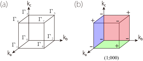
In addition, since the system preserves inversion symmetry, we can also analyze the topology of the nodal loop using the method discussed in Ref. Kim et al. (2015). In this method, we calculate the product of parity eigenvalues for the occupied states at the eight time reversal invariant momenta (TRIM) , where . The results are indicated in Fig. 5. Then we can obtain the invariant for the six invariant planes. Three of the six planes have nontrivial , as marked by the shaded regions in Fig. 5(b). This is consistent with the fact that the loop pierces through these three planes. This analysis also gives the invariant for a topological insulator once SOC is included, as we discuss in a while.
IV.3 Effect of SOC
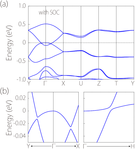
Next, we turn to the band structure with SOC. Because the low-energy states are mainly from the Cu and O atomic orbitals, the SOC effect is expected to be small since these are light elements. This is verified in the DFT calculation. The band structure with SOC is plotted in Fig. 6(a). One observes that it is quite similar to the result without SOC in Fig. 2(a). Here, each band is at least doubly degenerate due to the symmetry. This is because each point is invariant under , and with SOC, we have , leading to a Kramers-like degeneracy for each band at each point. It should be noted that even if the individual and are broken, as along as the combined symmetry holds, the double degeneracy will still be there (such as in some magnetic materials). Zooming in the crossings corresponding to the nodal loop [see Fig. 6(b)], one can see that there is a very small gap (about 0.0075 eV) opened at the original nodal loop.
After including the SOC, there is a local gap between conduction and valence bands at every point. Hence, we can have a well-defined invariant for the valence bands Pan et al. (2014); Guan et al. (2017b), just like that for the 3D topological insulators. Since band inversion occurs at the point, one naturally expects that this invariant is nontrivial. The material here has inversion symmetry, so the invariant can be conveniently evaluated by analyzing the parity eigenvalues at the TRIM points Fu and Kane (2007). This in fact has been done in the previous section (see Fig. 5), and we find that , which is indeed nontrivial. Note that there is no global bandgap for the spectrum—the bandgap is closed indirectly, so in a strict sense the system is a topological semimetal Pan et al. (2014); Guan et al. (2017b). Like topological insulators, such state also possesses spin-momentum-locked topological surface states. In Fig. 7, we show the surface spectrum for the (001) surface. Compared with the result in Fig. 3(a), one observes that the drumhead surface states are split by the SOC and evolve into the spin-polarized surface states for the topological semimetal.
Here, it should be mentioned that the SOC effect is quite small for CuTeO3. At energy scales larger than the SOC gap ( eV), the SOC effect has negligible influence on measured physical properties, and the material may be well described by a nodal-loop semimetal.
IV.4 Low-energy effective model
To further characterize the nodal-loop semimetal phase and to understand the effect of SOC, we construct a low-energy effective () model based on the symmetry requirements.
We first consider the case without SOC. The two low-energy states at the point belong to the and representations of the point group at . Using them as basis, we can obtain a two-band model that is constrained by symmetry. To capture the nodal loop, we expand the model at to leading order terms in each wave-vector component , which gives
| (2) |
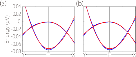
where the Pauli matrices are in the space spanned by the two basis states at , , , and . In the specified basis, the inversion and time reversal operations take the following representations: , and with the complex conjugation operation. One can easily verify that the model respects both symmetries. From this model, we find that a nodal loop would appear in the plane under the condition that . The parameters fitted from the first-principles result are eV, eVÅ2, eVÅ2, eVÅ2, eV, eVÅ2, eVÅ2, eVÅ2, and eVÅ, which satisfy the condition above. The fitting result of the band structure is shown in Fig. 8(a).
When SOC is included, there will be additional SOC terms in the Hamiltonian. Treating SOC as perturbations, we add to model in Eq. (2) the leading order symmetry-allowed SOC terms, given by
| (3) |
where the Pauli matrices stand for the real spin. Then the full model is . One easily checks that the SOC terms open a gap at the original nodal loop. For CuTeO3, the SOC strength is small, so the gap is also negligible. The parameters obtained from fitting the first-principles result are eVÅ, eVÅ, eVÅ, eVÅ, eVÅ. The fitting result for the band structure with SOC is shown in Fig. 8(b).
V Discussion and Conclusion
Based on their formation mechanisms, nodal loops can be divided into different classes. Certain nodal loops are accidental in the sense that their presence requires band inversion in certain regions of the BZ. And the loop can be adiabatically annihilated without breaking the system’s symmetry. There also exist nodal loops that do not rely on the band inversion. In the absence of SOC, it has been shown that a 2D invariant can protect a nodal loop without band inversion Fang et al. (2015); Ahn et al. . Moreover, certain nonsymmorphic space group symmetries can guarantee the presence of nodal loops even in the presence of SOC Chen et al. (2015b); Bzdušek et al. (2016); Wang et al. (2017); Li et al. (2018). The nodal loop in CuTeO3 here belongs to the first class, namely, it requires the band inversion around the point, and it can be annihilated when the band inversion is removed [as in Fig. 4(a)] without changing the symmetry of the system.
In the band structure without SOC shown in Fig. 2(a), one also notices that the bands are degenerate along the paths U-Z and Z-T, which lie on the plane. This behavior is not accidental. In fact, the bands on the whole plane must be doubly degenerate, forming a nodal surface in this plane. This is a Kramers-like degeneracy due to the anti-unitary symmetry , where is a two-fold screw rotation along . One checks that
| (4) |
On the plane, we have , which leads to the Kramers-like degeneracy and hence the nodal surface. This argument also shows that the nodal surface here has to be residing in the plane. Recently, nodal surface semimetals have been proposed in a few real materials Zhong et al. (2016); Liang et al. (2016); Wu et al. . More detailed analysis regarding the nodal surface can be found in Ref. Wu et al. .
When SOC is included, the nodal surface is split. (The nodal surface cannot exist in the current case because of the preserved inversion symmetry. See Ref. Wu et al. .) However, four-fold degenerate Dirac points are observed at point Z (and also X), which are due to the presence of , , and symmetries at the point, analogous to those found in Refs. Guan et al. (2017b); Li et al. (2018).
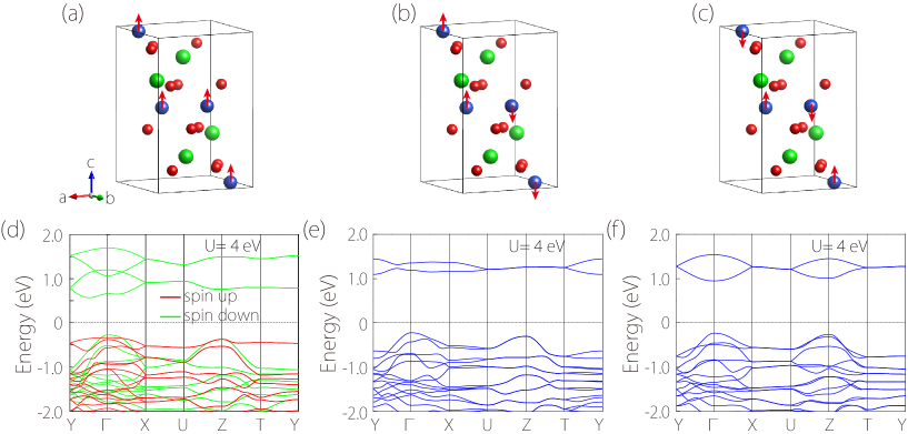
We have assumed the paramagnetic phase for CuTeO3 in this study. Since electrons in Cu may have correlation effects, we have also performed the GGA+ calculations to investigate the possible magnetic phases. We find that for large enough value, a magnetic ground state is preferred. We consider a ferromagnetic (FM) configuration and two antiferromagnetic (AFM) configurations, as illustrated in Fig. 9(a-c). For eV, we find that the AFM configuration in Fig. 9(b) has the lowest energy among the three (each having moment per Cu site). In the band structures, all these magnetic states have a sizable bandgap larger than 1 eV. The FM state still has a nodal loop in the minority spin channel but it is above the Fermi level; whereas the loop is removed in the AFM states. Nevertheless, we note that: (i) Because the electrons are less confined, the Hubbard correction often overestimates the tendency towards magnetism; (ii) No magnetism was observed in experiment at room temperature Pertlik (1987), and although there is no systematic experimental study of this material at lowered temperature, the Neel temperature for closely related compounds such as Cu3TeO6 Li et al. (2017b) and Cu3-xZnxTeO6 Bendaoud et al. (1994) are all below 70 K. Thus, our result presented here should be valid for the temperature range above the material’s Neel temperature, which is not expected to be high.
In conclusion, based on first-principles calculations and symmetry analysis, we predict that the monoclinic CuTeO3 is an almost ideal nodal-loop semimetal. There is a single nodal loop in the band structure close to the Fermi level. The loop is quite flat in energy, and there is no other extraneous band nearby. The drumhead-like surface states corresponding to the nodal surface are identified. We show that the loop is protected by two independent symmetries in the absence of SOC, and the loop can be effectively tuned or even annihilated by strain. When SOC is considered, the nodal loop opens a tiny gap and the system (in a strict sense) becomes a topological metal with spin-polarized surface states. We have constructed a low-energy effective model to describe the nodal-loop phase and the effect of SOC. Since the SOC strength is very small, the monoclinic CuTeO3 is well described as a nodal-loop semimetal. The bulk nodal loop and the surface states can be directly probed in the angle-resolved photoemission (ARPES) experiment. Our result offers a promising platform for exploring the intriguing physics associated with nodal-loop semimetals.
Acknowledgements.
The authors thank X.-L. Sheng, S. Wu, and D. L. Deng for valuable discussions. This work was supported by the National Key RD Program of China (Grant No. 2016YFA0300600), the MOST Project of China (Grant No. 2014CB920903), the NSF of China (Grant No. 11734003 and 11574029), and the Singapore Ministry of Education AcRF Tier 2 (Grant No. MOE2015-T2-2-144). Si Li and Ying Liu contributed equally to this work.Appendix A Band structure result with modified Becke-Johnson potential
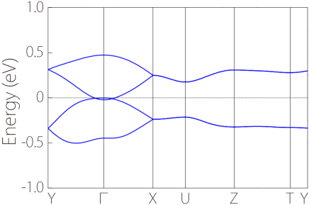
The band structure features are verified by using the more accurate approach with the modified Becke-Johnson (mBJ) potential Tran and Blaha (2009). The result is plotted in Fig. 10. The result indicates that the essential features including the nodal loop remain the same as the GGA result.
References
- Hasan and Kane (2010) M. Z. Hasan and C. L. Kane, Rev. Mod. Phys. 82, 3045 (2010).
- Qi and Zhang (2011) X.-L. Qi and S.-C. Zhang, Rev. Mod. Phys. 83, 1057 (2011).
- Chiu et al. (2016) C.-K. Chiu, J. C. Teo, A. P. Schnyder, and S. Ryu, Rev. Mod. Phys. 88, 035005 (2016).
- Burkov (2016) A. A. Burkov, Nat. Mater. 15, 1145 (2016).
- Armitage et al. (2018) N. Armitage, E. Mele, and A. Vishwanath, Rev. Mod. Phys. 90, 015001 (2018).
- Volovik (2003) G. E. Volovik, The Universe in a Helium Droplet (Clarendon Press, Oxford, 2003).
- Wan et al. (2011) X. Wan, A. M. Turner, A. Vishwanath, and S. Y. Savrasov, Phys. Rev. B 83, 205101 (2011).
- Murakami (2007) S. Murakami, New J. Phys. 9, 356 (2007).
- Burkov and Balents (2011) A. A. Burkov and L. Balents, Phys. Rev. Lett. 107, 127205 (2011).
- Young et al. (2012) S. M. Young, S. Zaheer, J. C. Y. Teo, C. L. Kane, E. J. Mele, and A. M. Rappe, Phys. Rev. Lett. 108, 140405 (2012).
- Wang et al. (2012) Z. Wang, Y. Sun, X.-Q. Chen, C. Franchini, G. Xu, H. Weng, X. Dai, and Z. Fang, Phys. Rev. B 85, 195320 (2012).
- Wang et al. (2013) Z. Wang, H. Weng, Q. Wu, X. Dai, and Z. Fang, Phys. Rev. B 88, 125427 (2013).
- Zhao and Wang (2013) Y. X. Zhao and Z. D. Wang, Phys. Rev. Lett. 110, 240404 (2013).
- Yang and Nagaosa (2014) B.-J. Yang and N. Nagaosa, Nat. Commun. 5, 4898 (2014).
- Weng et al. (2015a) H. Weng, C. Fang, Z. Fang, B. A. Bernevig, and X. Dai, Phys. Rev. X 5, 011029 (2015a).
- Liu et al. (2014) Z. K. Liu, B. Zhou, Y. Zhang, Z. J. Wang, H. M. Weng, D. Prabhakaran, S.-K. Mo, Z. X. Shen, Z. Fang, X. Dai, Z. Hussain, and Y. L. Chen, Science 343, 864 (2014).
- Borisenko et al. (2014) S. Borisenko, Q. Gibson, D. Evtushinsky, V. Zabolotnyy, B. Büchner, and R. J. Cava, Phys. Rev. Lett. 113, 027603 (2014).
- Lv et al. (2015) B. Q. Lv, H. M. Weng, B. B. Fu, X. P. Wang, H. Miao, J. Ma, P. Richard, X. C. Huang, L. X. Zhao, G. F. Chen, Z. Fang, X. Dai, T. Qian, and H. Ding, Phys. Rev. X 5, 031013 (2015).
- Xu et al. (2015a) S.-Y. Xu, I. Belopolski, N. Alidoust, M. Neupane, G. Bian, C. Zhang, R. Sankar, G. Chang, Z. Yuan, C.-C. Lee, S.-M. Huang, H. Zheng, J. Ma, D. S. Sanchez, B. Wang, A. Bansil, F. Chou, P. P. Shibayev, H. Lin, S. Jia, and M. Z. Hasan, Science 349, 613 (2015a).
- Nielsen and Ninomiya (1983) H. B. Nielsen and M. Ninomiya, Phys. Lett. B 130, 389 (1983).
- Son and Spivak (2013) D. T. Son and B. Z. Spivak, Phys. Rev. B 88, 104412 (2013).
- Guan et al. (2017a) S. Guan, Z.-M. Yu, Y. Liu, G.-B. Liu, L. Dong, Y. Lu, Y. Yao, and S. A. Yang, npj Quantum Materials 2, 23 (2017a).
- Mullen et al. (2015) K. Mullen, B. Uchoa, and D. T. Glatzhofer, Phys. Rev. Lett. 115, 026403 (2015).
- Carbotte (2016) J. Carbotte, J. Phys.: Condens. Matter. 29, 045301 (2016).
- Ahn et al. (2017) S. Ahn, E. J. Mele, and H. Min, Phys. Rev. Lett. 119, 147402 (2017).
- Liu et al. (2018) Y. Liu, S. A. Yang, and F. Zhang, Phys. Rev. B 97, 035153 (2018).
- Heikkilä et al. (2011) T. T. Heikkilä, N. B. Kopnin, and G. E. Volovik, JETP Lett. 94, 233 (2011).
- Li et al. (2016) R. Li, H. Ma, X. Cheng, S. Wang, D. Li, Z. Zhang, Y. Li, and X.-Q. Chen, Phys. Rev. Lett. 117, 096401 (2016).
- Chan et al. (2016) Y.-H. Chan, C.-K. Chiu, M. Y. Chou, and A. P. Schnyder, Phys. Rev. B 93, 205132 (2016).
- Wang and Nandkishore (2017) Y. Wang and R. M. Nandkishore, Phys. Rev. B 95, 060506 (2017).
- Liu and Balents (2017) J. Liu and L. Balents, Phys. Rev. B 95, 075426 (2017).
- Rhim and Kim (2015) J.-W. Rhim and Y. B. Kim, Phys. Rev. B 92, 045126 (2015).
- Lim and Moessner (2017) L.-K. Lim and R. Moessner, Phys. Rev. Lett. 118, 016401 (2017).
- Rhim and Kim (2016) J.-W. Rhim and Y. B. Kim, New J. Phys. 18, 043010 (2016).
- Yang et al. (2014) S. A. Yang, H. Pan, and F. Zhang, Phys. Rev. Lett. 113, 046401 (2014).
- Weng et al. (2015b) H. Weng, Y. Liang, Q. Xu, R. Yu, Z. Fang, X. Dai, and Y. Kawazoe, Phys. Rev. B 92, 045108 (2015b).
- Yu et al. (2015) R. Yu, H. Weng, Z. Fang, X. Dai, and X. Hu, Phys. Rev. Lett. 115, 036807 (2015).
- Kim et al. (2015) Y. Kim, B. J. Wieder, C. L. Kane, and A. M. Rappe, Phys. Rev. Lett. 115, 036806 (2015).
- Chen et al. (2015a) Y. Chen, Y. Xie, S. A. Yang, H. Pan, F. Zhang, M. L. Cohen, and S. Zhang, Nano Lett. 15, 6974 (2015a).
- Chen et al. (2015b) Y. Chen, Y.-M. Lu, and H.-Y. Kee, Nat. Commun. 6, 6593 (2015b).
- Fang et al. (2016) C. Fang, H. Weng, X. Dai, and Z. Fang, Chin. Phys. B 25, 117106 (2016).
- Bian et al. (2016) G. Bian, T.-R. Chang, R. Sankar, S.-Y. Xu, H. Zheng, T. Neupert, C.-K. Chiu, S.-M. Huang, G. Chang, I. Belopolski, D. S. Sanchez, M. Neupane, N. Alidoust, C. Liu, B. Wang, C.-C. Lee, H.-T. Jeng, C. Zhang, Z. Yuan, S. Jia, A. Bansil, F. Chou, H. Lin, and M. Z. Hasan, Nat. Commun. 7, 10556 (2016).
- Schoop et al. (2016) L. M. Schoop, M. N. Ali, C. Straßer, A. Topp, A. Varykhalov, D. Marchenko, V. Duppel, S. S. P. Parkin, B. V. Lotsch, and C. R. Ast, Nat. Commun. 7, 11696 (2016).
- Gan et al. (2017) L. Y. Gan, R. Wang, Y. J. Jin, D. B. Ling, J. Z. Zhao, W. P. Xu, J. F. Liu, and H. Xu, Phys. Chem. Chem. Phys. 19, 8210 (2017).
- Li et al. (2017a) S. Li, Z.-M. Yu, Y. Liu, S. Guan, S.-S. Wang, X. Zhang, Y. Yao, and S. A. Yang, Phys. Rev. B 96, 081106 (2017a).
- Zhang et al. (2017) X. Zhang, Z.-M. Yu, X.-L. Sheng, H. Y. Yang, and S. A. Yang, Phys. Rev. B 95, 235116 (2017).
- Huang et al. (2017) H. Huang, K.-H. Jin, and F. Liu, Phys. Rev. B 96, 115106 (2017).
- Jiao et al. (2017) Y. Jiao, F. Ma, C. Zhang, J. Bell, S. Sanvito, and A. Du, Phys. Rev. Lett. 119, 016403 (2017).
- Li et al. (2018) S. Li, Y. Liu, S.-S. Wang, Z.-M. Yu, S. Guan, X.-L. Sheng, Y. Yao, and S. A. Yang, Phys. Rev. B 97, 045131 (2018).
- Xu and Zhang (2016) Y. Xu and C. Zhang, Phys. Rev. A 93, 063606 (2016).
- Gao et al. (2017) Y. Gao, S. A. Yang, and Q. Niu, Phys. Rev. B 95, 165135 (2017).
- Pertlik (1987) F. Pertlik, J. Solid State Chem 71, 291 (1987).
- Kresse and Hafner (1994) G. Kresse and J. Hafner, Phys. Rev. B 49, 14251 (1994).
- Kresse and Furthmüller (1996) G. Kresse and J. Furthmüller, Phys. Rev. B 54, 11169 (1996).
- Blöchl (1994) P. E. Blöchl, Phys. Rev. B 50, 17953 (1994).
- Perdew et al. (1996) J. P. Perdew, K. Burke, and M. Ernzerhof, Phys. Rev. Lett. 77, 3865 (1996).
- Tran and Blaha (2009) F. Tran and P. Blaha, Phys. Rev. Lett. 102, 226401 (2009).
- Anisimov et al. (1991) V. I. Anisimov, J. Zaanen, and O. K. Andersen, Phys. Rev. B 44, 943 (1991).
- Marzari and Vanderbilt (1997) N. Marzari and D. Vanderbilt, Phys. Rev. B 56, 12847 (1997).
- Souza et al. (2001) I. Souza, N. Marzari, and D. Vanderbilt, Phys. Rev. B 65, 035109 (2001).
- (61) M. P. López Sancho, J. M. López Sancho, and J. Rubio, J. Phys. F 14, 1205 (1984); 15, 851 (1985).
- Wu et al. (2017) Q. Wu, S. Zhang, H.-F. Song, M. Troyer, and A. A. Soluyanov, Comput. Phys. Commun. 224, 405 (2017).
- Xu et al. (2015b) Y. Xu, F. Zhang, and C. Zhang, Phys. Rev. Lett. 115, 265304 (2015b).
- Soluyanov et al. (2015) A. A. Soluyanov, D. Gresch, Z. Wang, Q. Wu, M. Troyer, X. Dai, and B. A. Bernevig, Nature 527, 495 (2015).
- Heikkilä and Volovik (2015) T. T. Heikkilä and G. E. Volovik, New J. Phys. 17, 093019 (2015).
- Hyart and Heikkilä (2016) T. Hyart and T. T. Heikkilä, Phys. Rev. B 93, 235147 (2016).
- (67) Y. Gao, Y. Chen, Y. Xie, P.-Y. Chang, M. L. Cohen, and S. Zhang, arXiv:1707.04576 .
- (68) X. Zhang, Z.-M. Yu, Y. Lu, X.-L. Sheng, H. Y. Yang, and S. A. Yang, arXiv:1802.00905 .
- Zhao et al. (2016) Y. X. Zhao, A. P. Schnyder, and Z. D. Wang, Phys. Rev. Lett. 116, 156402 (2016).
- Pan et al. (2014) H. Pan, X. Li, Z. Qiao, C.-C. Liu, Y. Yao, and S. A. Yang, New J. Phys. 16, 123015 (2014).
- Guan et al. (2017b) S. Guan, Y. Liu, Z.-M. Yu, S.-S. Wang, Y. Yao, and S. A. Yang, Phys. Rev. Materials 1, 054003 (2017b).
- Fu and Kane (2007) L. Fu and C. L. Kane, Phys. Rev. B 76, 045302 (2007).
- Fang et al. (2015) C. Fang, Y. Chen, H.-Y. Kee, and L. Fu, Phys. Rev. B 92, 081201 (2015).
- (74) J. Ahn, Y. Kim, and B.-J. Yang, arXiv:1803.11416 .
- Bzdušek et al. (2016) T. Bzdušek, Q. S. Wu, A. Rüegg, M. Sigrist, and A. A. Soluyanov, Nature 538, 75 (2016).
- Wang et al. (2017) S.-S. Wang, Y. Liu, Z.-M. Yu, X.-L. Sheng, and S. A. Yang, Nat. Commun. 8, 1844 (2017).
- Zhong et al. (2016) C. Zhong, Y. Chen, Y. Xie, S. A. Yang, M. L. Cohen, and S. Zhang, Nanoscale 8, 7232 (2016).
- Liang et al. (2016) Q.-F. Liang, J. Zhou, R. Yu, Z. Wang, and H. Weng, Phys. Rev. B 93, 085427 (2016).
- (79) W. Wu, Y. Liu, S. Li, C. Zhong, Z.-M. Yu, X.-L. Sheng, Y. X. Zhao, and S. A. Yang, arXiv:1712.09773 .
- Li et al. (2017b) K. Li, C. Li, J. Hu, Y. Li, and C. Fang, Physical review letters 119, 247202 (2017b).
- Bendaoud et al. (1994) S. Bendaoud, J. Aride, M. Taibi, M. Belaiche, A. Boukhari, and M. Drillon, in Advanced Materials Research, Vol. 1 (Trans Tech , 1994) pp. 553–562.