Tunable electronic properties of partially edge-hydrogenated armchair boron-nitrogen-carbon nanoribbons†
Naresh Alaal,a,b,c Nikhil Medhekar,d and Alok Shuklab,c,‡
Received Xth XXXXXXXXXX 20XX, Accepted Xth XXXXXXXXX 20XX
First published on the web Xth XXXXXXXXXX 200X
DOI: 10.1039/b000000x
We employ first-principles calculations based density-functional-theory (DFT) approach to study electronic properties of partially and fully edge-hydrogenated armchair boron-nitrogen-carbon (BNC) nanoribbons (ABNCNRs), with widths between 0.85 nm to 2.3 nm. Due to the partial passivation of edges, electrons which do not participate in the bonding, form new energy states located near the Fermi-level. Because of these additional bands, some ABNCNRs exhibit metallic behavior, which is quite uncommon in armchair nanoribbons. Our calculations reveal that the metallic behavior is observed for the following passivation patterns: (i) when B atom from one edge, and N atom from another edge, are unpassivated. (ii) when N atoms from both the edges are unpassivated. (iii) when C atom from one edge, and N atom from another edge, are unpassivated. Furthermore, spin-polarization is also observed for certain passivation schemes, which is also quite uncommon for armchair nanoribbons. Thus, our results suggest that ABNCNRs exhibit a wide range of electronic and magnetic properties in that the fully edge-hydrogenated ABNCNRs are direct band gap semiconductors, while partially edge-hydrogenated ones are either semiconducting, or metallic, while simultaneously exhibiting spin polarization, based on the nature of passivation. We also find that the ribbons with larger widths are more stable, as compared to the narrower ones.
1 Introduction
Successful synthesis of graphene1 has led to intensive research activities aimed at the discovery of novel nanomaterials. Low-dimensional materials have distinctive electronic properties when compared to their bulk counterparts, because of the effects of quantum confinement2, 3. Several other two-dimensional (2D) materials such as h-BN monolayer, transition metal dichalcogenides, phosphorene, and borophene have been successfully synthesized over the years4, 5, 6, 7. Graphene has received remarkable attention from the researchers due to its unusual properties such as high carrier mobility at room temperature, high electrical conductivity, high thermal conductivity, and excellent mechanical strength8, 9, 10, 11. Although graphene exhibits many interesting properties, but its applications are limited as far as electronic devices are concerned, due to its zero band gap. Thus, graphene cannot be used in those devices, which require switching between states of low and high conductivity8, 1. Several techniques have been discovered, which can open up a band gap in graphene, such as: (a) the use of suitable substrates, (b) patterning into one-dimensional (1D) nanoribbons, (c) strain engineering, (d) chemical functionalization, and (e) doping with isoelectronic atoms12, 13, 14, 15, 16, 17, 18, 19, 20, 21.
Another promising technique that introduces a band gap in graphene is by forming graphene and h-BN composites. Boron-nitrogen-carbon (BNC) monolayer synthesized by Li et al.22, opened the possibility of combining graphene and 2D h-BN domains, because: (a) C-C bond length 1.42 Å is very close to B-N bond length 1.44 Å, and (b) C-C and B-N units are isoelectronic. These monolayers have completely distinct properties from their parent materials, graphene, and 2D h-BN monolayer. Experimental synthesis of 2D BNC monolayer led to a large number of theoretical, as well as experimental, studies of graphene-BN composites consisting of CC and BN units in various proportions.23, 24, 25, 26, 27, 28, 29
Nanoribbons, which are obtained by truncating 2D materials into 1D ones, also exhibit interesting electronic, magnetic and optical properties on the basis of their width, and decoration of edges30, 31. Graphene nanoribbons (GNRs) and boron nitride nanoribbons (BNNRs) have been experimentally fabricated by unwrapping of carbon nanotubes and BN nanotubes, respectively32, 33. Armchair GNRs (AGNRs) are non-magnetic semiconductors for all widths, have oscillating band gaps over families, and approach the value of a 2D sheet for large widths34. Zigzag GNRs (ZGNRs) have tunable band gaps from metal to semiconductor depending on the width and passivation of edges35, 36. It has also been demonstrated theoretically that ZGNRs exhibit half-metallic behavior when electric field is applied across their width37. ABNNRs are non-magnetic semiconductors, for which the band gap decreases with increasing width of the nanoribbon. ZBNNRs are either magnetic, or nonmagnetic, depending on their edge passivation38, 39, 40.
Similarly, BNC nanoribbons (BNCNRs), if synthesized, can also contain boron, nitrogen, and carbon atoms in various proportions. Although BNC nanoribbons have not been experimentally realized yet, they have been studied extensively using various theoretical methods.41, 42, 43, 44, 45, 46, 47, 38, 48, 49, 50, 51, 52, 53, 54. Huang et al.45 studied the hybrid bare BNC nanoribbons obtained by combining BNNRs and GNRs, by using first-principles DFT approach. They found that armchair BNC nanoribbons (ABNCNRs) are non-magnetic semiconductors, while zigzag BNC nanoribbons (ZBNCNRs) exhibit half-metallicity for certain widths, and C/BN compositions. Liu et al.46 studied the electronic structures of hybrid ABNCNRs by using the DFT approach. They found that these nanoribbons are magnetic metals when the B and N atoms are unpaired, and that they also exhibit half-metallic behavior when the O atoms are adsorbed on appropriate positions of nanoribbons. Kan et al.43 studied spin-polarized electronic properties of fully hydrogen-passivated zigzag BNC nanoribbons by using first-principles DFT, and reported that due to a competition between charge and spin polarization, these nanoribbons can exhibit half-metallic behavior. Fan et al.52 studied unpassivated ZBNCNR structures obtained by joining ZGNRs and ZBNNRs along the width, and they found that the electronic properties can be tuned by changing the width of the ZGNR domain. Dihydrogenated ZBNCNRs were studied by Liu et al. 44, and they reported that the half-metallic property depends on the width of both the carbon, and the BN domains. Basheer et al.38 studied fully hydrogen-passivated, and partially passivated ZBNCNRs, which are composed of an equal number of C, B and N atoms. They observed that the half-metallic behavior depends on the edge passivating atoms, and the width of the ribbon.
Generally, edge passivation plays a key role in modifying electronic structures of nanoribbons 55, 56, 57, 58, 59. Interestingly, partial edge passivation also leads to interesting electronic properties in nanoribbons60, 61. For example, ABNNRs were found to be half-metallic when edge B atoms are passivated, and edge N atoms are left unpassivated61. Similarly, zigzag SiC naniribbons behave as magnetic metals when edge Si atoms are unpassivated, while they become magnetic semiconductors, when edge C atoms are unpassivated60. Although one study of partially passivated ZBNCNRs exists38, to the best of our knowledge, no such studies of ABNCNRs have been undertaken.
In this work, we present a detailed study of electronic properties of ABNCNRs, whose edges are fully and partially passivated with hydrogen atoms. Our calculations suggest that by partial edge passivation, one can tune electronic properties of ABNCNRs in a variety of ways such as non-magnetic semiconductors, magnetic semiconductors, or magnetic metals, depending on the nature of edges, and their passivation. This is an interesting result because normally no magnetic behavior is expected in case of armchair nanoribbons. We also found that few configurations of ABNCNRs exhibit metallic behavior irrespective of their widths, and ribbons with larger width are more stable as compared to the narrower ones.
Remainder of the paper is organized as follows. In the next section we describe our theoretical methodology, in section III we present and discuss our results, while in section IV we summarize and conclude.
2 Computational Details
Computational methodology followed in this work is similar to the one adopted in our previous works on SiCNRs,58, 59 except that the present calculations are limited to the level of density-functional theory (DFT). We performed all the calculations using the software package VASP62, in which the ground state properties are computed using a plane-wave based first-principles, DFT approach. We chose to adopt the generalized-gradient approximation (GGA) approach for the exchange correlation functional, coupled with Perdew, Burke, Enzerhof (PBE) pseudopotentials.63, 64 A kinetic energy cut-off of 500 eV was used, along with a k-point grid of , employed for structural relaxation. Convergence threshold energy of eV was used, and atoms were relaxed until the force on each atom was less than eV/Å. After the geometry optimization, charge density profiles were computed using a superior k-point mesh of . Nanoribbons studied here are considered periodic in the direction, and vacuum (intercell distance) of more than 14 Å has been taken in and directions to model this 1D structure. The widths of ABNCNRs are represented by the integer , which equal to the total number of C-C/BN pairs across the width. In this work we present our calculations on ABNCNRs with widths ranging between 0.85 nm to 2.3 nm, corresponding to ribbons with .
3 Results And Discussion
3.1 Band Structures of Graphene and Boro-Nitride Nanoribbons
Before considering the cases of partially saturated ABNCNRs, we compute the band structures of armchair type graphene nanoribbons (AGNRs), and boron nitride nanoribbons (ABNNRs).
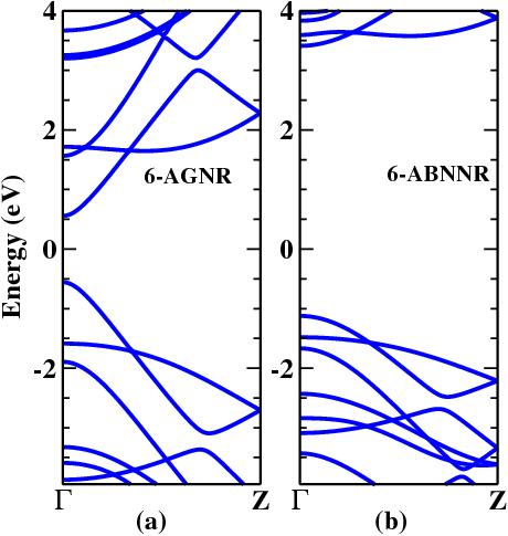
Because ABNCNRs of a given width are combinations of AGNRs and ABNNRs, therefore, in order to achieve a deeper understanding of their electronic structure, it will be helpful to know the band structures of the original, unmixed nanoribbons. In particular, we compute the band structures of 6-AGNR and 6-ABNNR, and in both the cases we assume that the edge atoms are saturated by hydrogens. The calculated band structures of these ribbons, along the line connecting high symmetry Brillioun zone points, and X, are presented in Fig. 1. As is obvious from the figure that for both the ribbons, the valence band maximum (VBM), and the conduction band minimum (CBM) occur at high symmetry Brillioun zone point , implying that these are direct band gap materials. The calculated band gaps of 1.11 eV (6-AGNR) and 4.53 eV (6-ABNNR) are in good agreement with the results reported by other authors65, 66. This establishes the accuracy of the computational methodology employed by us, which we utilize in the following sections to study the electronic structure of various configurations of ABNCNRs.

3.2 Nature of Bonds and Stability of ABNCNRs
Henceforth we consider ABNCNRs, which consist of an equal number of C-C and B-N dimers, along the width. We use the notation x-y-ABNCNR to denote a given nanoribbon, in which x and y denote the dimer units terminating the two edges. Thus, based upon their edge terminations, nanoribbons are divided into three configurations labeled as BN-BN-ABNCNR, CC-CC-ABNCNR, and CC-BN-ABNCNRs. In BN-BN-, and CC-CC-ABNCNRs, both the edges are composed only of BN and CC dimer units, respectively. In the CC-BN configuration, one edge is composed of CC dimers, while the other one is composed of BN dimers. Geometrical structures of ABNCNRs are presented in Fig. 2. From previous studies22, 67, 38, 2D BNC nanostructures which consist of maximum number of B-N and C-C bonds, are more stable as compared to any other structures, which have other types of bonds (say, B-C, N-C, B-B and N-N, bonds). Here we quantitatively examine the stability of various configurations of ABNCNRs, as a function of the number of bonds of various types present in the nanoribbon, and present the results in Table 1. All the nanoribbons considered are assumed to have hydrogen passivated edges. We do not consider structures with B-B and N-N bonds in our study, because they are even more unstable38, 68.
| Structure | No. of | No. of | No. of | No. of | Relative |
|---|---|---|---|---|---|
| B-N bonds | C-C bonds | B-C bonds | N-C bonds | energy (eV) | |
| 6-BN-BN-ABNCNR | 6 | 3 | 2 | 2 | 1.38 |
| 6-CC-CC-ABNCNR | 5 | 4 | 2 | 2 | 0.63 |
| 6-CC-BN-ABNCNR | 6 | 5 | 1 | 1 | 0 |
From Fig. 2 and Table 1, 6-CC-BN-ABNCNR consists of maximum number of C-C (5) and B-N (6) bonds, and it is clear that the total energies of 6-BN-BN-ABNCNR and 6-CC-CC-ABNCNR are 1.38 eV and 0.63 eV, respectively, higher than that of 6-CC-BN-ABNCNR. Total energies per unit cell of these nanoribbons are in following order: CC-BN-ABNCNR<CC-CC-ABNCNR<BN-BN-ABNCNR. Thus, CC-BN-ABNCNR corresponds to the most stable configuration, when compared with the other two types of ABNCNRs. We conclude that these nanoribbons become more unstable with the increasing number of B-C and N-C bonds, and with the decreasing numbers of C-C and B-N bonds.
3.3 Electronic properties of BN-BN-ABNCNRS

BN-BN-ABNCNRs are divided into eight configurations based on how the edge atoms are passivated with the hydrogen atoms. These configurations can be described as: (a) both the upper and lower edge atoms are passivated with hydrogen, (b) the upper edge atoms are passivated with H, and lower edge atoms are unpassivated, (c) lower edge atoms are passivated with H, and upper edge atoms are unpassivated, (d) N atoms from both the edges are terminated with H, while B atoms from both the edges are unpassivated, (e) B atoms from both the edges are terminated with H, while N atoms from both the edges are unpassivated, (f) B atoms on the upper edges and N atoms on the lower edge lower are passivated with H, while remaining edge atoms are unpassivated, (g) N atoms on the upper edge and B atoms on the lower edge are passivated with H, while remaining edge atoms are unpassivated. (h) Both the edges are unpassivated. These configurations are labeled as: BHNH-BHNH-ABNCNR (a0), BHNH-BN-ABNCNR (a1), BN-BHNH-ABNCNR (a2), BNH-BNH-ABNCNR (a3), BHN-BNH-ABNCNR (a4), BNH-BHN-ABNCNR (a5), BHN-BHN-ABNCNR (a6), BN-BN-ABNCNR (a7). Thus, in this notation, superscript H on an edge atom indicates its passivation by hydrogen. Fig. 3 displays the geometric structures and lattice parameters of these eight configurations of BN-BN-ABNCNRs, corresponding to various edge-passivation schemes. Configuration a0, and a7, represent fully hydrogen-passivated, and bare BN-BN-ABNCNRs, respectively. These ABNCNRs have different lattice constants ranging from 4.32 to 4.35 Å.
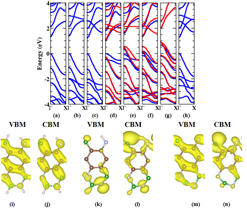
Band structures for all the BN-BN-ABNCNRs configurations are presented in Fig. 4, while Table 2 presents the band gaps, magnetic moments, energy difference ) between magnetic and nonmagnetic states, and the values of Gibbs free energy of formation () for all the configurations of BN-BN-ABNCNRs. All the band structures are plotted along the line joining high symmetry Brillioun zone points and , while the Fermi-level has been set to 0 eV. Fig. 4 shows that configurations a0, a1, a2, and a7 are direct band gap semiconductors because VBM and CBM for these structures occur at same high Brillioun zone point . In Figs. 4 (d)-(g), blue lines and red lines represent band structures for spin-up and spin-down channels, respectively. Thus, it is obvious that configurations a3, a4, a5, and a6 exhibit spin-polarized behavior, which would not have been possible for fully hydrogen-passivated ABNCNRs. Furthermore, from Table 2 it is clear that, configuration a3 is a magnetic semiconductor because band gaps for up and down spins are unequal, and in the semiconducting range. Examination of Fig. 4 and Table 2 further reveals that configurations a4, a5, and a6 are magnetic metals because: (a) their bands are spin-polarized, (b) valence and conduction bands for both spin orientations cross the Fermi-level, and (c) they have finite magnetic moment per unit cell. Thus, in partially edge-hydrogenated BN-BN-ABNCNRs, spin-polarization is observed only when one atom from the upper edge, and another one from the lower edge, are unpassivated. In particular, metallic behavior appears when: (a) B atom from one edge, and N atom from another one, are passivated, or (b) when N atoms from both the edges are unpassivated.
| Configuration | Band gap (eV) | () | Type | (eV) | (eV) | (eV/Å) | (eV) | |
| Up | Down | |||||||
| a0 | 1.34 | 1.34 | 0 | NM | - | 0.180 | 0.332 | -4.803 |
| a1 | 1.40 | 1.40 | 0 | NM | - | 0.411 | 0.660 | -4.821 |
| a2 | 1.24 | 1.24 | 0 | NM | - | 0.413 | 0.669 | -4.803 |
| a3 | 1.04 | 1.37 | 0.98 | FM | 0.894 | 0.536 | 0.868 | -3.944 |
| a4 | M | M | 0.92 | FM | 0.519 | 0.539 | 0.873 | -3.922 |
| a5 | M | M | 0.01 | Ferri | 0.314 | 0.554 | 0.898 | -3.814 |
| a6 | M | M | 0.12 | Ferri | 0.004 | 0.550 | 0.891 | -3.845 |
| a7 | 1.30 | 1.30 | 0 | NM | - | 0.724 | 0.999 | - |
To understand the atomic contributions to the magnetic moment of the unit cell, we have performed calculations for the supercells containing double units and presented spin density plots of the four configurations (a3-a6) in Fig. 5. For the configurations a3-a4, we note that the magnetic moments are predominantly due to the spin-up states, derived mainly from the unpassivated edge atoms, and have large magnetic moments with ferromagnetic behavior. In case of a5 and a6, we find that the magnetic moments are too small when compared with other spin-polarized configurations (see Table 2), because spins on the two edges are almost equal in magnitude, and oppositely oriented, resulting in a small net magnetic moment. Thus, both these configurations are ferrimagnetic metals. The energy difference between the magnetic and nonmagnetic states tells that a3 is the most stable magnetic configuration, and a6 is the least stable one. Thus, we conclude that partially passivated BN-BN ABNCNRs can be non-magnetic semiconductors, magnetic semiconductors, or magnetic metals, depending upon the nature of edge passivation by H atoms.
We also calculated the partial charge density profiles in order to understand the contribution of various atoms to the valence band maxima (VBM) and the conduction band minima (CBM) of BN-BN-ABNCNRs, and in Figs. 4 (i)–(m) we present those for configurations , , and a7. We observe that, in configuration , the VBM and CBM derive their dominant contribution from the C-C pairs, with upper edge atoms also contributing significantly. In the partially passivated a5 configuration, the VBM and CBM are mainly localized on unpassivated atoms. In configuration a7, we can observe that the edge atoms undergo reconstruction, and that the VBM is mainly composed of contributions from C-C pairs, while the CBM is localized on the unpassivated upper edge atoms.
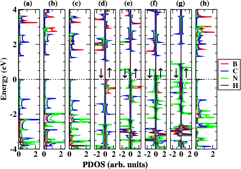
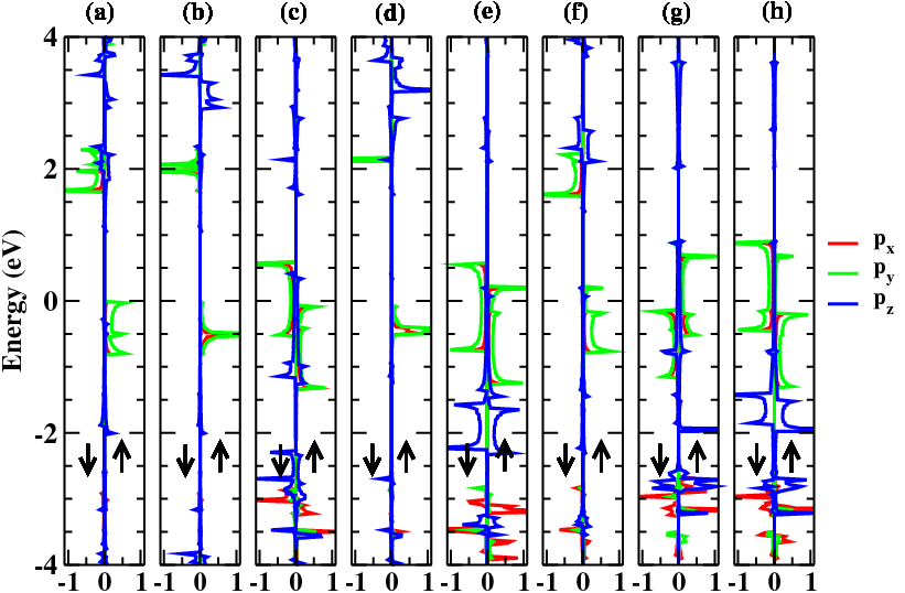
In order to understand the origins of changes in the band structures of these nanoribbons, with various edge hydrogenation patterns, we present projected density of states (PDOS) for individual atoms in the Fig. 6. We also present PDOS corresponding to the orbitals of the bare edge atoms of spin-polarized configurations in the Fig. 7. We find that in the nonmagnetic BN-BN-ABNCNRs (a0, a1, a2 and a7), VBM and CBM originate mainly from the C atoms, with small contribution from N atoms. In all the configurations, H atoms contribute to the states which are away from the Fermi level in the valence band. In the spin-up channel of configuration a3, VBM originates mainly from the B atoms, and particularly from py orbital of upper edge B atom, while CBM is derived from C atoms (See Fig. 6 (d) and Figs.7(a)-(b)). In the spin-down channel, VBM and CBM both originate from C atoms. In the spin-up and spin-down channels of configurations of a4-a6, VBMs cross Fermi-level, because of the additional energy states that are mainly contributed by the orbitals of the N atoms (See Figs. 6 (e)-(g) and Figs. (c)-(h)), causing them to become metallic.
We also performed Bader charge analysis 69 for various nanoribbons, and in Table 3 we present the computed Bader charges on the edge atoms of the spin-polarized BN-BN configurations a3-a6 , and compare them with the charges on edge atoms of the bare BN-BN-ABNCNR (configuration a7). From the table we observe that in the configurations a3-a5, bare edge atoms accumulate the electrons, while the hydrogenated ones lose them. For example, in case of a3, the left upper edge (LUE) atom (B) and left lower edge (LLE) (B) atom gain the charge of 0.46 and 0.41 respectively. On the other hand, right upper edge (RUE) atom (N) and right lower edge (RLE) atom (N) lose the charges of 0.24 , and 0.06 , respectively. In configuration a6, one bare edge accumulates the electronic charge, while the other one loses it. One common feature is when hydrogen atoms passivate the boron atoms (H on LUE and H on LLE) they show high electronegativity, as compared with nitrogens passivated by hydrogen atoms (H on RUE and H on RLE).

| Configuration | LUE (B) | RUE(N) | LLE (B) | RLE (N) | H-LUE | H-RUE | H-LLE | H-RLE |
| a3 | 1.87 (+0.46) | 6.17(-0.24) | 1.75 (+0.41) | 6.63(-0.06) | - | 0.676 | - | 0.619 |
| a4 | 1.40(-0.01) | 6.11(+0.30) | 1.71(+0.37) | 6.62(-0.07) | 1.585 | - | - | 0.680 |
| a5 | 1.83(+0.42) | 6.21(-0.20) | 0.90(-0.44) | 6.76(+0.07) | - | 0.683 | 1.639 | - |
| a6 | 1.43(+0.02) | 6.01(-0.40) | 0.91(-0.43) | 6.76(+0.07) | 1.537 | - | 1.636 | - |
| a7 | 1.41 | 6.41 | 1.34 | 6.69 | - | - | - | - |
3.4 Electronic properties of CC-CC-ABNCNRS

CC-CC-ABNCNRs are also divided into eight configurations based on how their edge atoms are passivated with hydrogen atoms. Similar to BN-BN BNCNRs, CC-CC-ABNCNRs are also divided into eight configurations, based on their edge passivation patterns, as presented in Fig. 8: CHCH-CHCH-ABNCNR (b0), CHCH-CC-ABNCNR (b1), CC-CHCH-ABNCNR (b2), CCH-CCH-ABNCNR (b3), CHC-CCH-ABNCNR (b4), CCH-CHC-ABNCNR (b5), CHC-CHC-ABNCNR (b6), CC-CC-ABNCNR (b7). As is obvious from Fig. 8, configurations b0and b7 represent fully hydrogen-passivated, and completely bare CC-CC-ABNCNRs, respectively. These ABNCNRs have lattice constants in the range 4.35 to 4.41 Å (See Fig. 8).
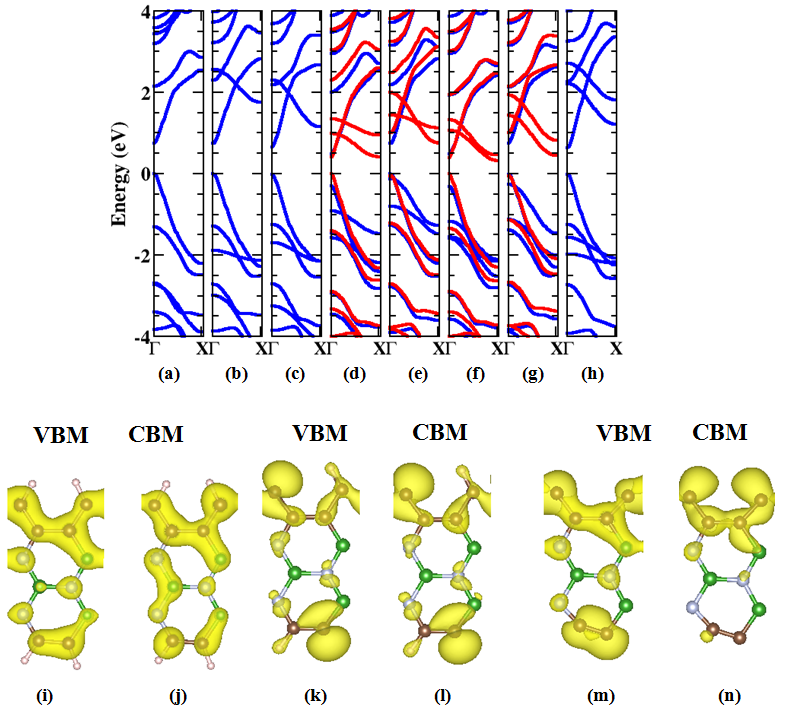
In Fig. 9 we present the band structures of all the configurations of CC-CC-ABNCNRs, while Table 4 contains corresponding band gaps, magnetic moments, and cohesive energies. From Figs. 9 (a)-(c), and (h) it is obvious that the nanoribbons with configurations b0, b1, b2, and b7, are all direct band gap semiconductors. Band structures of configurations b3, b4, b5, and b6 presented in Figs.9 (d)-(g), and band gaps and magnetic moments presented in Table 4, make it obvious that these nanoribbons exhibit spin-polarized behavior, with different band gaps for the two spin orientations, both of which are in the semiconducting range. Thus, we conclude that CC-CC-ABNCNRs configurations are either magnetic, or non-magnetic semiconductors, but never metallic.
| Configuration | Band gap (eV) | () | Type | (eV) | (eV) | (eV/Å) | (eV) | |
| Up | Down | |||||||
| b0 | 0.75 | 0.75 | 0 | NM | - | 0.133 | 0.244 | -5.255 |
| b1 | 0.74 | 0.74 | 0 | NM | - | 0.417 | 0.667 | -5.305 |
| b2 | 0.65 | 0.65 | 0 | NM | - | 0.429 | 0.683 | -5.215 |
| b3 | 0.78 | 0.40 | 0 | AFM | 0.687 | 0.517 | 0.832 | -4.601 |
| b4 | 0.75 | 0.74 | 0 | AFM | 0.074 | 0.504 | 0.809 | -4.694 |
| b5 | 0.63 | 0.32 | 0 | AFM | 0.054 | 0.530 | 0.851 | -4.513 |
| b6 | 0.79 | 0.41 | 0 | AFM | 0.105 | 0.515 | 0.828 | -4.614 |
| b7 | 0.64 | 0.64 | 0 | NM | - | 0.812 | 1.105 | - |
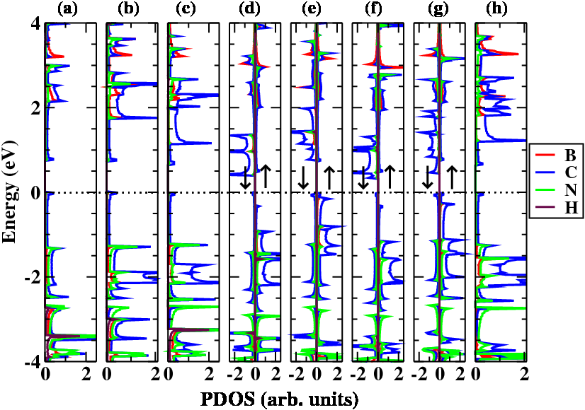
In Figs. 9 (i) and (j), (k) and (l), (m) and (n), we present partial charge density profiles for configurations b0, b5, and b7, respectively. We note that: (a) the VBM and CBM of configuration b0 are derived mainly from carbon atoms, (b) for b5 both the VBM and CBM originate from the bare-edge atoms, with similar charge distributions, and (c) in configuration b7, the VBM derives its contributions from both the edges, while the CBM is localized on the upper edge unpassivated C atoms. Similar to BN-BN-ABNCNRs, CC-CC-ABNCNRs also exhibit spin polarization when one atom from the upper edge, and another atom from the lower edge, are unpassivated. However, unlike BN-BN-ABNCNRs, no metallic behavior is observed in partially edge-hydrogenated CC-CC-ABNCNRs. PDOS of various configurations of 6-CC-CC-ABNCNR is presented in Fig.11. From, the Fig. 11, it is clear that for both the nonmagnetic and the magnetic configurations, VBM and CBM derive their main contributions from the C atoms. In the spin-down channels of configurations b3-b6, the CBMs are mainly derived from the py orbitals of the unpassivated edge C atoms (Fig.1 of Supporting Information). In Fig. 10 we present the spin-density plots of configurations b3-b6. From the Fig. 10 and Table 4, it is clear that the spin-polarized configurations exhibit antiferromagnetic alignment with zero net magnetic moments, because of equal number of spin-up and spin-down states. It is also obvious from energetic considerations that configuration b3 is the most stable magnetic configuration among all the magnetic configurations of BN-BN-ABNCNRs (See Table 4).

Table 5 presents the Bader charges on the edge atoms of configurations b3 to b6 and compared with b7. Except in the configuration b5, one hydrogen-passivated edge atom loses the electrons and another one gains the electrons in configurations b3, b4 and b6. Since all the edge atoms are carbons, we did not find any significant difference in the charges of hydrogen atoms.
| Configuration | LUE (C) | RUE(C) | LLE (C) | RLE (C) | H-LUE | H-RUE | H-LLE | H-RLE |
| b3 | 3.89(-0.24) | 4.18(-0.05) | 3.39(-0.18) | 4.95(+0.20) | - | 0.930 | - | 0.910 |
| b4 | 4.06(-0.07) | 4.27(+0.04) | 3.40(-0.17) | 4.95(+0.20) | 0.979 | - | - | 0.921 |
| b5 | 4.00(-0.13) | 4.11(-0.12) | 3.80(+0.23) | 4.53(-0.22) | - | 0.998 | - | 0.954 |
| b6 | 4.11(-0.02) | 4.18(-0.05) | 3.87(+0.30) | 4.52(-0.23) | 0.950 | - | 0.975 | - |
| b7 | 4.13 | 4.23 | 3.57 | 4.75 | - | - | - | - |
3.5 Electronic properties of CC-BN-BNCNRS

Like previously discussed ribbons, CC-BN-ABNCNRs are also divided into eight configurations based on the edge atom passivation scheme: CHCH-BHNH-ABNCNR (c0), CHCH-BN-ABNCNR (c1), CC-BHNH-ABNCNR (c2), CCH-BNH-ABNCNR (c3), CHC-BNH-ABNCNR (c4), CCH-BHN-ABNCNR (c5), CHC-BHN-ABNCNR (c6), CC-BN-ABNCNR (c7). All the geometrical structures of partially hydrogen-passivated CC-BN-ABNCNRs are presented in Fig. 12, from which it is clear that configurations c0 and c7 represent fully hydrogen-passivated, and bare CC-BN ABNCNRs, respectively. These ABNCNRs have lattice constants in the range 4.34 to 4.39 Å (See Fig. 12).
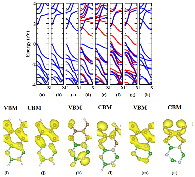
Electronic structures of various CC-BN-ABNCNRs configurations are presented in Fig. 13, while Table 6 contains their band gaps, magnetic moments, and cohesive energies. Figs. 13 (a)-(c) and (h) display band structures for configurations c0, c1, c2, and c7, making it obvious that they are all non-magnetic semiconductors, out of which c0 and c1 have direct band gaps. We note that configurations c2 and c7 have indirect band gaps, while in comparison, for BN-BN-, and CC-CC-ABNCNRs, band gaps of all non-magnetic semiconductors are direct in nature. From Figs. 13 (d)-(g), and Table 6, based upon split bands, and different band gaps for the two spin orientations, we conclude that the nanoribbons with configurations c3-c6, exhibit spin-polarized behavior. In configurations and , both the band gaps have semiconducting behavior, while in configurations c5 and c6 the valence and the conduction bands cross Fermi-level, thereby rendering them metallic. But, the metallicity in c5 and c6 is magnetic in nature because of the spin-polarized character of their band structure, and finite magnetic moments. Therefore, similar to the case of BN-BN-ABNCNRs, we can also tune CC-BN-ABNCNRs into semiconductors, magnetic semiconductors, or magnetic metals by manipulating scheme of partial edge passivation.
| Configuration | Band gap (eV) | () | Type | (eV) | (eV) | (eV/Å) | (eV) | |
| Up | Down | |||||||
| c0 | 1.85 | 1.85 | 0 | NM | - | 0.093 | 0.172 | -5.075 |
| c1 | 1.86 | 1.86 | 0 | NM | - | 0.307 | 0.493 | -5.400 |
| c2 | 1.32 | 1.32 | 0 | NM | - | 0.398 | 0.490 | -4.908 |
| c3 | 1.37 | 1.10 | 1.08 | FM | 0.674 | 0.459 | 0.740 | -4.484 |
| c4 | 1.34 | 1.18 | 0 | AFM | 0.197 | 0.456 | 0.735 | -4.503 |
| c5 | M | M | 1.23 | FM | 0.321 | 0.496 | 0.800 | -4.222 |
| c6 | M | M | 0 | AFM | 0.357 | 0.494 | 0.798 | -4.232 |
| c7 | 1.49 | 1.49 | 0 | NM | - | 0.699 | 0.956 | - |
Figs. 13 (i) and (j), (k) and (l), and (m) and (n) present partial charge density profiles for configurations c0, c5,and c7, respectively. The VBM and CBM of c0 have dominant presence mainly on carbon atoms, with similar charge distributions. In c5, the VBM has dominant presence on the lower BN edge, while CBM originates mainly from the upper edge C atoms (see Figs. 13 (k) and (l)). In case of configuration c7, the charge density corresponding to the VBM is delocalized significantly over the entire width, while for the CBM it is mainly localized on upper edge carbon atoms.
We note that for CC-BN-ABNCNRs, metallic behavior is observed only when C atom from one edge, and N atom from another edge are left bare. As far as spin polarization is concerned, similar to the other two classes of ABNCNRs previously discussed, these nanoribbons exhibit it only when one atom on each edge is passivated.
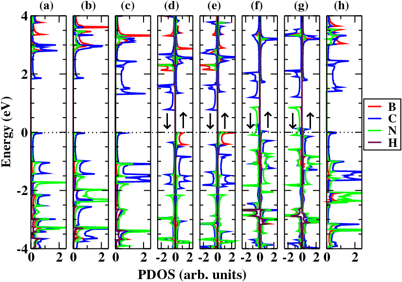
Fig.14 presents PDOS of all the configurations of 6-CC-BN-ABNCNR. Similar to the BN-BN-ABNCNRS, VBM and CBM of nonmagnetic CC-BN-ABNCNR configurations are derived from the C atoms. In the spin-up channel configurations of c3 and c4, VBMs are mainly contributed by B atoms, with small contributions also from the N atoms. In the spin-down channel, CBMs are derived essentially from the C atoms. In the c5 and c6 configurations, additional bands arise due to the following contributions: (a) VBMs originate from the C atoms in the spin-up channel, and (b) N atoms contribute to the VBM in the spin-down channel. These additional energy bands around the Fermi level turn them into metals. We also present PDOS of orbitals of the bare edge atoms of spin-polarized configurations (c3-c6) in Fig. 3 of the Supporting Information. It is obvious that the metallic behavior in c5 and c6 configurations is originating from the anti-bonding electrons of py orbitals. Spin density plots of configurations c3-c6 are presented in the Fig. 15. From Table 6 and Fig. 15 it is clear that the electrons from the unpassivated edge atoms contribute to the magnetic moments, with c3 and c5 exhibiting ferromagnetic behavior, and c4 and c6 showing antiferromagnetic alignment. Energetically speaking, the most stable configuration among all the magnetic configurations of CC-BN-ABNCNRs is c3.

Bader charges on the edge atoms after the partial passivation are presented in the table 7 for configurations c3-c6, and are compared with those on the bare CC-BN configuration (c7). In configuration c3, except RUE, all other edge atoms gain electronic charge. In configurations c5 and c6, both LUE and LLE atoms gain electrons. Interestingly, in the configuration c4 two edge atoms gain the electronic charge, while another two lose it. In configurations c3 and c4, N atoms passivated by H atoms have low charges, while in the configuration c5 and c6, H-RLE and H-LLE are found to have high electronic charges.
| Configuration | LUE (C) | RUE(C) | LLE (B) | RLE (N) | H-LUE | H-RUE | H-LLE | H-RLE |
| c3 | 4.20(+0.15) | 3.94 (-0.23) | 1.60 (+0.37) | 6.74 (+0.19) | - | 0.976 | - | 0.625 |
| c4 | 3.94(-0.11) | 4.15(-0.02) | 1.61(+0.38) | 6.72(+0.17) | 0.971 | - | - | 0.629 |
| c5 | 4.27(+0.22) | 3.93(-0.24) | 1.22(-0.01) | 6.39(-0.16) | - | 0.973 | - | 1.601 |
| c6 | 4.01(-0.04) | 3.98(-0.09) | 1.27(+0.04) | 6.35(-0.20) | 0.946 | - | 1.600 | - |
| c7 | 4.05 | 4.17 | 1.23 | 6.55 | - | - | - | - |
3.6 Relative Stability of ABNCNRs
In this section we discuss the relative stability of various configurations of ABNCNRs, based upon their zero temperature Gibbs free energies of formation (G) presented in the Tables 2, 4, and 6. was computed using the following formula which has been used by other authors for structures with a variety of chemical compositions70, 43, 71, 72.
where , , , and are the chemical potentials of atoms C, B, H, and N, respectively; , , , and are the molar fractions of C, B, H, and N atoms, respectively, satisfying the rule , and is defined as the cohesive energy per atom in the infinite monolayer graphene sheet. We can write the equation above as
where is the cohesive energy per atom of the ribbon in question; denotes the chemical potential of the BN dimer calculated as cohesive energy per unit cell of the 2D monolayer of BN, and represents the molar fraction of BN units. is computed as the binding energy per atom of H2 molecule43, and to account for the thermodynamic equilibrium of and , we used the constraint : .68, 53 Cohesive energy per atom of the ribbon is defined as
above , , , and are the total energies of isolated atoms C, B, H, and N, respectively; , , , and are the numbers of C, B, H, and N atoms, respectively, in the unit cell, while , is the total number of atoms per cell.
Generally a lower Gibbs free energy of formation implies a higher stability of the system. As we have already discussed in earlier sections that fully edge-hydrogenated ABNCNRs (a0, b0, and c0) have the relative stability in the order c0 b0 a0, while bare ABNCNRs exhibit the order c7 a7 b7.
We also compared partially edge-hydrogenated ABNCNRs, and found that within a class of nanoribbons, the following stability order is observed: (i) a1 a2 a3 a4 a6 a5, (ii) b1 b2 b4 b6 b3 b5, and (iii) c1 c2 c4 c3 c6 c5. The common feature among these orders is that the most stable of the partially passivated ribbons in a given class is the ribbon whose both upper edge atoms are saturated. The least stable configurations also have a common feature in that one upper, and another lower edge atom are saturated, which are diagonally across, and topologically similar, across the three classes of nanoribbons (see Figs. 3, 8, and 12).
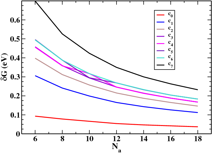
We also present the behavior of the Gibbs free energies of the most stable configurations of CC-BN-ABNCNRs, as a function of their width in the Fig. 16. We find that the Gibbs free energies of all the configurations decrease with the increasing width, implying that the ribbons with larger widths are more stable compared to the narrower ones, similar to ABNNRs40.
We also calculated edge formation energy per unit length ()58 of ABNCNRs by using the formula
where is the total energy/cell of the nanoribbon, is the energy per BN dimer of BN sheet, is the total energy of H2 molecule, is the total number of BN dimers, and L is the length of the edge (in Å ) of the given nanoribbon. The binding energy per H atom ()51 for the given ribbon was computed as
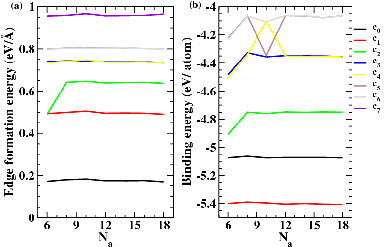
where H-ABNCNR is the total energy of partially or fully hydrogenated ABNCNR and is the total energy of the corresponding bare ABNCNR. and are presented in Tables 2, 4, and 6 for Na=6, for various ABNCNRs. For all the configurations of CC-BN-ABNCNRs, we have presented the width dependence of and in Figs. 17 (a) and (b), respectively. From the tables (See Tables 2, 4, and 6), it is clear that exhibits similar trends as for Na=6, implying that the fully hydorgenated ABNCNRs are more favorable towards edge formation than the ones which are partially passivated, or completely bare. Considering the values for Na=6 (See Tables 2, 4, and 6), we found that the fully and the partially edge hydrogenated ABNCNRs have negative binding energies in the range of -5.40 eV/atom to -3.81 eV/atom. This indicates that H atoms bind strongly to the edge atoms, preventing their dissociation from the edges51. For the partially passivated nanoribbons (BN-BN, CC-CC, and CC-BN ABNCNRs), configurations a1, b1 and c1 have high binding energies, while a5, b5, and c5 have relatively lower binding energies, implying that it is easier to hydrogenate upper edge passivated nanoribbons, as compared to other partially passivated ABNCNRs. From Figs. 17 (a) and (b), it is clear that both the energies and have weak width dependence.
3.7 Width Dependence of Properties
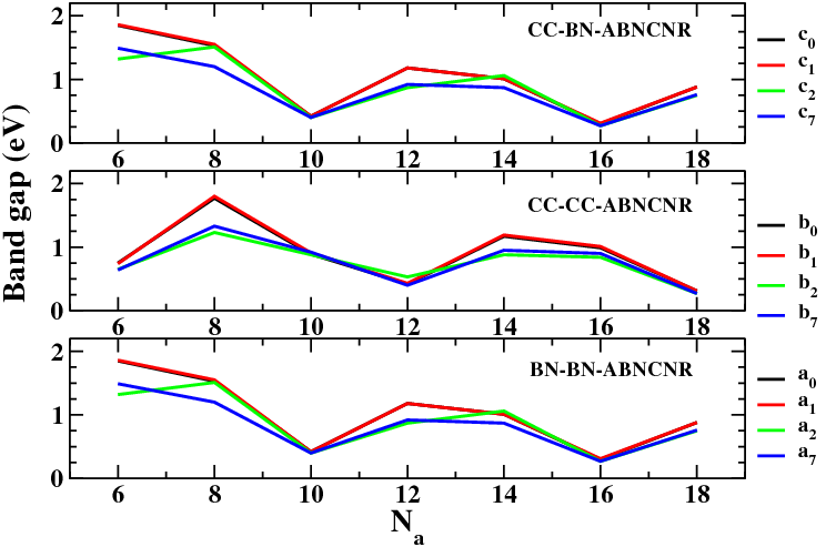
Quantitative calculations presented in the previous sections were performed for nanoribbons with the width . Therefore, the question arises: Will the qualitative features exhibited by ribbons of this width also hold for wider ribbons? To ascertain that we performed calculations for the ribbons with the widths in the range 6, and found that wider CC-BN-ABNCNRs, BN-BN-ABNCNRs, and CC-CC-ABNCNRs exhibit behavior similar to that observed for width . Fig. 18 presents the band gaps of nonmagnetic ABNCNRs, as a function of their width, and Table 8 presents the band gaps of spin-polarized CC-BN-ABNCNRS (c3, c4, c5 and c6). From Fig. 18, we conclude that overall band gaps of nonmagnetic ABNCNRs decrease with the increasing width, in an oscillatory behavior, similar to the cases of AGNRs34 and ABNNRs73. Band structures of all configurations of BN-BN-, CC-CC-, and CC-BN ABNCNRs for width are presented in Figs. 5-7 of the Supporting Information. From Table.8, it is clear that similar to the nonmagnetic ABNCNRs, spin-polarized band gaps (up and down channels) of c3 and c4 configurations also decrease with the increasing the width, while c5 and c6 configurations are metallic for all the widths. Spin-polarized band gaps of CC-CC-ABNCNRs and BN-BN-ABNCNRs are presented in Tables 1 and 2, respectively, of the Supporting Information. Similar to CC-BN-ABNCNRs, the band gaps of spin-polarized configurations of BN-BN (a3) and CC-CC-ABNCNRs(b1-b6) decrease with the increasing width. And, configurations a4-a6 exhibit metallic behavior irrespective of their widths. Thus, we believe that the qualitative features observed for ribbons of width , hold also for much wider ribbons.
| Band gaps (eV) | ||||||||
| c3 | c4 | c5 | c6 | |||||
| Up | Dn | Up | Dn | Up | Dn | Up | Dn | |
| 8 | 1.38 | 0.84 | 1.40 | 0.95 | M | M | M | M |
| 10 | 0.45 | 0.23 | 0.38 | 0.48 | M | M | M | M |
| 12 | 1.08 | 0.74 | 1.09 | 0.80 | M | M | M | M |
| 14 | 1.03 | 0.61 | 1.01 | 1.11 | M | M | M | M |
| 16 | 0.33 | 0.18 | 0.27 | 0.37 | M | M | M | M |
| 18 | 0.88 | 0.57 | 0.86 | 0.65 | M | M | M | M |
4 Conclusions
We performed extensive electronic structure calculations on fully and partially hydrogen-passivated ABNCNRs, using the first-principles based DFT approach, and studied three types of configurations, namely, CC-CC-, BN-BN- and CC-BN-, depending upon the atoms present on their edges. When compared to fully hydrogen-passivated ABNCNRs, partial edge passivation causes the formation of additional energy bands near Fermi-levels of these nanoribbons, leading to different electronic properties. We found that fully hydrogen-passivated, and completely bare ABNCNRs, are non-magnetic semiconductors. However, as far as partially passivated ABNCNRs are concerned, they were found to exhibit a wide range of electronic behavior such as normal metal, magnetic metal, normal semiconductor, and spin-polarized semiconductor, depending on their edge termination, and hydrogenation schemes. We also found that the ABNCNRs with larger widths are more stable compared to the narrower ones. Furthermore, a few their configurations exhibited metallic behavior, for all the widths considered. Thus, in principle, partial hydrogenation of edges allows the tuning of the band structures of ABNCNRs, with possible applications in the fields of spintronics, and optoelectronic devices.
5 acknowledgments
NA and NM gratefully acknowledge the support from Monash HPC, National Computing Infrastructure of Australia, and the Pawsey Supercomputing facility. This research was partially supported by the Australian Research Council Centre of Excellence in Future Low-Energy Electronics Technologies (project number CE170100039) and funded by the Australian Government. AS acknowledges the financial support from Department of Science and Technology, Government of India, under project no. SB/S2/CMP-066/2013.
References
- Novoselov et al. 2004 K. S. Novoselov, A. K. Geim, S. V. Morozov, D. Jiang, Y. Zhang, S. V. Dubonos, I. V. Grigorieva and A. A. Firsov, Science, 2004, 306, 666–669.
- Hu et al. 1999 J. Hu, T. W. Odom and C. M. Lieber, Accounts of chemical research, 1999, 32, 435–445.
- Shuai et al. 1997 Z. Shuai, J. Brédas, S. Pati and S. Ramasesha, Physical Review B, 1997, 56, 9298.
- Coleman et al. 2011 J. N. Coleman, M. Lotya, A. ÓNeill, S. D. Bergin, P. J. King, U. Khan, K. Young, A. Gaucher, S. De, R. J. Smith et al., Science, 2011, 331, 568–571.
- Mannix et al. 2015 A. J. Mannix, X.-F. Zhou, B. Kiraly, J. D. Wood, D. Alducin, B. D. Myers, X. Liu, B. L. Fisher, U. Santiago, J. R. Guest et al., Science, 2015, 350, 1513–1516.
- Wang et al. 2012 Q. H. Wang, K. Kalantar-Zadeh, A. Kis, J. N. Coleman and M. S. Strano, Nature nanotechnology, 2012, 7, 699–712.
- Liu et al. 2014 H. Liu, A. T. Neal, Z. Zhu, Z. Luo, X. Xu, D. Tománek and P. D. Ye, ACS Nano, 2014, 8, 4033–4041.
- Geim and Novoselov 2007 A. K. Geim and K. S. Novoselov, Nature materials, 2007, 6, 183–191.
- Katsnelson 2007 M. I. Katsnelson, Materials today, 2007, 10, 20–27.
- Castro Neto et al. 2009 A. H. Castro Neto, F. Guinea, N. M. R. Peres, K. S. Novoselov and A. K. Geim, Rev. Mod. Phys., 2009, 81, 109–162.
- Rogers 2008 J. A. Rogers, Nature nanotechnology, 2008, 3, 254–255.
- Dean et al. 2010 C. R. Dean, A. F. Young, I. Meric, C. Lee, L. Wang, S. Sorgenfrei, K. Watanabe, T. Taniguchi, P. Kim, K. Shepard et al., Nature nanotechnology, 2010, 5, 722–726.
- Zhou et al. 2009 J. Zhou, Q. Wang, Q. Sun, X. Chen, Y. Kawazoe and P. Jena, Nano letters, 2009, 9, 3867–3870.
- Li et al. 2008 X. Li, X. Wang, L. Zhang, S. Lee and H. Dai, Science, 2008, 319, 1229–1232.
- Yuan et al. 2012 L. Yuan, Z. Li, J. Yang and J. G. Hou, Physical Chemistry Chemical Physics, 2012, 14, 8179–8184.
- Elias et al. 2009 D. Elias, R. Nair, T. Mohiuddin, S. Morozov, P. Blake, M. Halsall, A. Ferrari, D. Boukhvalov, M. Katsnelson, A. Geim et al., Science, 2009, 323, 610–613.
- Sofo et al. 2007 J. O. Sofo, A. S. Chaudhari and G. D. Barber, Physical Review B, 2007, 75, 153401.
- Li et al. 2009 Y. Li, Z. Zhou, P. Shen and Z. Chen, The Journal of Physical Chemistry C, 2009, 113, 15043–15045.
- Gui et al. 2008 G. Gui, J. Li and J. Zhong, Physical Review B, 2008, 78, 075435.
- Wang et al. 2009 X. Wang, X. Li, L. Zhang, Y. Yoon, P. K. Weber, H. Wang, J. Guo and H. Dai, Science, 2009, 324, 768–771.
- Rani and Jindal 2013 P. Rani and V. Jindal, RSC Advances, 2013, 3, 802–812.
- Ci et al. 2010 L. Ci, L. Song, C. Jin, D. Jariwala, D. Wu, Y. Li, A. Srivastava, Z. Wang, K. Storr, L. Balicas et al., Nature materials, 2010, 9, 430–435.
- Bhowmick et al. 2011 S. Bhowmick, A. K. Singh and B. I. Yakobson, The Journal of Physical Chemistry C, 2011, 115, 9889–9893.
- Bernardi et al. 2012 M. Bernardi, M. Palummo and J. C. Grossman, Physical review letters, 2012, 108, 226805.
- Wang et al. 2011 H. Wang, T. Taychatanapat, A. Hsu, K. Watanabe, T. Taniguchi, P. Jarillo-Herrero and T. Palacios, IEEE Electron Device Letters, 2011, 32, 1209–1211.
- Ramasubramaniam et al. 2011 A. Ramasubramaniam, D. Naveh and E. Towe, Nano letters, 2011, 11, 1070–1075.
- Peng and De 2012 Q. Peng and S. De, Physica E: Low-dimensional Systems and Nanostructures, 2012, 44, 1662–1666.
- Pruneda 2010 J. Pruneda, Physical Review B, 2010, 81, 161409.
- Zhang et al. 2015 M. Zhang, G. Gao, A. Kutana, Y. Wang, X. Zou, S. T. John, B. I. Yakobson, H. Li, H. Liu and Y. Ma, Nanoscale, 2015, 7, 12023–12029.
- Xia et al. 2003 Y. Xia, P. Yang, Y. Sun, Y. Wu, B. Mayers, B. Gates, Y. Yin, F. Kim and H. Yan, Advanced Materials, 2003, 15, 353–389.
- Wang and Li 2006 X. Wang and Y. Li, Inorganic Chemistry, 2006, 45, 7522–7534.
- Kosynkin et al. 2009 D. V. Kosynkin, A. L. Higginbotham, A. Sinitskii, J. R. Lomeda, A. Dimiev, B. K. Price and J. M. Tour, Nature, 2009, 458, 872–876.
- Zeng et al. 2010 H. Zeng, C. Zhi, Z. Zhang, X. Wei, X. Wang, W. Guo, Y. Bando and D. Golberg, Nano letters, 2010, 10, 5049–5055.
- Son et al. 2006 Y.-W. Son, M. L. Cohen and S. G. Louie, Phys. Rev. Lett., 2006, 97, 216803.
- Ramasubramaniam 2010 A. Ramasubramaniam, Phys. Rev. B, 2010, 81, 245413.
- Lee and Cho 2009 G. Lee and K. Cho, Physical Review B, 2009, 79, 165440.
- Son et al. 2006 Y.-W. Son, M. L. Cohen and S. G. Louie, Nature, 2006, 444, 347–349.
- Basheer et al. 2011 E. A. Basheer, P. Parida and S. K. Pati, New Journal of Physics, 2011, 13, 053008.
- Barone and Peralta 2008 V. Barone and J. E. Peralta, Nano letters, 2008, 8, 2210–2214.
- Zheng et al. 2008 F. Zheng, G. Zhou, Z. Liu, J. Wu, W. Duan, B.-L. Gu and S. Zhang, Physical Review B, 2008, 78, 205415.
- Dutta et al. 2009 S. Dutta, A. K. Manna and S. K. Pati, Phys. Rev. Lett., 2009, 102, 096601.
- Du et al. 2009 A. Du, Y. Chen, Z. Zhu, G. Lu and S. C. Smith, Journal of the American chemical society, 2009, 131, 1682–1683.
- Kan et al. 2008 E.-J. Kan, X. Wu, Z. Li, X. C. Zeng, J. Yang and J. Hou, The Journal of chemical physics, 2008, 129, 084712.
- Liu et al. 2011 Y. Liu, X. Wu, Y. Zhao, X. C. Zeng and J. Yang, The Journal of Physical Chemistry C, 2011, 115, 9442–9450.
- Huang et al. 2012 B. Huang, H. Lee, B.-L. Gu, F. Liu and W. Duan, Nano Research, 2012, 5, 62–72.
- Liu et al. 2011 Z. Liu, Y. Zhu and Z. Yang, The Journal of chemical physics, 2011, 134, 074708.
- Kaneko et al. 2013 T. Kaneko, K. Harigaya and H. Imamura, Journal of the Physical Society of Japan, 2013, 82, 083710.
- Ouyang et al. 2015 J. Ouyang, M. Long, D. Zhang, X. Zhang, J. He and Y. Gao, Computational Condensed Matter, 2015, 4, 40 – 45.
- Seol and Guo 2011 G. Seol and J. Guo, Applied Physics Letters, 2011, 98, 143107.
- He et al. 2010 J. He, K.-Q. Chen, Z.-Q. Fan, L.-M. Tang and W. Hu, Applied Physics Letters, 2010, 97, 239.
- Sun et al. 2016 Y. Sun, G. Yu, J. Liu, X. Shen, X. Huang and W. Chen, Physical Chemistry Chemical Physics, 2016, 18, 1326–1340.
- Fan et al. 2011 Y. Fan, M. Zhao, X. Zhang, Z. Wang, T. He, H. Xia and X. Liu, Journal of Applied Physics, 2011, 110, .
- Lai and Lu 2011 L. Lai and J. Lu, Nanoscale, 2011, 3, 2583–2588.
- Lu et al. 2011 P. Lu, Z. Zhang and W. Guo, The Journal of Physical Chemistry C, 2011, 115, 3572–3577.
- Prezzi et al. 2008 D. Prezzi, D. Varsano, A. Ruini, A. Marini and E. Molinari, Phys. Rev. B, 2008, 77, 041404.
- Wu et al. 2009 X.-j. Wu, M.-h. Wu and X. C. Zeng, Frontiers of Physics in China, 2009, 4, 367–372.
- Peng et al. 2014 X. Peng, A. Copple and Q. Wei, Journal of Applied Physics, 2014, 116, 144301.
- Alaal et al. 2016 N. Alaal, V. Loganathan, N. Medhekar and A. Shukla, Journal of Physics D: Applied Physics, 2016, 49, 105306.
- Alaal et al. 2017 N. Alaal, V. Loganathan, N. Medhekar and A. Shukla, Physical Review Applied, 2017, 7, 064009.
- Tang et al. 2013 Z.-K. Tang, L.-L. Wang, L.-M. Tang, W.-Q. Huang, D.-Y. Zhang, L. Xu and X.-F. Li, Solid State Communications, 2013, 158, 25 – 28.
- Rai et al. 2015 H. M. Rai, S. K. Saxena, V. Mishra, R. Late, R. Kumar, P. R. Sagdeo, N. K. Jaiswal and P. Srivastava, Solid State Communications, 2015, 212, 19–24.
- Kresse and Furthmüller 1996 G. Kresse and J. Furthmüller, Computational Materials Science, 1996, 6, 15 – 50.
- Fuchs and Scheffler 1999 M. Fuchs and M. Scheffler, Computer Physics Communications, 1999, 119, 67–98.
- Perdew et al. 1996 J. P. Perdew, K. Burke and M. Ernzerhof, Physical review letters, 1996, 77, 3865.
- Wang et al. 2011 S. Wang, Q. Chen and J. Wang, Applied Physics Letters, 2011, 99, 063114.
- Jiang et al. 2013 X. Jiang, N. Kharche, P. Kohl, T. B. Boykin, G. Klimeck, M. Luisier, P. M. Ajayan and S. K. Nayak, Applied Physics Letters, 2013, 103, 133107.
- Manna and Pati 2011 A. K. Manna and S. K. Pati, The Journal of Physical Chemistry C, 2011, 115, 10842–10850.
- Manna and Pati 2013 A. K. Manna and S. K. Pati, Journal of Materials Chemistry C, 2013, 1, 3439–3447.
- Henkelman et al. 2006 G. Henkelman, A. Arnaldsson and H. Jónsson, Computational Materials Science, 2006, 36, 354–360.
- Fang et al. 2014 D. Fang, Y. Zhang and S. Zhang, New Journal of Physics, 2014, 16, 115006.
- Hod et al. 2007 O. Hod, V. Barone, J. E. Peralta and G. E. Scuseria, Nano letters, 2007, 7, 2295–2299.
- Kan et al. 2008 E.-j. Kan, Z. Li, J. Yang and J. Hou, Journal of the American Chemical Society, 2008, 130, 4224–4225.
- Zhang and Guo 2008 Z. Zhang and W. Guo, Phys. Rev. B, 2008, 77, 075403.