Magnetically-defined topological edge plasmons in edgeless electron gas
Topological materials bear gapped excitations in bulk yet protected gapless excitations at boundaries Qi and Zhang (2011); Lu et al. (2014). Magnetoplasmons (MPs), as high-frequency density excitations of two-dimensional electron gas (2DEG) in a perpendicular magnetic field Ando et al. (1982); Kushwaha (2001), embody a prototype of band topology for bosons Jin et al. (2016, 2017). The time-reversal-breaking magnetic field opens a topological gap for bulk MPs up to the cyclotron frequency Zudov et al. (2003); Gao et al. (2016); topologically-protected edge magnetoplasmons (EMPs) bridge the bulk gap and propagate unidirectionally along system’s boundaries Mast et al. (1985); Glattli et al. (1985); Fetter (1986); Volkov and Mikhailov (1988). However, all the EMPs known to date adhere to physical edges where the electron density terminates abruptly Ashoori et al. (1992); Balev and Vasilopoulos (1997); Kumada et al. (2014). This restriction has made device application extremely difficult. Here we demonstrate a new class of topological edge plasmons – domain-boundary magnetoplasmons (DBMPs), within a uniform edgeless 2DEG. Such DBMPs arise at the domain boundaries of an engineered sign-changing magnetic field and are protected by the difference of gap Chern numbers () across the magnetic domains. They propagate unidirectionally along the domain boundaries and are immune to domain defects Jin et al. (2016). Moreover, they exhibit wide tunability in the microwave frequency range under an applied magnetic field or gate voltage. Our study opens a new direction to realize high-speed reconfigurable topological devices Mahoney et al. (2017); Fang et al. (2012); Bahari et al. (2017).
In this work, we present the first experimental observation of a new class of topological edge plasmons, domain-boundary magnetoplasmons (DBMPs), at microwave frequencies in a high-mobility GaAs/AlGaAs heterojunction. In contrast to the traditional wisdom, where edge magentoplasmons (EMPs) must rely on a space-varying electron density , in our scenario, the DBMPs are defined by a space-varying magnetic field embedded into a uniform 2DEG Ye et al. (1995); Nogaret et al. (2000); Reijniers and Peeters (2000); Yasuda et al. (2017). A custom-shaped NdFeB strong permanent magnet, placed immediately above the heterojunction, produces a sign-changing magnetic field around T in magnitude, sufficient to gap bulk MPs in each magnetic domain. The cm2 V-1 s-1 high electron mobility in this system affords an ultra-long relaxation time of hundreds of picoseconds and ultra-low damping rate of only a few gigahertz, superior to any other existing 2DEG systems Mast et al. (1985); Bolotin et al. (2008); Ohtomo and Hwang (2004). By measuring microwave resonant spectra, we clearly verify the existence and nonreciprocal nature of DBMPs. Their excitation frequencies display a unique dependence on both an applied magnetic field and gate voltage, differing substantially from the conventional EMPs in several intriguing aspects. Our theoretical prediction and experimental observation show excellent mutual agreement.
System design Figure 1 illustrates the layout of our magnetoplasmonic device. Conceptually (Fig. 1a), a 2DEG in a GaAs/AlGaAs heterojunction (see Methods) is cladded above and below by a fused silica (glass) spacer and a GaAs substrate, respectively, of thicknesses m and m, and permittivities and . This dielectric-2DEG-dielectric structure is enclosed in a metallic cavity along , terminating at the spacer’s top and substrate’s bottom. A holed NdFeB permanent magnet, atop the upper cavity wall, projects a circular magnetic field onto the 2DEG. The sign of changes abruptly across the projection of the hole’s radius, mm, producing adjacent oppositely-signed magnetic domains (see Methods). The entire 2DEG is additionally exposed to a tunable homogeneous magnetic field from a superconducting coil, allowing an overall shift of the magnetic field profile.
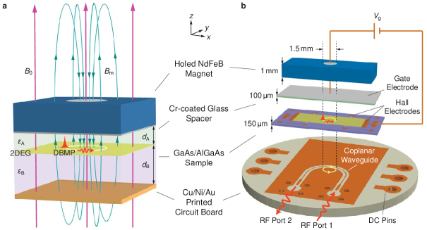
In practice (Fig. 1b), the heterojunction sample has a 12 mm 6 mm rectangular footprint. A 9 mm 3 mm Hall bar is fabricated atop of it, allowing in situ measurements and control of the 2DEG electron concentration . The fused silica spacer is topped by a 100 nm thick e-beam evaporated Cr-coating, serving simultaneously as upper cavity wall and gate electrode Hatke et al. (2015); Mi et al. (2017). A gate voltage of V can be applied across the Cr-coating–Hall bar junction to tune the electron concentration. The sample-spacer-magnet assembly is glued by Poly(methyl methacrylate) (PMMA) onto a customized Cu printed circuit board (PCB) with a 5 m Ni and 200 nm Au surface finish. The PCB hosts a coplanar waveguide (CPW) connecting RF Ports 1 and 2 with mini-SMP connectors Hatke et al. (2015). By design, the CPW has a 50 impedance with the sample-magnet assembly loaded. The CPW signal line is aligned tangentially to the projected circle from the hole of magnet so as to maximize the microwave-DBMP coupling.
Theoretical prediction The main physics of MP system can be captured by the continuity equation and a constitutive equation containing the longitudinal Coulomb force and transverse Lorentz force:
| (1a) | |||
| (1b) | |||
Here, and are the surface current and charge densities, evaluated at frequencies and in-plane positions . is the self-consistent potential due to the (screened) Coulomb interaction . is a space-varying cyclotron frequency, with the electron effective mass. As elaborated below, even with a constant electron density , topologically-protected DBMPs can reside at boundaries of sign-changing magnetic domains solely defined by the spatial profile and Jin et al. (2016).
The total magnetic field, , is the sum of a tunable, uniform field from the superconducting coil, and a fixed, -dependent field from the holed NdFeB permanent magnet. The latter is well-approximated by a step function,
| (2) |
Here, contributes an equal-magnitude sign-changing jump at mm, while accounts for a small, overall shift due to the small distance between magnet and 2DEG. By a combination of finite-element simulations and room-temperature Hall-probe measurements on the surface of magnet, we infer the low-temperature values of each as T and T (see Methods).
The presence of cladding dielectrics and encapsulating metals in this system significantly influences the Coulomb interaction and frequency scale of the problem. In momentum space, the Coulomb interaction takes a screened form,
| (3) |
with being the -dependent screening function Fetter (1986); Volkov and Mikhailov (1988). The scalar potential and surface charge density are related by . The eigenmodes consistent with Eqs. (1) are eigenstates of a Hamiltonian with operator elements Jin et al. (2016, 2017). In the circularly symmetric “potential” of Eq. (2), the eigenmodes decompose according to with azimuthal angle and angular wavenumber . The radial function can be expanded by the Bessel functions with radial wavenumbers , , which enter the Coulomb interaction Eq. (3) (see Methods).
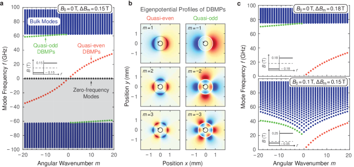
The resulting plasmonic properties are explored in Fig. 2. Figure 2a illustrates the magnetoplasmonic dispersion of bulk MP and DBMP modes for cm-2, T, and T. The spectrum exhibits particle-hole symmetry, i.e. , with a zero-frequency band describing static modes Jin et al. (2016). The bulk MPs in each magnetic domain exhibits a gap from zero frequency to approximately . The band topology of each domain, considered as an extended bulk, is characterized by a topological invariant, the Chern number, equaling Jin et al. (2016). The associated gap Chern number , also equaling in this case, can be identified, whose difference across the domains, , dictates the existence of two unidirectional edge states localized at . These conclusions are clearly manifest in Fig. 2a and 2b from the existence of quasi-even and quasi-odd DBMP branches (so named due to their asymptotic association with the even and odd DBMPs of a linear domain boundary). Both are unidirectional and exhibit increasing localization with incrementing angular wavenumbers . We emphasize that these DBMPs drastically differ from the conventional EMPs by being solely magnetically-engineered. Interestingly, they are topologically equivalent to the equatorial Kelvin and Yanai waves of the ocean and atmosphere (with a Coriolis parameter in place of ) Delplace et al. (2017).
Figure 2c investigates the dispersion for increased (from 0.15 T to 0.18 T) and (from 0 to 0.1 T). Comparing to Fig. 2a, increasing widens the bandgap and decreases the frequencies of the quasi-even DBMPs. Conversely, increasing (but maintaining ) reduces the overall gap—since the cyclotron frequency is lowered in the inner domain—and increases the excitation frequencies of the quasi-even DBMP. This latter behavior further distinguishes our new DBMPs from the traditional EMPs which shift in the opposite direction with increasing Fetter (1986); Mast et al. (1985). The quasi-odd DBMP branch in Fig. 2c appears non-gapless and hence non-topological in the considered range of : this, however, is remedied at larger where the dispersion bends downwards (not shown), instating an asymptotically gapless behavior in deference to the topological requirements.
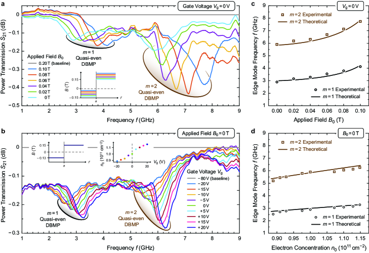
Experimental observation We next seek experimental evidence for the theoretically predicted DBMPs. The device is inserted into a He-3 cryostat running at 0.5 K. An Agilent E5071C Network Analyzer (NA) is used to acquire power transmission (Port 1 to Port 2) and (Port 2 to Port 1) in the frequency range 300 kHz to 20 GHz Hatke et al. (2015); Mi et al. (2017); Mahoney et al. (2017). In practice, however, our focused frequency range is limited to 1 to 10 GHz, beyond which the cables and NA bear too high loss and noise, prohibiting acquisition of clear signals. Referring to Figs. 2a and 2c, we consequently expect to observe characteristic absorption associated with only the and quasi-even DBMPs.
In the first series of measurements, we keep the gate grounded, V, and investigate the influence of the applied magnetic field on the resonant absorption of quasi-even DBMPs in (Fig. 3a). All signals are divided by a reference (denoted baseline). Here, we choose T as baseline, which provides a high suppression of unwanted low-frequency bulk modes, without exerting too great a torque on the magnet–sample assembly. For every -spectrum in Fig. 3a, each reflecting a single applied field in the range to T, we observe two well-defined absorptive resonances, corresponding to the right-circulating quasi-even DBMPs. Spanning frequencies from 3 to 4 GHz and 6 to 8 GHz, they exhibit linewidths of approximately 1 to 2 GHz, roughly consistent with the Hall-probe inferred DC damping rate GHz. Figure 3c compares the measured and theoretically predicted resonance frequencies. First, we observe the excellent mutual agreement in the absence of fitting parameters. Second, we emphasize the monotonously increasing excitation frequencies with increasing , which unambiguously differentiates our magnetically-defined DBMPs from the conventional EMPs.
In the second series of measurements, we fix the applied magnetic field T, and explore the DBMPs’ dependence on the gate voltage (Fig. 3b). The baseline is chosen at V, which corresponds to an essentially electron-depleted 2DEG supporting no plasmonic modes. Once more, every spectrum in Fig. 3b, each now corresponding to distinct gate voltages in the range to V, exhibits two clear absorptive resonances associated with the quasi-even DBMPs. Increasing the gate voltage (or, equivalently, the electron concentration ) increases the DBMP frequency, as expected. Moreover, the extinction depth of each resonance also increases with the . This is consistent with the -sum rule Yang et al. (2015) which dictates a linear increase of integrated extinction with increased (disregarding the negligible spectral dispersion in the microwave-DBMP coupling). Comparing theoretical and experimental observations, in Fig. 3d, we once again find excellent agreement.
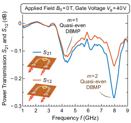
Finally, in Fig. 4, we examine the nonreciprocal properties of the DBMPs in order to explicitly demonstrate the underlying unidirectional character of the DBMPs. Since the DBMPs are right-circulating in the bandgap (Fig. 2), and correspond to the “easy-coupling” and “hard-coupling” directions, respectively, of our device (Fig. 1b). Each coupling direction is normalized separately, with baselines taken at T. The 2DEG is gated by V, ensuring a pronounced extinction depth, and the applied magnetic field is turned off T. In this configuration, the and quasi-even DBMPs exist at 4.2 GHz and 8.0 GHz, respectively. Comparing and we observe distinct asymmetry of extinction depth at each resonance, with exhibiting shallower extinction. This asymmetry is indicative of the unidirectional character of the DBMPs. The observed isolation ratio is small because of the wavelength mismatch between the microwaves in CPW and the DBMPs along the circle. This is mainly a limitation from the CPW evanescent-coupling technique. A fuller assessment of the isolation capabilities could more naturally be enabled by point-source excitation Ashoori et al. (1992); Wang et al. (2009); Fei et al. (2011); Kumada et al. (2014).
Conclusion We have for the first time realized a new class of topologically-protected edge plasmons, domain-boundary magnetoplasmons, embedded in an edgeless 2DEG. They situate at magnetically-defined domain boundaries, and are topologically distinct from the conventional edge magnetoplasmons. We have experimentally observed and characterized these new DBMPs at microwave frequencies in a high-mobility GaAs/AlGaAs heterojunction under a custom-shaped NdFeB permanent magnet. Our experimental results show remarkable agreement with theoretical calculations. The demonstrated DBMP architecture, if packed with denser magnetic patterns, can be extended to higher frequencies and finer scales, and shall pave the way towards high-speed reconfigurable topological devices Mahoney et al. (2017); Fang et al. (2012); Bahari et al. (2017).
Acknowledgements D.J., Y.X., S.W., K.Y.F., Y.W. and X.Z. acknowledge support from AFOSR MURI (Grant No. FA9550-12-1-0488) and Office of Sponsored Research (OSR) (Award No. OSR-2016-CRG5-2950-03). T.C. acknowledges support from the Danish Council for Independent Research (Grant No. DFF–6108-00667). The National High Magnetic Field Laboratory (NHMFL) is supported by NSF Cooperative Agreement (No. DMR-0654118), the State of Florida, and the DOE. M.F. and L.E., and Microwave Spectroscopy Facility are supported by the DOE (Grant No. DE-FG02-05-ER46212). G.C.G. and M.J.M. acknowledge support from the DOE Office of Basic Energy Sciences, Division of Materials Sciences and Engineering (Award No. DE-SC0006671), the W. M. Keck Foundation, and Microsoft Station Q. Q.H. and N.X.F. are supported by AFOSR MURI (Grant No. FA9550-12-1-0488).
References
- Qi and Zhang (2011) X.-L. Qi and S.-C. Zhang, Rev. Mod. Phys. 83, 1057 (2011).
- Lu et al. (2014) L. Lu, J. D. Joannopoulos, and M. Soljačić, Nat. Photon. 8, 821 (2014).
- Ando et al. (1982) T. Ando, A. B. Fowler, and F. Stern, Rev. Mod. Phys. 54, 437 (1982).
- Kushwaha (2001) M. S. Kushwaha, Surf. Sci. Rep. 41, 1 (2001).
- Jin et al. (2016) D. Jin, L. Lu, Z. Wang, C. Fang, J.D. Joannopoulos, M. Soljačić, L. Fu, and N.X. Fang, Nat. Commun. 7, 13486 (2016).
- Jin et al. (2017) D. Jin, T. Christensen, M. Soljačić, N. X. Fang, L. Lu, and X. Zhang, Phys. Rev. Lett. 118, 245301 (2017).
- Zudov et al. (2003) M. Zudov, R. Du, L. Pfeiffer, and K. West, Phys. Rev. Lett. 90, 046807 (2003).
- Gao et al. (2016) W. Gao, B. Yang, M. Lawrence, F. Fang, B. Béri, and S. Zhang, Nat. Commun. 7, 12435 (2016).
- Mast et al. (1985) D. B. Mast, A. J. Dahm, and A. L. Fetter, Phys. Rev. Lett. 54, 1706 (1985).
- Glattli et al. (1985) D. Glattli, E. Andrei, G. Deville, J. Poitrenaud, and F. Williams, Phys. Rev. Lett. 54, 1710 (1985).
- Fetter (1986) A. L. Fetter, Phys. Rev. B 33, 5221 (1986).
- Volkov and Mikhailov (1988) V. A. Volkov and S. A. Mikhailov, Sov. Phys. JETP 67, 1639 (1988).
- Ashoori et al. (1992) R. C. Ashoori, H. L. Stormer, L. N. Pfeiffer, K. W. Baldwin, and K. West, Phys. Rev. B 45, 3894 (1992).
- Balev and Vasilopoulos (1997) O. Balev and P. Vasilopoulos, Phys. Rev. B 56, 13252 (1997).
- Kumada et al. (2014) N. Kumada, P. Roulleau, B. Roche, M. Hashisaka, H. Hibino, I. Petković, and D. Glattli, Phys. Rev. Lett. 113, 266601 (2014).
- Mahoney et al. (2017) A. Mahoney, J. Colless, S. Pauka, J. Hornibrook, J. Watson, G. Gardner, M. Manfra, A. Doherty, and D. Reilly, Phys. Rev. X 7, 011007 (2017).
- Fang et al. (2012) K. Fang, Z. Yu, and S. Fan, Nat. Photon. 6, 782 (2012).
- Bahari et al. (2017) B. Bahari, A. Ndao, F. Vallini, A. El Amili, Y. Fainman, and B. Kanté, Science 358, 636 (2017).
- Ye et al. (1995) P. D. Ye, D. Weiss, R. R. Gerhardts, M. Seeger, K. von Klitzing, K. Eberl, and H. Nickel, Phys. Rev. Lett. 74, 3014 (1995).
- Nogaret et al. (2000) A. Nogaret, S. J. Bending, and M. Henini, Phys. Rev. Lett. 84, 2231 (2000).
- Reijniers and Peeters (2000) J. Reijniers and F. M. Peeters, J. Phys.: Cond. Matter 12, 9771 (2000).
- Yasuda et al. (2017) K. Yasuda, M. Mogi, R. Yoshimi, A. Tsukazaki, K. Takahashi, M. Kawasaki, F. Kagawa, and Y. Tokura, Science 358, 1311 (2017).
- Bolotin et al. (2008) K. Bolotin, K. Sikes, J. Hone, H. Stormer, and P. Kim, Phys. Rev. Lett. 101, 096802 (2008).
- Ohtomo and Hwang (2004) A. Ohtomo and H. Hwang, Nature 427, 423 (2004).
- Hatke et al. (2015) A. Hatke, Y. Liu, L. Engel, M. Shayegan, L. Pfeiffer, K. West, and K. Baldwin, Nat. Commun. 6 (2015).
- Mi et al. (2017) J. Mi, H. Liu, J. Shi, L. Pfeiffer, K. West, K. Baldwin, and C. Zhang, arXiv preprint arXiv:1708.08498 (2017).
- Delplace et al. (2017) P. Delplace, J. Marston, and A. Venaille, Science 358, 1075 (2017).
- Yang et al. (2015) Z.-J. Yang, T. Antosiewicz, R. Verre, F. García de Abajo, S. Apell, and M. Käll, Nano Lett. 15, 7633 (2015).
- Wang et al. (2009) Z. Wang, Y. Chong, J. D. Joannopoulos, and M. Soljačić, Nature 461, 772 (2009).
- Fei et al. (2011) Z. Fei, G.O. Andreev, W. Bao, L.M. Zhang, A.S. McLeod, C. Wang, M.K. Stewart, Z. Zhao, G. Dominguez, M. Thiemens, M.M. Fogler, M.J. Tauber, A.H. Castro Neto, C.N. Lau, F. Keilmann, and D.N. Basov, Nano Lett. 11, 4701 (2011).
- García et al. (2000) L. García, J. Chaboy, F. Bartolomé, and J. Goedkoop, Phys. Rev. Lett. 85, 429 (2000).
- Strnat et al. (1985) K.J. Strnat, D. Li, and H. Mildrum, in Proc. 8th Int. Workshop on Rare Earth Magnets and Their Applications (1985) p. 575.
- (33) TECHNotes of Arnold Corporation, www.arnoldmagnetics.com .
- Abramowitz and Stegun (1972) M. Abramowitz and I.A. Stegun, Handbook of Mathematical Functions with Formulas, Graphs, and Mathematical Tables (Dover, 1972).
Methods
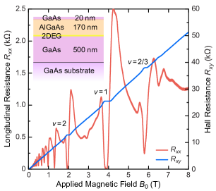
2DEG sample growth and characterization Our sample is a single-interface GaAs/AlxGa1-xAs () heterojunction grown by molecular beam epitaxy (MBE) on a 500 m thick GaAs wafer. After the growth, the sample is back-polished down to 100 m thick in order to enhance the evanescent microwave coupling. The MBE growth consists of a 500 nm thick GaAs layer followed by a 170 nm thick AlxGa1-xAs () spacer and a 20 nm GaAs cap layer to prevent oxidization of the AlGaAs barrier. It is delta-doped with Si doping concentration cm-2 at a setback of 120 nm above the GaAs/AlGaAs interface containing 2DEG. The 2DEG lies 190 nm below top surface. The electron concentration cm-2 and mobility cm2V-1s-1 are extracted from our Hall measurement at K in dark. In our actual microwave experiment at 0.5 K, the typical zero-gate electron concentration is measured to be about cm-2. This number is used in our calculation. The uniform magnetic field is supplied by a superconductor coil. In the absence of the holed NdFeB magnet, it can safely reach above 7 T, enabling a quantum-Hall measurement to characterize the sample (see Fig. 5). When the NdFeB magnet is present, the applied field is limited by practical concerns to at most 0.5 T, beyond which a huge magnetic torque is exerted onto the magnet, risking damage to the sample underneath.
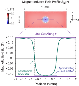
NdFeB magnet design and characterization The NdFeB magnet is 10 mm long, 4 mm wide, and 1 mm thick, and the hole radius is 0.75 mm. It is produced by sintering NdFeB powders in a custom mold and subsequently magnetizing it along the thickness direction. At room temperature, Hall-probe measurements indicate that the holed magnet provides approximately T remanent magnetic field in the surface area inside and outside the hole. With this value, and taking into account the known anisotropic reduction of the magnetism of NdFeB at cryogenic temperatures García et al. (2000); Strnat et al. (1985); TEC , we are able to simulate out the magnetic field profile over the entire magnet at low temperature (see Fig. 6) using a finite-element software (Comsol Multiphysics). From the results, we infer that the two key parameters of Eq. (2) in the main text, namely, a sign-changing field strength T and a overall shift T. These are the values used in our theoretical calculations in Fig. 2c and 2d of the main text, demonstrating excellent agreement between theory and experiment with no fitting parameters.
Theoretical development and calculation scheme The domain-boundary magnetoplasmon (DBMP) modes in our device can be accurately calculated. The evanescent nature of DBMPs and the presence of encapsulating metals, which screen away the long-range part of Coulomb interaction, allow us to focus on the region around and inside the circle mm. We can legitimately take a circularly-symmetric model system cut off at a radius mm , where the scalar potential is grounded . This rigid boundary condition does not affect the DBMPs far inside.
The associated eigenproblem is most conveniently expressed in the chiral representation Jin et al. (2016),
| (4a) | ||||
| (4b) | ||||
| (4c) | ||||
The basic field components are the right-circulating current , the left-circulating current , and the “scalar-potential (density-fluctuation)” current . Here, is a characteristic plasmon frequency, is the -dependent cyclotron frequency, and is the Coulomb integration operator,
| (5) |
with being the screened Coulomb interaction in real space, which does not have a simple form.
The eigensolutions with a given angular wavenumber and obeying the hard-wall boundary condition are linear expansion of Bessel functions,
| (6) |
Here resembles a spin index referring to the , , components, respectively. are discretized radial wavenumbers in which is the th zero of the th order Bessel function . The expansion is practically cutoff at a large finite up to a desired spectral resolution. (In our calculations, we use .) With such discretized cylindrical-wave bases, we can rigorously prove that the screened Coulomb interaction relates and by , where follows Eq. (3) in the main text.
The matrix-form eigenequation in the cylindrical-wave bases reads
| (7) |
Here , is an identity matrix, is an full matrix determined by the magnetic-field profile. If , then is diagonal with the constant cyclotron frequency , and the usual bulk MP modes can be recovered Jin et al. (2016).
The generally radially-varying magnetic field in our problem results in scattering between different radial index (within the and chiral subspace though) and hence localization of new edge modes at the magnetic-domain boundary. We can find the matrix via the expansion
| (8a) | |||
| (8b) | |||
in which are the elements of . Upon laborious calculations involving Bessel integrals Abramowitz and Stegun (1972), we can get
| (9) |
where and are matrices too, whose elements are
| (10a) | ||||
| (10b) | ||||
where and .
Author Contributions D.J. and Y.X. designed the experiment and fabricated the device. D.J. and T.C. performed the calculation and drafted the manuscript. Y.X., S.W. and K.Y.F. tested the device. D.J. and M.F. carried out the measurement. G.C.G., S.F. and Q.H. grew and processed the MBE samples. Y.W., L.E., M.J.M., N.X.F. and X.Z. provided the guidance and joined the discussion. X.Z. led the project. All authors contributed to the manuscript.