Anisotropic electronic transport and Rashba effect of the two-dimensional electron system in (110) SrTiO3-based heterostructures
Abstract
The two-dimensional electron system in Al2O3-δ/SrTiO3 heterostructures displays anisotropic electronic transport. Largest and lowest conductivity and electron mobility are observed along the and direction, respectively. The anisotropy of the sheet resistance and likewise leads to a distinct anisotropic normal magnetotransport () for K. However, at temperatures K and magnetic field T is dominated by weak antilocalization. Despite the rather strong anisotropy of the Fermi surfaces, the in-plane anisotropic magnetoresistance () displays two-fold non-crystalline anisotropy. However, the -amplitude is found to be anisotropic with respect to the current direction, leading to a 60% larger amplitude for current along the direction compared to parallel to . Tight binding calulations evidence an anisotropic Rashba-induced band splitting with dominant linear -dependence. In combination with semiclassical Boltzmann theory the non-crystalline is well described, despite the anisotropic Fermi surface.
pacs:
77.84.Bw,73.43.Qt,73.40.-c,73.20.-rI Introduction
The two-dimensional electron system (2DES) formed at the interface of
the band insulators LaAlO3 (LAO) and SrTiO3 (STO) displays many
intriguing features such as superconductivity, spin-orbit interaction (SOI)
and multiple quantum criticality 1 ; 2 ; 3 , and has thus made LAO/STO a
prototypical system for studying low-dimensional strongly correlated electron
systems. Magnetic properties are reported alike 4 , however, believed to
arise rather from extrinsic sources like oxygen vacancies and strain.
In (001) oriented LAO/STO the sheet carrier concentration can be tuned by
electric field gating through a Lifshitz transition 5 occurring at a
critical sheet carrier concentration cm-2,
where itinerant electrons change from populating only Ti derived 3d
orbitals with symmetry to occupying also the
, orbitals. These bands result in a highly elliptical
Fermi
surface oriented along crystalline directions and may give reason for the
observation of crystalline anisotropic electronic properties. In addition,
localized magnetic moments, pinned to specific orbitals may lead to
crystalline
anisotropy as well and may complicate anisotropic electronic transport. The
coexistence of localized charge carriers close to the interface and itinerant
electrons may lead to fascinating phenomena such as non-isotropic
magnetotransport or magnetic exchange. However, it is not clear whether
interaction between these localized magnetic moments and mobile charge
carriers really happens.
The SOI in (001) LAO/STO results in a non-crystalline two-fold anisotropic
in-plane magnetoresistance () 6 . Interestingly,
for sometimes
a more complex with a four-fold crystalline anisotropy
is reported which
is discussed in terms of a tunable coupling between itinerant
electrons and electrons localized in
orbitals at Ti vacancies7 . However, the appearance of a
crystalline with increasing is not always evident
and rises question
about its microscopic origin. More recently, a giant crystalline
of up
to 100% was reported in (110) oriented LAO/STO 8 . Here, was
about
cm-2. However, the was
supposed to be related to strong
anisotropic spin-orbit field and the anisotropic band structure of (110)
LAO/STO.
With respect to both, namely fundamental aspects such as the possible
simultaneous
appearance of magnetism and superconductivity and applications in the field
of spintronics, a more fundamental knowledge about the origin of anisotropic
magnetotransport is highly desired. Measurements of the
in a rotating
in-plane magnetic field are well suited to probe crystalline anisotropy and
symmetry of a 2DES and are a promising tool to elucidate magnetic properties
because of its high sensitivity towards spin-texture and spin-orbit
interaction 9 .
In order to investigate the microscopic origin of the anisotropic electronic
properties of the 2DES of STO-based heterostructures we studied in detail
the electronic transport of the 2DES formed at the interface of
spinel-type Al2O3-δ and (110) oriented STO (AO/STO). The presence
of oxygen vacancies 10 promoting localized electrons in
combination
with the anisotropic band structure of (110) STO surface 11 makes (110)
AO/STO very suitable for these experiments. The heterostructures were produced
by standard pulsed laser deposition, and characterization of the electronic
transport was done by sheet resistance measurements. Band structure
calculations
were carried out using linear combination of atomic orbitals (LCAO)
approximation to model band structure and Fermi surface properties of
(110) AO/STO. was deduced using
semi-classical Boltzmann theory. Surprisingly, despite the anisotropy of the
electronic band structure and SOI, and the presumably
large content of oxygen vacancies as compared to LAO/STO, we did not observe
indications for a crystalline in (110) AO/STO. The
displays two-fold non-crystalline anisotropic behavior.
Contributions to the electronic transport from the different Fermi surface
sheets as well as the anisotropy of the Fermi surfaces itself are sensitively
affected by .
II Experimental
Sample preparation has been carried out by depositing Al2O3-δ films
onto oriented STO substrates
with a thickness of about 15 nm at a substrate temperature of
by pulsed laser deposition 12 . In order to achieve
an atomically flat, single-type terminated substrate surface, the substrates
are annealed at for 5h in flowing oxygen.
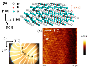
The STO
surface can be terminated by a SrTiO or an oxygen layer, see
Fig. 1 (a), where
the cation composition at the interface should be always the same in case of
single-type termination. Annealing results in a stepped surface topography
with a step height of about Å and a step width of 80 nm, see Fig.
1 (b).
Oxygen partial pressure during Al2O3-δ deposition and
cool-down process was
mbar. Prior to the deposition, microbridges with
a
length of m and a width of m in Hall bar geometry have been
patterned along specific crystallographic directions using a CeO2 hard mask
technique 13 , see Fig. 1 (c).
The microbridges are labeled from A to E, with angle
, and
towards the direction, i.e.,
A and E parallel to and direction, respectively.
The sheet resistance was measured using a physical property measurement system (PPMS) from Quantum Design in the temperature and magnetic field ranges K K and T. To avoid charge carrier activation by light 14 ; 15 , alternating current measurements (A) were started not before 12 hours after loading the samples to the PPMS. The magnetoresistance, , and the , have been measured with magnetic field normal () and parallel () to the interface, respectively. For measuring with rotating in-plane magnetic field , a sample rotator was used. The angle between and -direction was varied from . Special care has been taken to minimize sample wobbling in the apparatus. Residual tilts () of the surface normal with respect to the rotation axis which produces a perpendicular field component oscillating in sync with could be identified by comparison of for different microbridges and could therefore be corrected properly.
III Results and Discussion
III.1 Temperature dependence of the anisotropic electronic transport
The anisotropic electronic band structure of the 2DES found in oriented
LAO/STO heterostructures 8 and at the reconstructed surface of
oriented STO 11 obviously lead to anisotropic electronic transport
16 ; 17 . The lowest electronic subbands along the
direction (along ) display much weaker dispersion and smaller
band-width compared to
the direction (along ) which typically results in larger
resistance
for current direction along the direction 17 ; 8 . The
electronic transport in AO/STO displays distinct anisotropy as well.
The -dependence of the sheet resistance along different
crystallographic
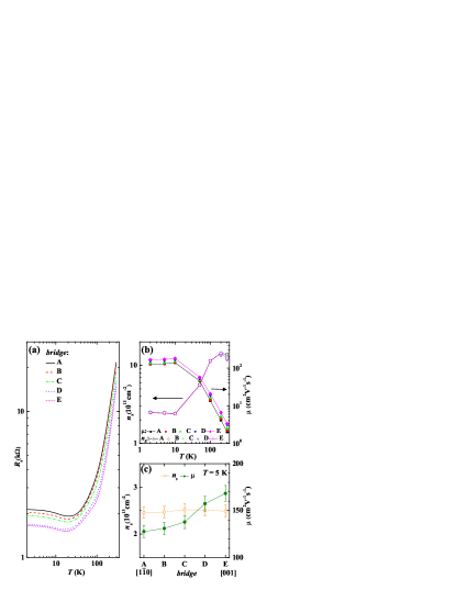
directions is shown in Fig. 2 (a). For all the microbridges,
decreases
with deceasing nearly down to about 100 K and shows a shallow
minimum
around 20 K. The -dependence is very similar to that observed in
AO/STO
and is likely explained by strong renormalization due to electron-phonon
interaction and impurity scattering 18 ; 19 . The resistivity ratio
between 300 K and 10 K amounts to about 20, which is nearly the same as
that of AO/STO. steadily decreases from A
() to E () with
increasing at constant
throughout the complete -range. Obviously, anisotropic transport is not only
restricted to low temperatures , where usually impurity
scattering dominates . Moreover, the anisotropy between A and E,
is largest at K amounting to 47% and
decreases with decreasing to 29% at K. This rather small
-dependence
indicates that the intrinsic anisotropic electronic band structure is very
likely the dominant source for the anisotropic transport. In contrast,
anisotropic transport in AO/STO is extrinsic in nature and
is found only at low where it is
caused mainly by anisotropic impurity scattering
due to an inhomogeneous distribution
of lattice dislocations 20 . With respect to these results,
anisotropy in AO/STO may be diminished at low and intrinsic
anisotropy would be even larger.
In order to extract sheet carrier density and mobility ,
Hall measurements have been carried out in a magnetic field
TT
applied normal to the interface for KK. For K, the
Hall resistance becomes slightly nonlinear, indicating multi-type
carrier transport. However, which we determined from the asymptotic
value of at high fields, i.e., the total , usually deviates by
less than 10% from extracted from in the limit of .
In Fig. 2 (b) the total and the Hall mobility, calculated by
, where is the elementary charge,
are shown as functions of . decreases with decreasing from about
cm-2 at K to cm-2 at
K and is well comparable to that of LAO/STO 10 .
In contrast to the -dependence of , increases from about
cmVs with decreasing to cmVs. The
-dependence of
and is well comparable to that observed in 2DES of STO
based heterostructures 21 ; 22 ; 20 . As expected from the maximum
anisotropy of and is observed at K amounting to 16% and
65%, respectively, and decreases to 2% and 34% at K. Therefore, the
anisotropy of at low is mainly caused by the anisotropy of ,
whereas
for the different microbridges AE are roughly the same. The superior role
of with respect to electronic anisotropy is demonstrated in
Fig. 2 (c)
where and are plotted for AE at = 5K. differs only
little
for the different microbridges. In contrast, steadily increases from A
to E with increasing and shows the highest mobility for bridge E,
i.e., along the direction. The results are reasonable with respect
to the anisotropic band structure and Fermi surface of AO/STO, which
will be discussed in more detail in III. C.
III.2 Magnetotransport
Measurements of the and with magnetic
field direction normal or parallel
to the interface, respectively, are often used to characterize SOI in
low-dimensional electron systems. In STO-based 2DES, the Rashba-type SOI
usually leads to a weak antilocalization (WAL) of the charge carrier transport
at low 2 , resulting in a logarithmic -dependence of
23 .
However, the quantum coherence can be destroyed by applying moderate magnetic
fields leading to a distinct positive 24 .
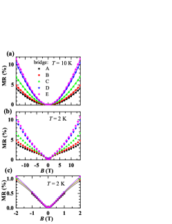
For K the of AO/STO is rather small,
less than 2%, and
displays no distinct anisotropy with respect to the crystallographic direction.
For K, starts to increase with respect to
amplitude and anisotropy.
In Fig. 3, is shown for the microbridges AE,
for K and K.
For K, is positive and amounts to about 10%.
The -dependence of
indicates orbital motion of free carriers due to the
Lorentz force, i.e.,
classical Lorentz scattering (LS) as the dominant scattering mechanism, where
is well described by the Kohler form:
,
with the zero-field resistance 25 . Fits to
the Kohler form are shown by solid lines in Fig. 3 (a).
displays clear anisotropic behavior with respect to the
microbridges, showing a systematic increase from A to E. This is very likely
related to the decrease of the zero-field resistance from A to E, see
Fig. 2 (a).
For K, an additional contribution to the positive
appears. However, significant changes to are restricted
to the low field region, T.
As mentioned above, in 2DES charge transport in the diffusive regime is well
described by the 2D WAL theory23 . The quantum corrections to the
conductivity arise from the interference of
electron waves scattered along closed paths in opposite directions. Phase
coherence is destroyed if the applied magnetic field which results in a phase
shift between the corresponding amplitudes
exceeds a critical value. An estimation for the field limit
can be deduced from the electron mean free path
of the sample. For our sample we obtain nm which results in a field
limit of about 2 T.
Zeeman corrections to the WAL are taken into account by the Maekawa and
Fukuyama (MF)
theory 24 , which is usually used to describe the -dependence of the
in LAO/STO and AO/STO 2 ; 20 . The parameters of the
MF-expression are
the inelastic field , the spin-orbit field , and the electron
g-factor which enters into the Zeeman corrections.
For T, at K is well described by LS and WAL.
Fits to the data, using the MF-based expression given in 2 in
combination with a Kohler term, are shown in Fig. 3 (b) and (c)
by solid lines.
The WAL fitting results in parameters mT and
T. Within the experimental resolution and the limited field range WAL effect appears to be nearly the same for all the microbridges.
Zeeman corrections to
have been found to play only a minor role for the applied
magnetic fields. The magnitude of and are well comparable to
those found in AO/STO and LAO/STO,
where Rashba-type SOI has been identified as the dominant source of spin orbit
coupling.
In comparison to WAL, contributions from LS to at
K are rather small for
T. However, for T, where WAL can usually be neglected,
LS dominates again.
Interestingly, in comparison to the anisotropy of with
respect to the
microbridges for T and at K, the anisotropy of
at 2 K, is
slightly decreased. In contrast, the anisotropy of , , and
with respect
to the current direction, are well comparable for K and 2K, or even
slightly larger at 2K and likely do not explain that behavior.
It might be suggested, that Rashba-type SOI not only influences
by
WAL at low magnetic fields but also at higher fields, where WAL
should be absent.
Anisotropic Rashba splitting was indeed observed by angle resolved
photoemission (ARPES) experiments on STO surfaces 11 and
discussed for (110) LAO/STO
heterostructures 8 ; 16 .
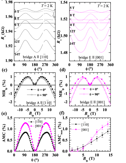
The influence of SOI and Rashba effect on magnetotransport can be studied
more specific,
if the magnetic field is applied parallel to the interface where changes of
the by WAL are negligible.
Applying the magnetic field parallel to the interface at an angle with
respect to the direction, , results in a strong
field-induced directional anisotropy of the resistance , i.e.,
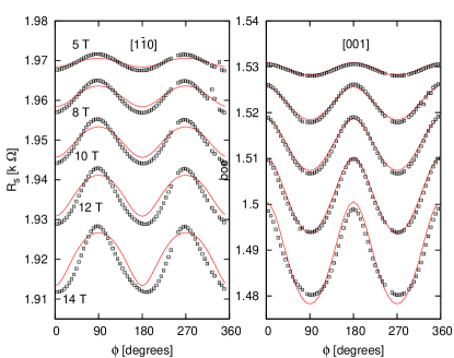
an . Fig. 4 (a) and (b) document
versus for
different at K for bridge A and E, respectively.
shows a sinusoidal oscillating two-fold anisotropic behavior
with maxima at and
for A and E, respectively. Obviously, the anisotropy depends much stronger on
the angle between the direction of the bridge, i.e., the direction of
current and than on the crystallographic direction. Maxima of
are always observed for parallel to the microbridge,
i.e., current flow direction.
Similar anisotropic behavior was also found in LAO/STO and AO/STO.
In the framework of the Drude-Boltzmann theory it was shown, that a
Rashba-type SOI in LAO/STO induces a two-fold non-crystalline
anisotropy in the magnetoconductance 6 , i.e.,
, where the amplitude of the oscillations should scale for
moderate field strength with the square of the spin-orbit energy, i.e.,
, where
and the angle between and .
Therefore, it is very likely, that the observed anisotropy of
is caused by Rashba-type SOI alike.
The amplitude of the oscillations of increases with
increasing magnetic field reaching an of about 1% for A, i.e., along
the direction and 1.4% for E, parallel to the direction
for T. The different amplitudes likely indicate an anisotropic Rashba-type SOI.
Note that the is about one order of magnitude smaller
as compared to the .
Interestingly, first increases with increasing up to about T
and then decreases again. This behavior is documented in more detail in
Fig. 4 (c) and (d) where the in-plane magnetoresistance
is plotted for
A and E versus for field direction parallel () and
perpendicular () to the current direction.
The for is only slightly
larger compared to . With increasing , the
first
increases, displaying a maximum positive magnetoresistance around T. Then,
the decreases and even becomes negative for
above about T. The negative at large
fields possibly results from spin-polarized bands due to Zeeman effect,
leading to a suppression of interband scattering with increasing
27 .
Fig. 4 (e) shows the anisotropic magnetoconductance
versus
for and at T and
K. The maxima of the magnetoconductance oscillations always
appear at and , i.e., perpendicular
to the current direction. For the direction amounts to
about 1.3% and is distinctly larger compared to that of the
direction ().
The field dependence of the amplitude for the two orthogonal
directions is shown in Fig. 4 (f). Measurable magnetoconductance
appears
for T and increases with field to 1.2% and 0.9% at T for
the and direction, respectively.
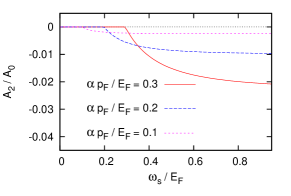
Rashba effect seems to increase with increasing and to be anisotropic with respect to crystallographic direction.
In contrast to the non-crystalline of AO/STO
shown here, a giant crystalline was reported for
LAO/STO - displaying comparable and - with resistance maxima for
along the direction, independent of current
direction 8 .
III.3 Theoretical modeling of the electronic band structure and magnetotransport
In order to obtain a better understanding of the measured electronic transport,
especially the behavior, we carried out
tight-binding calculations to model the electronic subbandstructure of
AO/STO. Details to the linear combination of atomic orbitals (LCAO)
calculations are given in the Appendix. The calculation yields the
energy bands where is the band index and
the wave vector in the rectangular Brillouin zone.
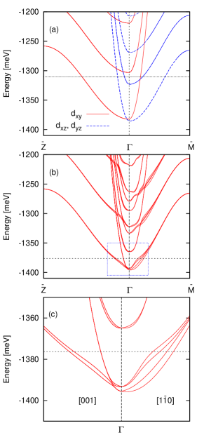
Figure 5 shows the band structure obtained in this way.
The topmost panel shows the band structure
in the absence of spin orbit coupling and symmetry breaking electric field,
which roughly agrees with the band structure obtained by Wang et al.
from a fit to their ARPES data11 (the reason for the deviation
is our modification of the nearest neighbor hopping for bonds
in -direction, see the discussion in the Appendix).
Since there is no mixing between the three orbitals
the bands can be classified according to the type of -orbital
from which they are composed, whereby the bands derived from the
and orbitals are degenerate.
The dashed horizontal line gives the Fermi energy
for an electron density of /unit-cell or
cm-2. This is considerably
higher than the electron densities studied here but
corresponds roughly to the experiments by Wang et al.11 .
In the Figure one can identify
the various subbands generated by the confinement of the electrons
perpendicular to the interface. This hierarchy of subbands in fact extends to
considerably higher energies than shown in the Figure.
The two lower panels show the band structure for finite spin-orbit coupling
and symmetry breaking electric field, but .
One can recognize the two different manifestations of the Rashba effect
discussed already by Zhong et al. Zhong : the splitting of bands
near which can be either or
(see below) and the opening of gaps. The formation of gaps
is particularly obvious at where
the lowest -derived band along combines
with one of the -derived bands along
to form a mixed band whose minimum is shifted upward
by meV.
The dashed horizontal line in the lower two panels gives
for an electron density of /unit-cell or cm-2
which is roughly appropriate for our experiment. We have verified that varying
the density in the range /unit-cell /unit-cell
does not have a significant influence on the magnetoresistance
discussed below. From now
on the labeling of bands is according to their energy i.e.
the lowest band is labeled 1 and so on.
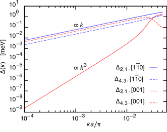
Figure 6 shows the differences
and demonstrates
the power-law behaviour of the Rashba-induced band splitting
for small . Thereby the splitting along
is linear, i.e.
with meV and meV, whereas
along the splitting between
bands and still has this form with meV
whereas the splitting between bands and now is cubic,
meV.
This highlights the anisotropy of the Rashba-effect at the
AO/STO interface.
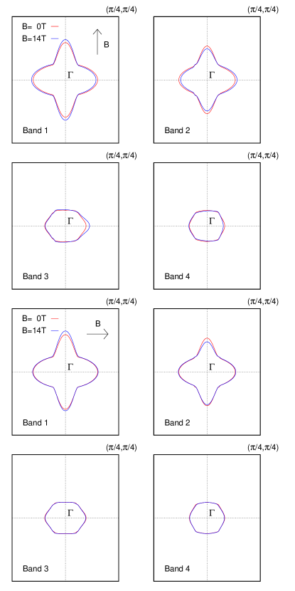
Figure 7 compares the Fermi surfaces for /unit
cell in zero magnetic field and a field of Tesla.
All panels show the square
,
the field direction is along (along )
in the top four (bottom four) panels.
In the absence of SOC and electric field the Fermi surface
would consist of two elliptical sheets centered at ,
each of them two-fold (spin-)degenerate. The
ellipse derived from the orbitals is elongated
along the (or ) direction, whereas the
ellipse derived from the orbitals is elongated
along the (or ) direction. The Rashba effect
splits and mixes these bands and creates the more
complicated -sheet Fermi surface in Figure 7.
Switching on the magnetic field results in an area change of
the various Fermi surface sheets as well as
a displacement perpendicular to the field direction whereby
pairs of bands are shifted in opposite direction, namely bands and
and bands and . This displacement is considerably
more pronounced for the magnetic field in -direction
and barely visible for magnetic field in -direction.
Qualitatively this behaviour can be derived from
the simplified single-band modelRaimondi :
| (1) |
Here is the strength of the Rashba coupling, and the vector of Pauli matrices. The magnetic field is in the -plane and it is assumed that where is the Fermi momentum. The eigenvalues are
with . The Fermi momenta for the two sheets can be parameterized by the angle :
where and
.
In both limiting cases these are two circular sheets with slightly different
radii, displaced in the direction perpendicular to the magnetic field.
More precisely, when looking along , for the larger
(smaller) circle is displaced to the right (left).
For , on the other hand, the
larger (smaller) circle is displaced to the left (right).
Figure 7 shows that for
the bands and as well as the bands and form two such pairs of
Fermi surface sheets which are displaced in opposite direction. Thereby the
direction of displacement indicates that the sheets and
appear to have an effective whereas the two inner
sheets and have .
As already mentioned the displacement is much smaller
for than for
which again shows the pronounced anisotropy of the Rashba-effect in
the more realistic LCAO-Hamiltonian.
Using the energy bands we calculated the
conductivity tensor using the semiclassical
expression
| (4) | |||||
Here ,
is the Fermi momentum of the sheet along the
direction , and
is the velocity
evaluated at .
Moreover, denotes the lifetime
of the electrons in band which
we assume independent of for simplicity.
Figure 8 then shows the variation of the ‘band resolved’
conductivities
with the angle between magnetic field and -axis.
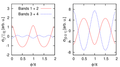
More precisely the figure shows the contributions of different bands in (4) to the two diagonal elements and of . Thereby these contributions are actually summed over pairs of bands as suggested by Figure 7, which shows that the two sheets belonging to one pair have similar Fermi surface geometry and shift in opposite direction in a magnetic field. The variation of the conductivity with field direction has the form
| (5) |
where again is the angle between magnetic field and current direction. For bands and the constant is negative and substantially larger than so that the conductivity is minimal for . This behaviour can be reproduced qualitatively already in the framework of the generic model (1). In the limit evaluation of (4) yields
| (6) |
Numerical evaluation shows that this result is quite general, i.e.
has the form (5) with and for any or
. Figure 9 shows the numerical values of versus
. Nonvanishing magnetoresistance occurs only
above a threshold value which depends on .
This was found previously by Raimondi et al.Raimondi
although these authors did not consider the detailed
variation with field direction.
The behaviour of the contribution from
bands and differs strongly from the prediction of the simple model.
First, the variation of has a substantial admixture
of the higher angular harmonic . Second, while the variation of
does have a predominant behaviour,
one now has . The deviating behaviour for this pair of bands
is hardly surprising in that Figure 7
shows that the displacement of the Fermi surface is practically
zero for but quite strong for
which suggests that for these two bands
the effective Rashba parameter depends on
the direction of the magnetic field.
Despite an extensive search we were unable to find
a set of LCAO parameters such that the
sheet resistivities (obtained by inversion of the
conductivity matrix (4)) obtained with a single,
band independent
relaxation time match the experimental vs.
curves in Figure 4. Agreement with experiment could be achieved only
by choosing a band-dependent relaxation time, more precisely
the relaxation time for the bands and had to be chosen
larger by roughly a factor as compared to for bands
and . The relaxation times obtained by fitting the experimental data
are shown in Figure 10. They have the expected
order of magnitude and their monotonic and smooth variation with magnetic field
is a few percent. Using the Fermi surface averages
of the Fermi velocity of
the mean free paths are
nm and nm.

The resulting -dependence of the sheet resistance is compared to the experimental data in Figure 11. While the agreement for current along is good, there is some discrepancy for current along in that the experimental curves have wide minima and sharp maxima, whereas this is opposite for the calculated curves.
This may indicate the limitations of the
quasiclassical Boltzmann approach as already discussed in Ref. 27
where a full solution of the Boltzmann equation was necessary to reproduce
the experimental data. For completeness
we note that a band dependent relaxation time
has been observed experimentally in materials such
as MgB2Yelland and some iron-pnictide
superconductorsTerashima2 ; Terashima .
Summarizing this section we may say that while a detailed
fit of the experimental data in the framework of the relaxation time
approximation to semiclassical Boltzmann theory is not entirely successful,
the overall behavior observed in experiment - a variation of the
conductivity with magnetic field direction
predominantly according to i.e. a
noncrystalline anisotropy, is quite generic and can be reproduced
qualitatively already in the simplest model (1). Interestingly
the considerably more complicated and
anisotropic band structure does not change this significantly.
On the other hand, the results show that the
Rashba effect in the (110) surface is strongly anisotropic so that
some deviations from this simple behaviour are not surprising.
The calculation moreover shows that at least within the framework of the
relaxation time approximation the lifetime for electrons in the
two inner Fermi surface sheets must be chosen shorter.
IV Summary
Anisotropic electronic transport of the 2DES in AO/STO was
characterized by temperature and magnetic-field dependent 4-point resistance
measurements along different crystallographic directions.
Anisotropic
behavior of is evident over the complete measured -range
(KK)
with lowest sheet resistance and largest electron mobility along the
direction. The anisotropy
of is mainly responsible for the anisotropic behavior of the normal
magnetotransport for KK, where lorentz
scattering dominates magnetotransport.
At K and T, is dominated by weak
antilocalization. The spin
orbit field deduced from WAL is well comparable to that found in (001)
AO/STO and LAO/STO and seems to depend not on specific crystallographic
direction.
Tight-binding
calculations were carried out to model the electronic subbandstructure,
confirming the anisotropy of . Despite the high anisotropy
of the Fermi surfaces, the shows a
non-crystalline behavior with
resistance maxima for in-plane magnetic field parallel to current direction.
Semi-classical Boltzmann theory was used to calculate conductivity and
confirming the rather unexpected experimental result of a non-crystalline
, despite strong anisotropic Fermi surface sheets
and Rashba coupling which however lead to
a strong sensitivity of the
behavior of AO/STO on as already observed for LAO/STO.
On the other side, electronic subband-engineering by, e. g., epitaxial strain,
may also provide possibilities to tune behavior which
might be interesting with respect to spintronics.
ACKNOWLEDGEMENTS
Part of this paper was supported by the Deutsche Forschungsgemeinschaft (DFG)
Grant No. FU 457/2-1. We are grateful to R. Thelen and the Karlsruhe Nano
Micro Facility (KNMF) for technical support. We also acknowledge D. Gerthsen
and M. Meffert from the laboratory for electron microscopy (LEM) for
transmission electron microscopy analysis of our samples.
V Appendix: LCAO calculation
We describe bulk SrTiO3 as a simple cubic lattice of Ti atoms with lattice constant unity at the positions and retain only the three orbitals of each Ti atom. The Hamiltonian is most easily formulated in a coordinate system with axes parallel to Ti-Ti bonds which we call the bulk coordinate system. In the following always refer to the bulk coordinate system, are assumed to be pairwise unequal, and denotes the lattice vector in -direction. Following Wang et al.11 we use a tight-binding parameterization of the Hamiltonian with hopping integrals
| (7) |
Following Zhong et al.Zhong
we model the interface as a hemispace of bulk SrTiO3
with surface perpendicular to the unit vector
and the origin of the
coordinate system coinciding with some atom on the surface.
Accordingly, only atoms with are retained.
The electrons are confined to the interface by a wedge-shaped
electrostatic potential which gives an extra energy
with for
all three orbitals on the Ti atom at .
The unit-cell of the resulting surface is a rectangle
with edges and .
The Brillouin zone has the extension in
-direction and in -direction and we define
and .
Using the model described so far, Wang et al.
obtained an excellent fit to their ARPES band structure at
the SrTiO3 surface by using the values
meV, meV, meV
and . Using these values, the conductivity
calculated within the Boltzmann equation formalism (as described in the
main text)
shows a rather strong anisotropy,
,
much larger than the experimental value
.
The reason is that for the low electron densities of /unit
cell in our experiment the -derived band which has small effective
mass along the direction (see Figure 5)
is almost empty. This can be changed, however,
by reducing meV for all bonds in -direction.
This reduction by might be the consequence of a slight distortion
of the lattice in the neighborhood of the interface. The same reduction
of the anisotropy could also be obtained by lowering the energy of the
-orbital by meV. Both modifications
shift the minimum of the -derived band to lower energy
and thus increase its filling.
To discuss the magnetoconductance
we extended the model of Wang et al. by including the Rashba effect -
that means the combined effect of spin-orbit coupling in the Ti 3d shell
and the confining electric field - as well as an external magnetic field.
First, the nonvanishing matrix elements
of the of orbital angular momentum operator
within the subspace of the orbitals are
plus two more equations obtained by cyclic permutations of . Choosing the basis on each Ti atom as one thus finds
where is the unit matrix in spin space. The Hamiltonian for the spin orbit-coupling then isZhong
Here denotes two more terms obtained by cyclic permutation of and is the vector of Pauli matrices. We use meV. The coupling to an external magnetic field is
with the Bohr magneton and
we use fete .
In addition to the matrix elements (7) the confining electric field
gives rise to small but nonvanishing hopping elements, which
would vanish due to symmetry in the bulk.
The respective term in the Hamiltonian is
where
is the component of the electric field perpendicular
to the bond. As shown by Zhong et al.Zhong the respective
matrix elements can be written as (, and
refer to the bulk system and are pairwise unequal)
and we used the value meV. The sign of
is positive if one really considers only
two -orbitals at the given distance. This might change if one
really considers hopping via the oxygen-ion between the two
Ti ions in the true crystal structure of SrTiO3.
We have verified, however,that inverting the sign of does not
change the angular dependence of the magnetoresistance in
Figure 11, although it does in fact
change the direction of the shift of the Fermi surface sheets in
Figure 3, that means the sign of the effective
. In fact, as can be seen from (6)
the sign of does not influence the angular variation
of the conductivity.
We neglect any matrix elements of the electric field
between orbitals centered on atoms more distant than
nearest neighbors. The interplay between these additional hopping
matrix elements and the spin orbit coupling gives rise to the
Rashba splitting of the bands.
Adding the respective terms to the tight-binding Hamiltonian
we obtain the band structure and its variation with a magnetic field.
We have verified that slight variations of ,
or do not lead to qualitative changes of the results reported in the
main text.
References
- (1) N. Reyren, S. Thiel, A. D. Caviglia, L. FG. Hammerl, C. Richter, C. W. Schneider, T. Kopp, A. S. Ruetschi, D. Jaccard, M. Gabay, D. A. Muller, J.M. Triscone, and J. Mannhart, Science 317, 1196 (2007).
- (2) A. D. Caviglia, M. Gabay, S. Gariglio, N. Reyren, C. Cancellieri, and J. M. Triscone, Phys. Rev. Lett. 104, 126803 (2010).
- (3) J. Biscaras, N. Bergeal, S. Hurand, C. Feuillet-Palma, A. Rastogi, R. C. Budhani, M. Grilli, S. Caprara, and J. Lesueur, Nature Mater. 12, 542 (2013).
- (4) A. Brinkman, M. Huijben, M. Van Zalk, J. Huijben, U. Zeitler, J. C. Maan, W. G. Van der Wiel, G. Rijnders, D. H. A. Blank, and H. Hilgenkamp, Nature Mater. 6, 493 (2007).
- (5) A. Joshua, S. Pecker, J. Ruhman, E. Altman, and S. Ilani, Nat. Comm. 3, 1129 (2012).
- (6) A. Fête, S. Gariglio, A. D. Caviglia, J. M. Triscone, and M. Gabay, Phys. Rev. B 86, 201105(R) (2012).
- (7) A. Joshua, J. Ruhman, S. Pecker, E. Altman, and S. Ilani, Proc. Natl. Acad. Sci. U. S. A. 110, 9633 (2013).
- (8) H. J. Harsan Ma, J. Zhou, M. Yang, Y. Liu, S. W. Zeng, W. X. Zhou, L. C. Zhang, T. Venkatesan, Y. P. Feng, and Ariando, Phys. Rev. B 95, 155314 (2017).
- (9) M. Trushin, K. Výborný, P. Moraczewski, A. A. Kovalev, J. Schliemann, and T. Jungwirth, Phys. Rev. B 80, 134405 (2009).
- (10) Y.Z. Chen, N. Pryds, J. E. Kleibeuker, G. Koster, J. Sun, E. Stamate, B. Shen, G. Rijnders, and S. Linderoth, Nano Lett. 11, 3774 (2011).
- (11) Z. Wang, Z. Zhong, X. Hao, S. Gerhold, B. Stöger, M. Schmid, J. Sanchez-Barriga, A. Varykhalov, C. Franchini, K. Held, and U. Diebold, Proc. Natl. Acad. Sci. U. S. A. 111, 3933 (2014).
- (12) D. Fuchs, R. Schäfer, A. Sleem, R. Schneider, R. Thelen, and H. v. Löhneysen, Appl. Phys. Lett. 105, 092602 (2014).
- (13) D. Fuchs, K. Wolff, R. Schäfer, R. Thelen, M. Le Tacon, and R. Schneider, AIP Advances 7, 056410 (2017).
- (14) M. Huijben, G. Rijnders, D. H. A. Blank, S. Bals, S. V. Aert, J. Verbeeck, G. V. Tendeloo, A. Brinkman, and H. Hilgenkamp, Nat. Mater. 5, 556 (2006).
- (15) Y. Li, Y. Lei, B. G. Shen, and J. R. Sun, Sci. Rep. 5, 14576 (2015).
- (16) K. Gopinadhan, A. Annadi, Y. Kim, A. Srivastava, B. Kumar, J. Chen, J. M. D. Coey, Ariando, and T. Venkatesan, Adv. Electron. Mater. 1, 1500114 (2015).
- (17) S.-C. Shen, Y.-P. Hong, C.-J Li, H.-X. Xue, X.-X. Wang, and J.-C. Nie, Chin. Phys. B 7, 076802 (2016).
- (18) D. van der Marel, J. L. M. van Mechelen, and I. I. Mazin, Phys. Rev. B 84, 205111 (2011).
- (19) D. Fuchs, A. Sleem, R. Schäfer, A. G. Zaitsev, M. Meffert, D. Gerthsen, R. Schneider, and H. v. Löhneysen, Phys. Rev. B 92, 155313 (2015).
- (20) K. Wolff, R. Schäfer, M. Meffert, D. Gerthsen, R. Schneider, and D. Fuchs, Phys. Rev. B 95, 245132 (2017).
- (21) A. Othomo and H. Y. Hwang, Nature 427, 423 (2004).
- (22) G. Herranz, F. Sánchez, N. Dix, M. Scigaj, and J. Fontcuberta, Sci. Rep. 2, 758 (2012).
- (23) P. A. Lee and T. V. Ramakrishnan, Rev. Mod. Phys. 57, 287 (1985).
- (24) S. Maekawa and H. Fukuyama, J. Phys. Soc. Jpn. 50, 2516 (1981).
- (25) A. P. Pippard, Magnetoresistance in Metals (Cambridge University Press, Cambridge, 1998).
- (26) M. Diez, A. M. R. V. L. Monteiro, G. Mattoni, E. Cobanera, T. Hyart, E. Mulazimoglu, N. Bovenzi, C. W. J. Beenakker, and A. D. Caviglia, Phys. Rev. Lett. 115, 016803 (2015).
- (27) Z. Zhong, A. Toth, and K. Held, Phys. Rev. B 87, 161102(R) (2013).
- (28) R. Raimondi, M. Leadbeater, P. Schwab, E. Caroti, and C. Castellani, Phys. Rev. B 64, 235110 (2001).
- (29) E. A. Yelland, J. R. Cooper, A. Carrington, N. E. Hussey, P. J. Meeson, S. Lee, A. Yamamoto, and S. Tajima, Phys. Rev. Lett. 88, 217002 (2002)
- (30) T. Terashima, N. Kurita, M. Tomita, K. Kihou, C.-H. Lee, Y. Tomioka, T. Ito, A. Iyo, H. Eisaki, T. Liang, M. Nakajima, S. Ishida, S.-I. Uchida, H. Harima, and S. Uji, Phys. Rev. Lett. 107, 176402 (2011)
- (31) T. Terashima, N. Kurita, M. Kimata, M. Tomita, S. Tsuchiya, M. Imai, A. Sato, K. Kihou, C.-H. Lee, H. Kito, H. Eisaki, A. Iyo, T. Saito, H. Fukazawa, Y. Kohori, H. Harima, and S. Uji, Phys. Rev. B 87, 224512 (2013).
- (32) A. Fête, S. Gariglio, C. Berthod, D. Li, D. Stornaiuolo, M. Gabay, and J.-M. Triscone, New J. Phys. 16, 112002 (2014).