Room temperature deposition of superconducting Niobium Nitride films by ion beam assisted sputtering
Abstract
We use room temperature ion beam assisted sputtering (IBAS) to deposit niobium nitride thin films. Electrical and structural characterizations were performed by electric transport and magnetization measurements at variable temperatures, X-ray diffraction and atomic force microscopy. Compared to reactive sputtering of NbN, films sputtered in presence of an ion beam show remarkable increase in the superconducting critical temperature Tc, while exhibiting lower sensitivity to nitrogen concentration during deposition. Thickness dependence of the superconducting critical temperature is comparable to films prepared by conventional methods at high substrate temperatures and is consistent with behavior driven by quantum size effects or weak localization.
I Introduction
Niobium nitride (NbN) has long been a material of interest for fabrication of nano-devices in the field of quantum electronics, such as superconducting nanowire single photon detectorsGol’tsman et al. (2001) and superconducting SIS tunnel junctionsKawakami et al. (2001) due to its relatively high superconducting Tc, large superconducting energy gap and ease of fabrication. However, one of the undesired features of NbN is the presence of multiple crystal structure modifications, not all of them superconducting.Oya and Onodera (1974) Conventional fabrication methods, such as reactive sputteringShoji et al. (1992) or CVD and thermal diffusionGurvitch et al. (1985), stabilize the growth of a desired phase of NbN by carrying out the deposition at elevated temperatures, generally more than 500 ∘C, which makes the process incompatible with methods like lift-off, heterostructure growth with materials sensitive to heat or fabrication of tunnel junctions, where impurity diffusion leads to interaction at the junction interface. Recently the superconductivity with high critical temperature in hard -NbN grown at high pressure and high temperatures was discovered.Zou et al. (2016) While there exist processes capable of achieving high-Tc NbN films deposited at room temperature, such as incorporation of methane gas with RF diode sputteringCukauskas (1983), they lead to films with a granular or columnar void structure, resulting in normal state resistivity well above 104 Cukauskas (1983); Kawakami et al. (2001). Use of substrate biasing during deposition procedure has also been demonstrated to be a viable method of room temperature deposition, but deposited films show presence of lower-Tc tetragonal phase of NbN, which leads to suppression of overall film critical temperature.Dane et al. (2017) These growth methods require extremely precise control over relative concentrations of sputtering gasses and large sputtering powers, which leads to substrate heating.Bacon et al. (1983)
Use of ion beam bombardment during deposition process is known to have dramatic impact on the microstructure of films.Smidt (1989); Harper et al. (1984) It leads to densification of films and increases adhesionHirsch and Varga (1980) and the additional kinetic energy supplied by the ion beam allows for increased mobility of the atomic species near the surface, reducing the presence of voids that are substituted by dislocation boundariesHibbs et al. (1984); Marchenko and Neklyudov (2008). Also, the increase in the momentum anisotropy leads to development of texture with preferred orientation of film grainsMüller (1985); Dobrev (1982); Van Wyk and Smith (1980); Ma et al. (2004). In this work we explore ion beam assisted sputtering (IBAS) that combines N2 bombardment with conventional DC magnetron sputtering. We show that IBAS can be used to produce NbN thin films with superior superconducting properties even with deposition carried out with substrate at room temperatures. We demonstrate that use of neutralized nitrogen ion beam during DC magnetron sputtering from a Nb target leads to NbN films with relatively high superconducting transition temperatures of up to 14.5 K and with normal resistivity as low as 110.62 , without any need for substrate heating or biasing. A direct comparison of IBAS to conventional DC reactive sputtering carried out in the same chamber shows not only an increase in superconducting critical temperature Tc of NbN films, but also a large decrease in process sensitivity to nitrogen concentration, leading to more consistent results compatible with large scale fabrication. We conduct structural and electrical characterization of the IBAS-grown non-epitaxial thin NbN films focusing on the mechanism of suppression of superconductivity in very thin films grown on Si wafers. We find that thin films grown by IBAS have good superconducting properties down to a critical thickness of approximately 2 nm, which is comparable to films grown by conventional methods on epitaxial substrates at high temperatures. We demonstrate that the evolution of superconducting transition temperature with film thickness T can be explained by quantum size effects or, potentially, weak localization.
II Sample Fabrication Methods
NbN films were prepared by DC magnetron sputtering in a commercial ultra-high vacuum sputtering system (Angstrom Engineering).Ang After transferring the silicon wafer substrate with thermally grown silicon oxide through a load-lock, the chamber was pumped down to less than 10-8 Torr before commencing the deposition procedure. Before the actual sputtering step, the substrate’s surface was treated using a low energy argon ion beam. This is done primarily to eliminate any water or organic contamination and without loss of more than 1 nm of the substrate surface.
Sputtering was carried out at 2 mTorr with Ar2 (99.9999% purity) as sputtering gas. During reactive sputtering, N2 (99.9997% purity) gas was mixed into the sputtering gas, while in ion beam assisted sputtering, nitrogen was supplied through the ion gun only. The amount of argon and nitrogen was controlled by mass flow controllers and monitoring of residual and sputtering gasses was done by a quadrupole gas analyzer, to ensure equivalent gas mixture in the chamber for comparison of reactive and ion beam assisted sputtering.
The 3 in dia. sputtering target consisted of 99.9999% pure Nb, it was located 5 in. away from the substrate at a 33∘ angle relative to substrate surface normal and powered at 0.18 kW from a DC magnetron power source. Sputtering rates of approximately 1 Å/s were determined from a calibrated quartz thickness monitor and confirmed after deposition by X-Ray reflectometry or by profilometer measurement on a shadowmasked twin sample. A slight difference in sputtering rates is observed when compared to reactive sputtering, which is approximately 15% lower under equivalent conditions.
The ion beam source was an End-Hall ion gunKaufman et al. (1987), in which neutralization of nitrogen ions was achieved by thermionic emission of electrons from a hollow cathode. The ion gun, positioned at azimuthal 20∘ relative to the sputtering gun and at an angle of 40∘ relative to sample surface normal, was operated in constant gas flow mode, to facilitate comparison with reactive sputtering, while discharge and emission currents and voltages were kept constant during deposition. As ion bombardment at energies above 300 eV are known to cause structural damage to thin filmsKern (2012), the energy of the ion beam was kept at relatively low value of 100 eV per N2 in order to minimize these effects. This translates to ion beam power densities of approximately 70 mW/cm2. Total ion beam current under these conditions was maintained at nominal 0.5 A. The value of 100 eV per N2 was deemed optimal based on comparison with depositions carried out at 50, 200 and 300 eV, which lead to maximum Tc of 12.9, 13.6 and 13.1 K, respectively. The reduction of Tc at lower energies can be explained by decrease in mobility of adatoms and defects due to reduction of available kinetic energy from the incoming ions.
The films were grown on polished Si substrates with native oxide without any intentional heating during deposition. Self-heating due to sputtering did not exceed 55∘C, as determined by a calibrated thermocouple built into the substrate holder assembly.
III Results and Discussion
III.1 Characterization of thick NbN films
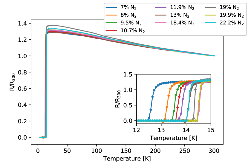
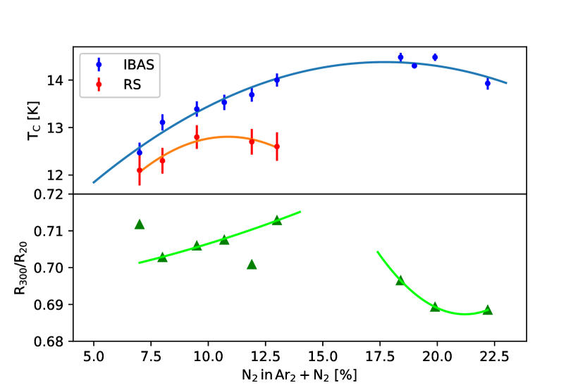
The superconducting and residual resistivity ratio were measured using the standard four probe technique in a Quantum Design PPMS. Resistive transitions of 240 nm thick NbN films deposited on Si substrate by IBAS can be seen Fig. 1. To better demonstrate the dependence of superconducting on the concentration of nitrogen and to facilitate comparison to reactive sputtering, the superconducting transition temperatures are explicitly plotted as a function of nitrogen concentration in Fig. 2, with the general trend of both curves that follows results in literatureKawakami et al. (2001); Oya and Onodera (1974); Shoji et al. (1992); Cukauskas (1983); Bacon et al. (1983): the superconducting peaks and the transition width shrinks as the NbN film approaches optimal stoichiometry. However, one can clearly see a quantitative difference when comparing the two techniques. First, there is a significant difference in the highest value of the superconducting , with the IBAS samples reaching 14.5 K, close to optimum value for bulk stoichiometric NbN. Second, there is obvious decrease in the process sensitivity towards the concentration of nitrogen in the growth chamber: one can achieve 14 K in a range of concentrations from 13% to 22% - a dramatic improvement from reactive sputtering, in which high superconducting Tc is constrained to a window of approximately 2%.Kawakami et al. (2001) Room-temperature resistivity of the thin films was 110.66.6 , showing no noticeable trend with N2 concentration.
We confirmed close to optimal stoichiometry for the phase with the highest Tc using X-ray diffraction (Fig. 3). We observe prominent peaks of the cubic -NbN, without any presence of the non-superconducting phases, such as the common -NbN phase.Benkahoul et al. (2004)
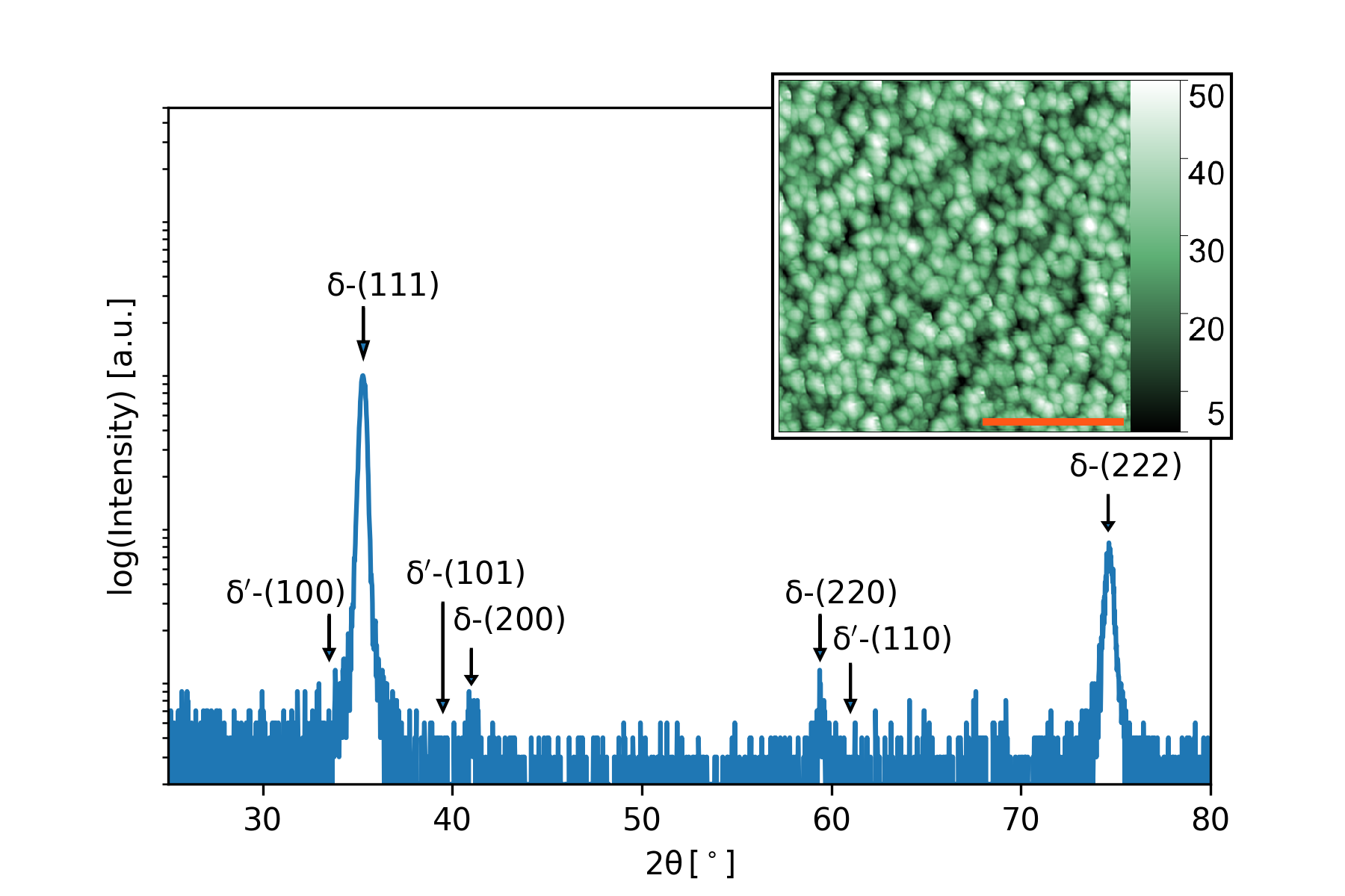
Despite the results indicating textured films containing predominantly cubic -NbN phase, the superconducting Tc of the films is lower than that of single crystal NbN. This could be explained by effects of grain boundaries suppressing the local density of states, leading to reduced total Tc, even if the intragrain Tc would be close to maximum.Tyan and Lue (1994); Nigro et al. (1988) This effect was observed in some of our magnetization measurements, where the superconducting transition has a long tail of more than 1 Kelvin. This is further corroborated by the residual resistivity ratios RRR = , which are all smaller than unity, an effect attributed to grain boundary scattering of conduction electrons.Tyan and Lue (1994) Consistently with this description, the RRR correlates with the superconducting Tc, reaching a maximum value of approximately 0.72 (Fig. 2). By correlating this value with findings in literature, this RRR corresponds to average grain size of approximately 25 nmNigro et al. (1988), in agreement with values we have determined by XRD (22 nm) and AFM (mean grain width of 25 5 nm) measurements. Additionally, the limited presence of voids in films deposited by IBAS might come at the expense of increased density of dislocation defectsMarchenko and Neklyudov (2008). This micro-structural disorder can cause additional electron scattering, increasing the film resistance, decreasing the RRR and also potentially lead to weak localization as discussed in the next section.
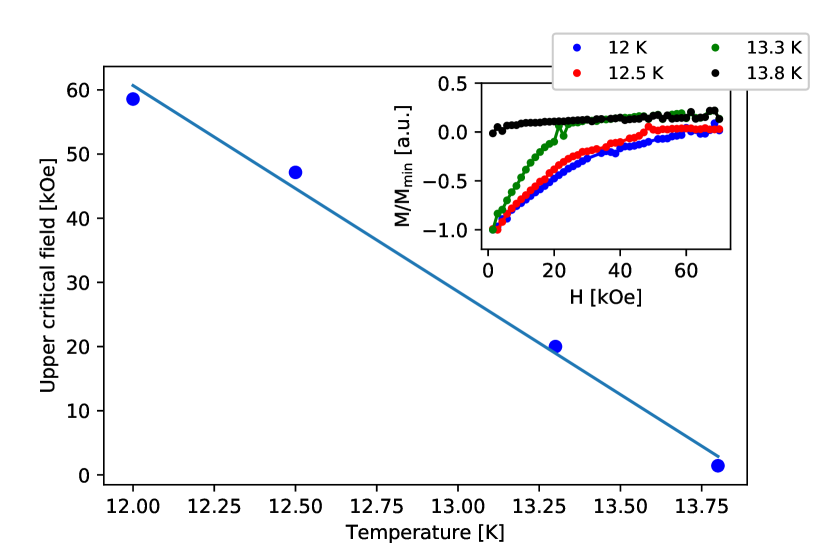
To determine upper critical magnetic field and coherence length, we carried out magnetization measurements at various fields close to superconducting Tc, where the temperature dependent Hc2(T) was defined as a field at which the magnetization vanishes. The upper critical field Hc2(T=0 K) was calculated by extrapolation from the Werthamer-Helfand-Hohenberg formulaWerthamer et al. (1966):
| (1) |
The in-plane coherence length was obtained from the Ginzburg-Landau theory, where Tinkham (1996):
| (2) |
Strictly speaking, this dependence should be valid only in the critical region close to superconducting Tc, but in practice, it can be applied even deep into the superconducting state. From the upper critical fields measured for film grown at optimal conditions (Fig. 4), the extrapolated perpendicular critical field was determined to be Hc2(0) = 319 kOe and the estimated coherence length is = 3.2 nm, slightly smaller than the bulk value of 5 nm reported in literatureJha et al. (2012); Vasyutin et al. (2016). This reduced value of is the result of the renormalization of coherence length due to short electron mean-free path in disordered sputtered films.Faucher et al. (2002)
III.2 Suppression of superconductivity in ultra-thin films
As many applications of superconducting devices necessitate for the material to be in a form of a thin film, we also study the dependence of superconducting and electronic properties as a function of film thickness. It is well known that in NbN the superconducting state is suppressed as the film becomes thin,Il’in et al. (2004); Engel et al. (2006); Semenov et al. (2009) and it is usually explained either by weak localizationGraybeal and Beasley (1984); Xiao and Chien (1996); Kim et al. (2006), electron wave leakageYu et al. (1976) or surface contribution to the Ginzburg-Landau free energy of the superconductor.Simonin (1986)
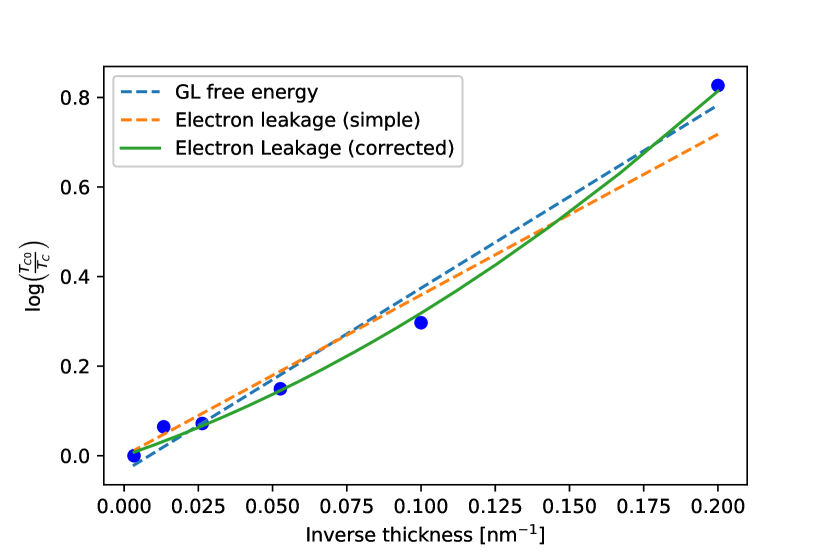
One way to determine which model best fits our experimental data is to look at the dependence of the superconducting Tc on film thickness (Fig. 5). In electron leakage model, the the electron wave function is considered to be quantized in the direction perpendicular to sample surface. This quantization leads to reduction in density of states and allows for the wave function to leak outside of the superconductor. The simplified theory predicts a behavior of superconducting Tc asYu et al. (1976); Kang et al. (2011):
| (3) |
where is the critical temperature of bulk, is the characteristic length of electron wave leakage, approximately equal to the electron Fermi wavelength, and is the BCS coupling. If we assume = 0.32Kang et al. (2011), the estimated = 1.14 Å is reasonably close to the reported values for NbN. However, considering the disordered nature of sputtered films, one might want to use a version of Eq. (3) corrected for presence of defects and film breakup:
| (4) |
where is a term describing contribution of defects and is typically in the range from 0 to 20 Å2. Usage of parameters reported on previous films Kang et al. (2011) leads to quantitative behavior similar to the uncorrected theory. Removing this restriction allows for a quantitatively better fit, with estimated values = 0.73 Å and = 2.84 Å2. The length of is not significantly shorter than the reported values and falls within expected range, meaning that the estimate is not unphysical. The difference from values reported by Kang et. al might be explained by difference in the microstructure of our films, as evidenced by different sheet resistance of thin films produced by our IBAS method.
Considering the approximately linear trend of superconducting T, a variational result from modified Ginzburg-Landau theory with an added surface term could also be appliedSimonin (1986):
| (5) |
where is the Thomas-Fermi screening length. Using this model, we can extrapolate the limiting thickness where the superconducting state vanishes as , which is comparable to the coherence length extracted from Eq. (2) and supports the notion that ion beam assisted sputtering achieves growth without considerable amount of non-superconducting interfacial layers, even on substrates with considerable lattice mismatch. Further, we can estimate the value of screening length , in good agreement with the assumption of it being on the order of lattice spacingChockalingam et al. (2009); Piatti et al. (2016) and much smaller than the coherence length .
More insight into the behavior of the superconducting state in thin films can be gained from the dependence of Tc on the films’ sheet resistance Rsheet. Ivry et. al. proposed a phenomenological power-law dependence of the formIvry et al. (2014):
| (6) |
where is the film thickness and and are fitting constants. This equation can be rewritten into a form:
| (7) |
which can be contrasted to the result derived from BCS theoryMcMillan (1968):
| (8) |
where is the Debye temeparture, is the electron-phonon coupling constant and describes Coulomb repulsive interactions. When comparing equations (7) and (8), one can see that the term is related to changes in the BCS coupling (in weak coupling limit equal to ) or the interaction parameters and , which would scale as . Fitting our experimental data to equation (6) yields a result , different from the average value of (although still within range of reported valuesIvry et al. (2014)).
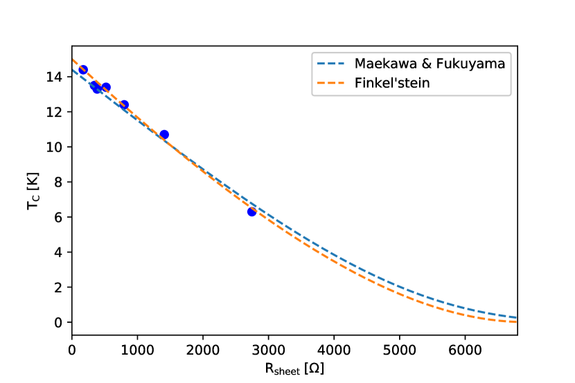
A more quantitative approach to study of Coulomb interactions and localization effects can be also applied. Perturbation theory for localization in 2D superconductors, developed by Maekawa and Fukuyama, yields a result for superconducting Tc in the formMaekawa and Fukuyama (1982):
| (9) |
where is the coherence length, is the electronic mean free path and is an effective BCS coupling constant. In the dirty limit of , the first term, which is due to reduction of density of states, becomes negligible when compared to the second term, corresponding to a vertex correction to the electron-electron interaction. Under these assumptions, the superconducting Tc reduction should have an approximately linear dependence on the film sheet resistance. While our results do show linear behavior (as seen in Fig. 6), a fit to Eq. (9) provides the effective BCS coupling constant N(0) = 23.62, which is an unphysically large correction to the standard BCS value of 0.32. Also, a superconductor to insulator transition can typically be driven by weak localization when the sheet resistances are around the quantum value 6.4 Kagawa et al. (1996), as can be seen also when extending our fit. Extrapolating the dependence of Rsheet vs film thickness, the critical thickness for this transition is approximately 2 nm, which is close to the estimate from Eq. (5). Alternatively, one can employ Finkel’stein’s results using renormalization group methodsFinkel’stein (1996); *finkelstein_jetplett1987; *finkelstein_physicab_1994:
| (10) |
where , , kB is the Boltzmann constant, is the elementary charge and is the electron elastic scattering time. Fitting our data to this equation yields = 2.43 s, four times smaller than the value reported in literatureEzaki et al. (2012). This difference is not surprising when one considers higher resistance of our thin films and its relation to the electronic mean-free path, which is proportional to .
Both equations (9) and (10) predict vanishing superconductivity at values of Rsheet that coincide with critical thicknesses extrapolated from models related to dimensionality effects (equations (3), (4) and (5)), which complicates determination of suppression mechanism. Multiple results in literature observe critical thickness for NbN close to 2 nm in films prepared using different growth conditions and therefore having different electronic propertiesSemenov et al. (2009); Kang et al. (2011); Wang et al. (1996); Ezaki et al. (2012); Makise et al. (2015); Ivry et al. (2014), which might be an indication that the reduction of superconducting Tc is driven by effects related to dimensionality. However, there has been no observation of higher order effects, such as Tc oscillation with thickness predicted by the electron leakage model, in this work or others. As Eq. (10) yields a good quantitative fit with physically reasonable values, further study is required to rule out localization effects as a mechanism for suppression of Tc, even more so, when one considers the disordered nature of sputtered films.
IV Conclusions
We have shown that NbN thin film growth using low energy bombardment with N2 during sputtering of Nb has beneficial effects on superconducting and electronic properties of the resulting NbN films. This room temperature process results in films having resistivity as low as 110 .cm, relatively high Tc of 14.5 K and critical magnetic field of nearly 32 T. The stoichiometric growth can be achieved in a broad range of nitrogen concentrations and does not require epitaxial growth conditions, which opens opportunities for broader application of NbN in quantum electronic devices.
Our data on ultrathin NbN films supports the predictions of models of electron wave leakage (quantum size effect) or weak localization. Even on non-epitaxial substrates, superconductivity persists down to thickness of approximately 2 nm, which also coincides with sheet resistances equal to resistance quantum, where one can potentially expect superconductor-insulator transition driven by weak localization.
V Acknowgledments
The authors would like to thank Aaron Miller from Quantum Opus, LLC in Novi, MI USA and André Anders from Leibniz Institute of Surface Engineering in Leipzig, Germany for stimulating discussion.
This work was supported by the U. S. Department of Energy (DOE), Office of Science, Offices of Nuclear Physics, Basic Energy Sciences, Materials Sciences and Engineering Division under Contract # DE-AC02-06CH11357. G.K. was supported by the Center for the Computational Design of Functional Layered Materials (CCDM), an Energy Frontier Research Center funded by the U.S. Department of Energy, Office of Science, Basic Energy Sciences under Award # DE-SC0012575.
References
- Gol’tsman et al. (2001) G. Gol’tsman, O. Okunev, G. Chulkova, A. Lipatov, A. Semenov, K. Smirnov, B. Voronov, A. Dzardanov, C. Williams, and R. Sobolewski, Applied physics letters 79, 705 (2001).
- Kawakami et al. (2001) A. Kawakami, Z. Wang, and S. Miki, Journal of Applied Physics 90, 4796 (2001).
- Oya and Onodera (1974) G.-I. Oya and Y. Onodera, Journal of Applied Physics 45, 1389 (1974).
- Shoji et al. (1992) A. Shoji, S. Kiryu, and S. Kohjiro, Applied Physics Letters 60, 1624 (1992).
- Gurvitch et al. (1985) M. Gurvitch, J. Remeika, J. Rowell, J. Geerk, and W. Lowe, IEEE Transactions on Magnetics 21, 509 (1985).
- Zou et al. (2016) Y. Zou, X. Qi, C. Zhang, S. Ma, W. Zhang, Y. Li, T. Chen, X. Wang, Z. Chen, D. Welch, P. Zhu, B. Liu, Q. Li, T. Cui, and B. Li, Scientific Reports 6 (2016), 10.1038/srep22330.
- Cukauskas (1983) E. Cukauskas, Journal of Applied Physics 54, 1013 (1983).
- Dane et al. (2017) A. E. Dane, A. N. McCaughan, D. Zhu, Q. Zhao, C.-S. Kim, N. Calandri, A. Agarwal, F. Bellei, and K. K. Berggren, Applied Physics Letters 111, 122601 (2017).
- Bacon et al. (1983) D. Bacon, A. English, S. Nakahara, F. Peters, H. Schreiber, W. Sinclair, and R. Van Dover, Journal of applied physics 54, 6509 (1983).
- Smidt (1989) F. Smidt, in Structure-Property Relationships in Surface-Modified Ceramics (Springer, 1989) pp. 417–454.
- Harper et al. (1984) J. M. Harper, J. J. Cuomo, R. J. Gambino, H. R. Kaufman, O. Auciello, and R. Kelly, Auciello and R. Kelly, eds., Elsevier Science Pub. BV, Amsterdam (1984).
- Hirsch and Varga (1980) E. Hirsch and I. Varga, Thin Solid Films 69, 99 (1980).
- Hibbs et al. (1984) M. Hibbs, B. Johansson, J.-E. Sundgren, and U. Helmersson, Thin Solid Films 122, 115 (1984).
- Marchenko and Neklyudov (2008) I. Marchenko and I. Neklyudov, in Journal of Physics: Conference Series, Vol. 113 (IOP Publishing, 2008) p. 012014.
- Müller (1985) K.-H. Müller, Journal of applied physics 58, 2573 (1985).
- Dobrev (1982) D. Dobrev, Thin Solid Films 92, 41 (1982).
- Van Wyk and Smith (1980) G. Van Wyk and H. Smith, Nuclear Instruments and Methods 170, 433 (1980).
- Ma et al. (2004) C.-H. Ma, J.-H. Huang, and H. Chen, Thin Solid Films 446, 184 (2004).
- (19) https://angstromengineering.com/products/evovac/.
- Kaufman et al. (1987) H. R. Kaufman, R. S. Robinson, and R. I. Seddon, Journal of Vacuum Science & Technology A: Vacuum, Surfaces, and Films 5, 2081 (1987).
- Kern (2012) W. Kern, Thin film processes II, Vol. 2 (Academic press, 2012).
- Benkahoul et al. (2004) M. Benkahoul, E. Martinez, A. Karimi, R. Sanjinés, and F. Lévy, Surface and Coatings Technology 180, 178 (2004).
- Tyan and Lue (1994) J.-H. Tyan and J. T. Lue, Journal of Applied Physics 75, 325 (1994).
- Nigro et al. (1988) A. Nigro, G. Nobile, M. Rubino, and R. Vaglio, Physical Review B 37, 3970 (1988).
- Werthamer et al. (1966) N. Werthamer, E. Helfand, and P. Hohenberg, Physical Review 147, 295 (1966).
- Tinkham (1996) M. Tinkham, Introduction to superconductivity (Courier Corporation, 1996).
- Jha et al. (2012) R. Jha, A. Kumar, and V. Awana, in AIP Conference Proceedings, Vol. 1447 (AIP, 2012) pp. 867–868.
- Vasyutin et al. (2016) M. Vasyutin, N. Kuz’michev, and D. Shilkin, Physics of the Solid State 58, 236 (2016).
- Faucher et al. (2002) M. Faucher, T. Fournier, B. Pannetier, C. Thirion, W. Wernsdorfer, J. Villegier, and V. Bouchiat, Physica C: Superconductivity 368, 211 (2002).
- Il’in et al. (2004) K. Il’in, M. Siegel, A. Semenov, A. Engel, and H. Hübers, in Proceedings of the 6th European Conference on Applied Superconductivity (EUCAS 2003), 181 (2004) pp. 2895–2901.
- Engel et al. (2006) A. Engel, A. Semenov, H.-W. Hübers, K. Il’in, and M. Siegel, “Electric noise and local photon-induced nonequilibrium states in a current-carrying nanostructured superconductor,” (2006).
- Semenov et al. (2009) A. Semenov, B. Günther, U. Böttger, H.-W. Hübers, H. Bartolf, A. Engel, A. Schilling, K. Ilin, M. Siegel, R. Schneider, et al., Physical Review B 80, 054510 (2009).
- Graybeal and Beasley (1984) J. Graybeal and M. Beasley, Physical Review B 29, 4167 (1984).
- Xiao and Chien (1996) J. Q. Xiao and C. Chien, Physical review letters 76, 1727 (1996).
- Kim et al. (2006) K. Kim, J. H. Kwon, J. Kim, K. Char, H. Doh, and H.-Y. Choi, Physical Review B 74, 174503 (2006).
- Yu et al. (1976) M. Yu, M. Strongin, and A. Paskin, Physical Review B 14, 996 (1976).
- Simonin (1986) J. Simonin, Physical Review B 33, 7830 (1986).
- Kang et al. (2011) L. Kang, B. Jin, X. Liu, X. Jia, J. Chen, Z. Ji, W. Xu, P. Wu, S. Mi, A. Pimenov, et al., Journal of Applied Physics 109, 033908 (2011).
- Chockalingam et al. (2009) S. Chockalingam, M. Chand, A. Kamlapure, J. Jesudasan, A. Mishra, V. Tripathi, and P. Raychaudhuri, Physical Review B 79, 094509 (2009).
- Piatti et al. (2016) E. Piatti, A. Sola, D. Daghero, G. Ummarino, F. Laviano, J. R. Nair, C. Gerbaldi, R. Cristiano, A. Casaburi, and R. Gonnelli, Journal of Superconductivity and Novel Magnetism 29, 587 (2016).
- Ivry et al. (2014) Y. Ivry, C.-S. Kim, A. E. Dane, D. De Fazio, A. N. McCaughan, K. A. Sunter, Q. Zhao, and K. K. Berggren, Physical Review B 90, 214515 (2014).
- McMillan (1968) W. McMillan, Physical Review 167, 331 (1968).
- Maekawa and Fukuyama (1982) S. Maekawa and H. Fukuyama, Journal of the Physical Society of Japan 51, 1380 (1982).
- Kagawa et al. (1996) K. Kagawa, K. Inagaki, and S. Tanda, Physical Review B 53, R2979 (1996).
- Finkel’stein (1996) A. Finkel’stein, in 30 Years Of The Landau Institute - Selected Papers (World Scientific, 1996) pp. 288–291.
- Finkel’stein (1987) A. Finkel’stein, Sov. Phys. JETP Lett. 45, 46 (1987).
- Finkel’stein (1994) A. Finkel’stein, Physica B: Condensed Matter 197, 636 (1994).
- Ezaki et al. (2012) S. Ezaki, K. Makise, B. Shinozaki, T. Odo, T. Asano, H. Terai, T. Yamashita, S. Miki, and Z. Wang, Journal of Physics: Condensed Matter 24, 475702 (2012).
- Wang et al. (1996) Z. Wang, A. Kawakami, Y. Uzawa, and B. Komiyama, Journal of applied physics 79, 7837 (1996).
- Makise et al. (2015) K. Makise, T. Odou, S. Ezaki, T. Asano, and B. Shinozaki, Materials Research Express 2, 106001 (2015).