Epitaxial UN and -U2N3 Thin Films
Abstract
Single crystal epitaxial thin films of UN and U2N3 have been grown for the first time by reactive DC magnetron sputtering. These films provide ideal samples for fundamental research into the potential accident tolerant fuel, UN, and U2N3, its intermediate oxidation product. Films were characterised using x-ray diffraction (XRD) and x-ray photoelectron spectroscopy (XPS), with XRD analysis showing both thin films to be [001] oriented and composed of a single domain. The specular lattice parameters of the UN and U2N3 films were found to be 4.895 Å and 10.72 Å, respectively, with the UN film having a miscut of 2.6 ∘. XPS showed significant differences in the N-1s peak between the two films, with area analysis showing both films to be stoichiometric.
I Introduction
Uranium mononitride, UN, is of significant interest to the nuclear industry due to its high melting point, high uranium density, and improved thermal conductivity in comparison to uranium dioxide, UO2 Kurosaki et al. (2000). In addition to the enhanced thermal conductivity, providing an improved accident response, the 40 % higher uranium density of UN allows for lower enrichment or higher fuel burn-up Terrani et al. (2014). Despite these known advantages, there are still many material properties of UN yet to be fully investigated, in particular, there are concerns over the rapid oxidation of UN in water Dell et al. (1967); Sugihara and Imoto (1969); Jolkkonen et al. (2017). This oxidation reaction has been shown to progress with the formation of a U2N3 interlayer between UN and UO2, making it also of interest Paljević and Despotović (1975); Rao et al. (1991). A better understanding of this oxidation process, as well as fundamental fuel properties, such as thermal conductivity and irradiation performance, is required for UN to be considered as a viable accident tolerant fuel (ATF). Consequently, this area of research has had a renewal of interest, with several recent experiments utilising thin film samples Long et al. (2016); Wang et al. (2016); Lu et al. (2016).
Thin films provide an ideal way to research these properties, with their enhanced surface sensitivity being optimal for investigating surface reactions such as oxidation and hydrolysis, and ability to produce highly controlled samples, allowing for single variable investigations. These experiments improve fundamental understanding of materials and provide experimental data comparable to theoretical calculations which are of particular importance in an area of research that is restricted as a result of radioactivity. In addition, thin films contain such little radioactive material that they do not require dedicated facilities and are more likely to be classed as exempt from radioactive material transport regulations.
Polycrystalline UN and U2N3 films have previously been grown by reactive DC magnetron sputtering and epitaxial thin films of UN2 have been grown by polymer assisted deposition Black et al. (2001); Long et al. (2016); Scott et al. (2014). However, prior to this study there have been no reports on the successful deposition of epitaxial UN and U2N3 films. It is noted that while the fabrication of bulk single crystal UN is documented, there have been no prior reports of single crystal U2N3 Curry (1965). The ability to grow epitaxial UN and U2N3 thin films will therefore contribute to the advancement of ATF research, providing idealised samples on which to conduct fundamental material behaviour studies.
II Experimental Details
The films were grown in a DC magnetron sputtering system at the University of Bristol with 10-8 mbar base pressure, in-situ reflection high-energy electron-diffraction (RHEED), and substrate heating to 1200 ∘C, with the temperature at the substrate position calibrated using a pyrometer. The system uses 5.5N argon at 7x10⁻³ mbar as the main sputtering gas, and houses a target of depleted uranium, producing deposition rates in the range of 0.5-1.5 Å/s.
A partial pressure of 5.5N N2 is used to reactively deposit nitride films, with the pressure determining the phase deposited, as shown by Black Black et al. (2001). Polycrystalline samples were grown at room temperature to optimise the N2 partial pressure required to deposit single phase films of UN and U2N3, 2.0x10⁻⁵ mbar and 9.0x10⁻⁴ mbar, respectively, similar to that of Black
In order to grow single crystal films, compatible substrates with epitaxial matches were chosen and heated during deposition. Substrates that did not contain oxygen were sought to prevent oxidation of the deposited nitride. The substrates used were 10 mm x 10 mm, supplied by MTI corporation, single sided polished to 1-3 Å root mean square (RMS) roughness and mechanically mounted onto sample holders.
Cubic \hkl[001] CaF2 was used as the substrate to epitaxially deposit U2N3 in the \hkl[001] direction at 700 ∘C. It was selected as its bulk lattice parameter of 5.463 Å has only a 2.3 % mismatch with bulk -U2N3, with bulk lattice parameter of 10.678 Å Swanson et al. (1953); Rundle et al. (1948).
Bulk UN is cubic with a lattice parameter of 4.890 Å and was matched to Nb in the \hkl(001) plane with a 1: relation and 45 ∘ rotation, Nb also being cubic with a lattice parameter of 3.300 Å Williams and Sambell (1959); Barns (1968). UN \hkl[001] was grown on a Nb \hkl[001] buffer layer on a Al2O3 \hkl[1-102] substrate, with the Nb layer acting as both a chemical buffer, protecting the UN layer from oxidation, and physical buffer, improving the epitaxial match. The Nb buffer and UN film were deposited at 800 ∘C and 500 ∘C, respectively.
All samples were capped with a 5 nm layer of polycrystalline Nb or Au, deposited at room temperature, to prevent oxidation of the uranium nitride layers.
X-ray diffraction (XRD) and x-ray reflectivity (XRR) measurements were performed using a Philips X’Pert diffractometer with a Cu-K source. Specular and off-specular 2-, (rocking curves), and (azimuthal rotation) XRD scans were performed to investigate the crystallinity and epitaxy of the deposited films. XRR was used to measure the thickness and roughness of film layers and determine deposition rates.
XRD scans were fitted analytically using GenX software, which uses a differential evolution algorithm to optimise the fit Björck and Andersson (2007). The GenX reflectivity package, which models scattering length density as a function of depth, was used to fit XRR measurements and obtain layer thickness and roughness values.
X-ray photoelectron spectroscopy (XPS) measurements were performed at the Bristol NanoESCA facility, which employs a monochromatic Al x-ray source (1486.7 eV) and a ScientaOmicron XPS Argus analyser, and has an overall energy resolution of less than 300 meV using a pass energy (PE) of 6 eV. The instrument houses a 0.5-1 keV Ar sputter gun, which was used to remove the capping layer on samples before taking measurements. Survey scans were taken with a PE of 50 eV, before scans of the N-1s and U-4f states were taken with a PE of 6 eV. Peaks were calibrated using the Fermi edge and further analysed using the CasaXPS software Walton et al. (2010).
III Results
III.1 Structural Characterisation
The XRR measurements and fits of the \hkl[001] U2N3 and UN samples are shown in Figure 1. XRR data was fitted by modeling electron density as a function of depth though the sample, as shown in the inset in Figure 1. From the fits, it was found that the \hkl[001] U2N3 sample comprised of a 310 Å U2N3 layer and 50 Å Au cap, whereas the \hkl[001] UN sample was found to have a 600 Å UN layer, and 120 Å and 40 Å Nb buffer and cap respectively. These values and the RMS roughnesses of each layer can be found in Table 1.
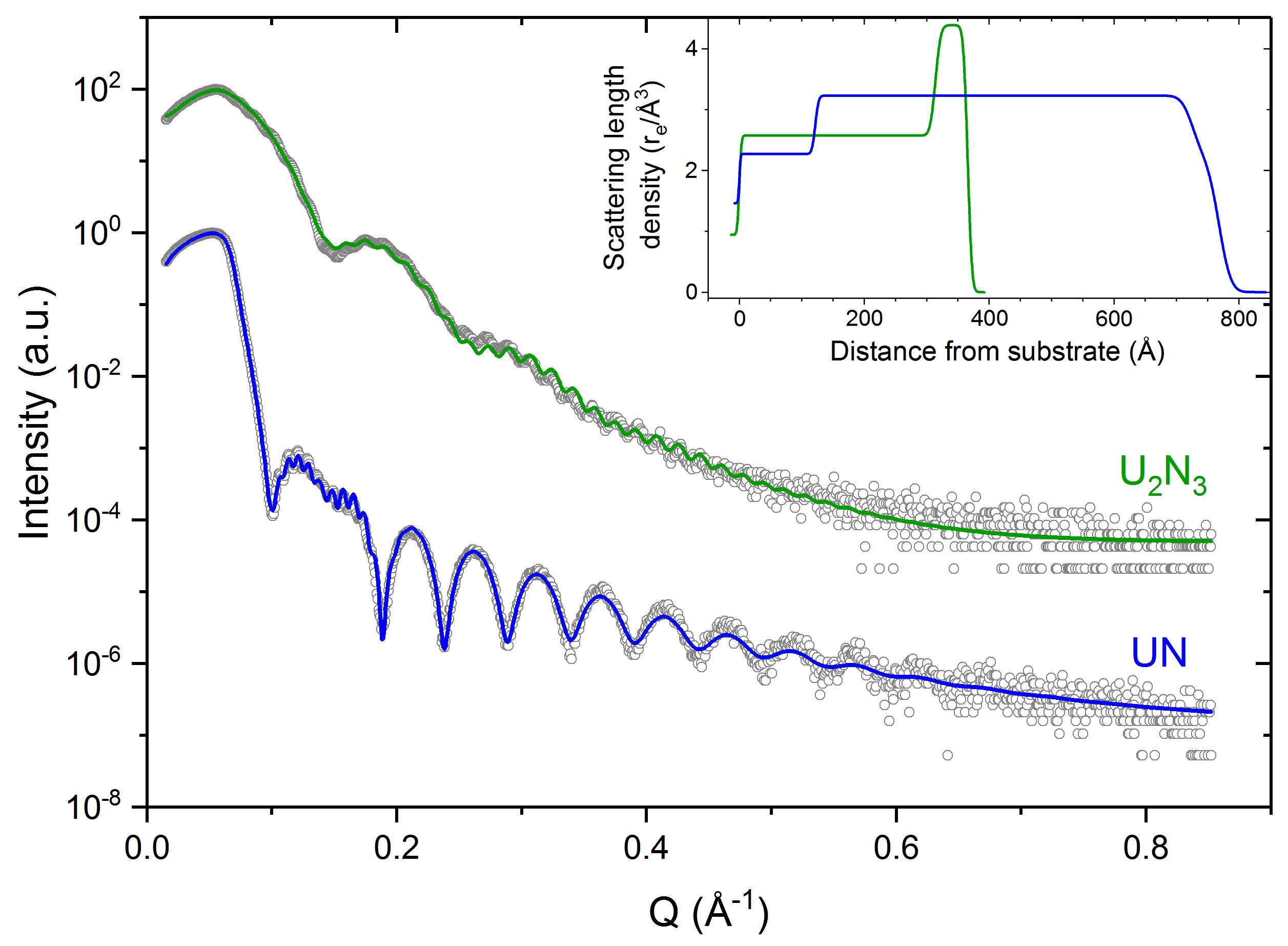
| Sample | Material | Layer | Thickness (Å) | Roughness (Å) | Orientation | (∘) |
|---|---|---|---|---|---|---|
| U2N3 | CaF2 | substrate | - | 2.7 | \hkl[001] | 0.12 |
| U2N3 | film | 310 | 6.8 | \hkl[001] | 0.03 | |
| Au | cap | 50 | 5.4 | polycrystalline | - | |
| UN | Al2O3 | substrate | - | 1.6 | \hkl[1-102] | 0.04 |
| Nb | buffer | 120 | 4.3 | \hkl[001] | 1.22 | |
| UN | film | 600 | 14.2 | \hkl[001] | 1.73 | |
| Nb | cap | 40 | 15.0 | polycrystalline | - |
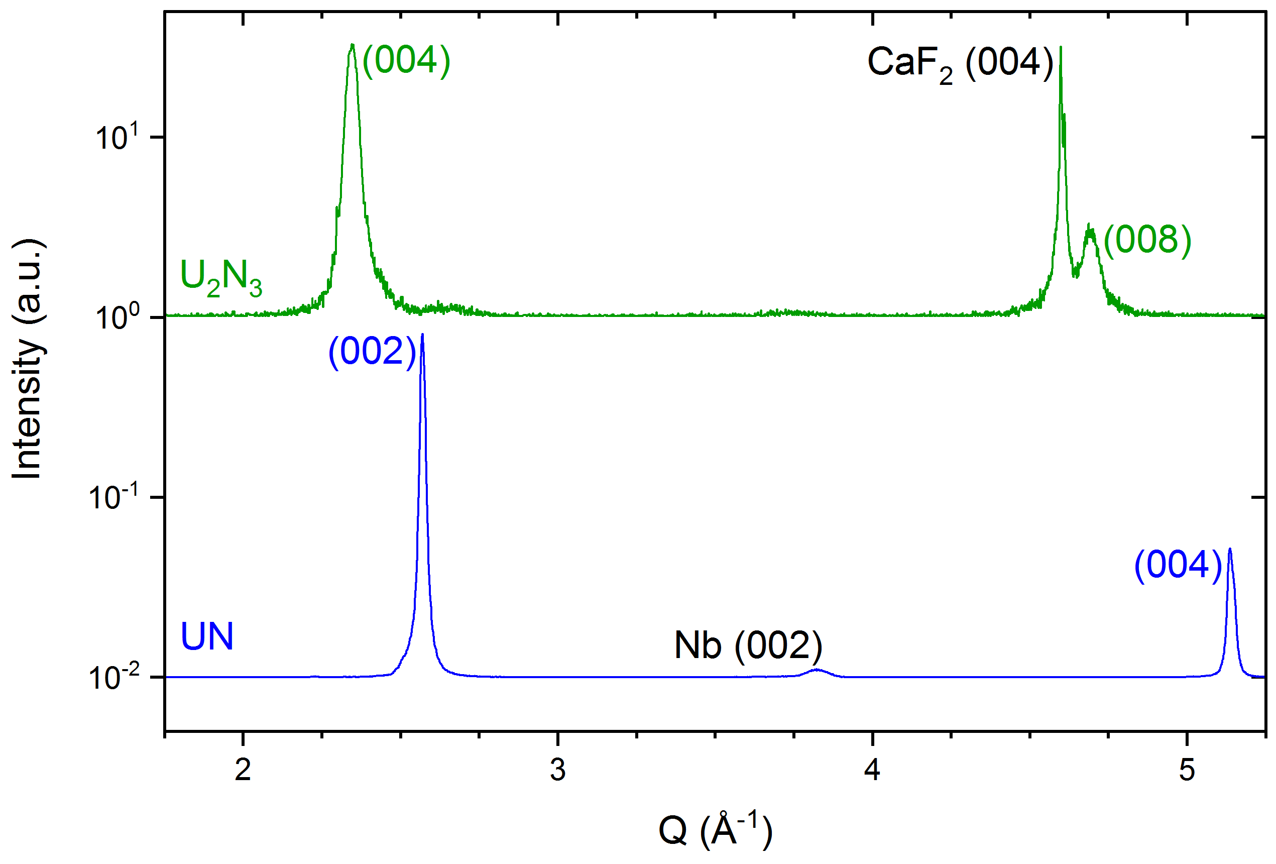
Figure 2 shows the specular 2- XRD scans of the \hkl[001] U2N3 and UN samples, aligned to the specular film peaks. It can be seen that in U2N3 film, grown on CaF2, only the \hkl(004) and \hkl(008) reflections of U2N3 and \hkl(004) reflection of CaF2 are visible, showing the film is highly oriented in this direction. The same is true of the UN film grown on a Nb buffer on Al2O3, with only the \hkl(002) and \hkl(004) reflections of UN and \hkl(002) reflection of Nb visible. From these reflections, it was calculated that the U2N3 lattice parameter (in the specular direction) is 10.720.01 Å and the UN lattice parameter is 4.8950.001 Å.
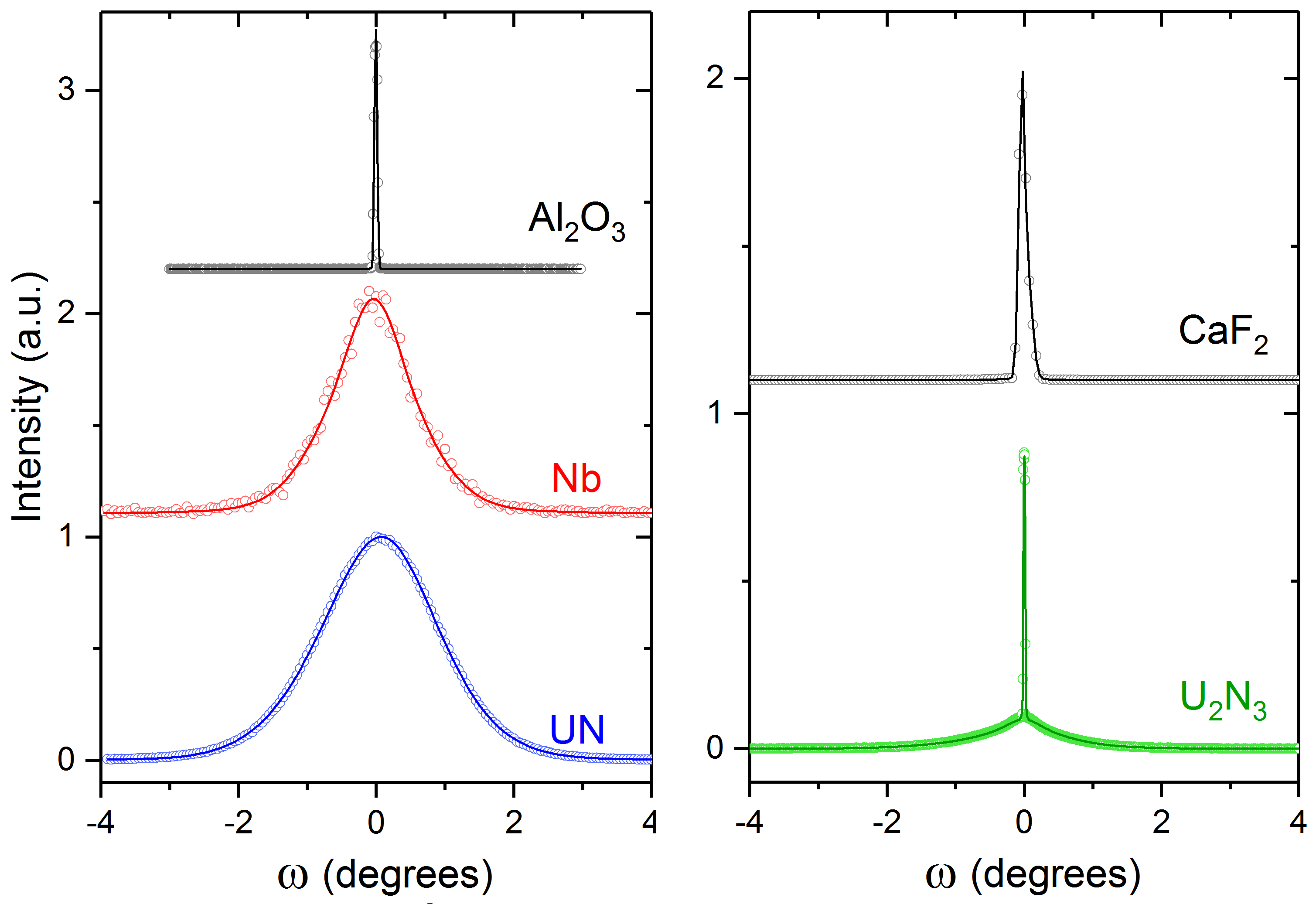
The rocking curves or scans of specular reflections in both the U2N3 and UN samples are shown in Figure 3, and the FWHM () of the fits shown in Table 1. The rocking curve of the \hkl(004) U2N3 reflection is very sharp, with a FWHM of only 0.03 ∘, even narrower than the FWHM of the CaF2 \hkl(004) substrate curve of 0.12 ∘. A low intensity broad component is also present in the is curve, but not seen in that of the CaF2 substrate, showing that there are areas of the U2N3 layer not completely commensurate with the substrate.
In the UN sample, both the Nb buffer and UN layer have broad rocking curves of 1.22 ∘ and 1.73 ∘ respectively, while the substrate curve is much narrower. These large values show that the film layers are not in complete registry with the layer below.
While the specular XRD scans shows only the orientation of this film perpendicular to the surface plane, the in-plane orientation of the \hkl[001] U2N3 and \hkl[001] UN samples can be seen in the scans shown in Figures 4 and 6 respectively.
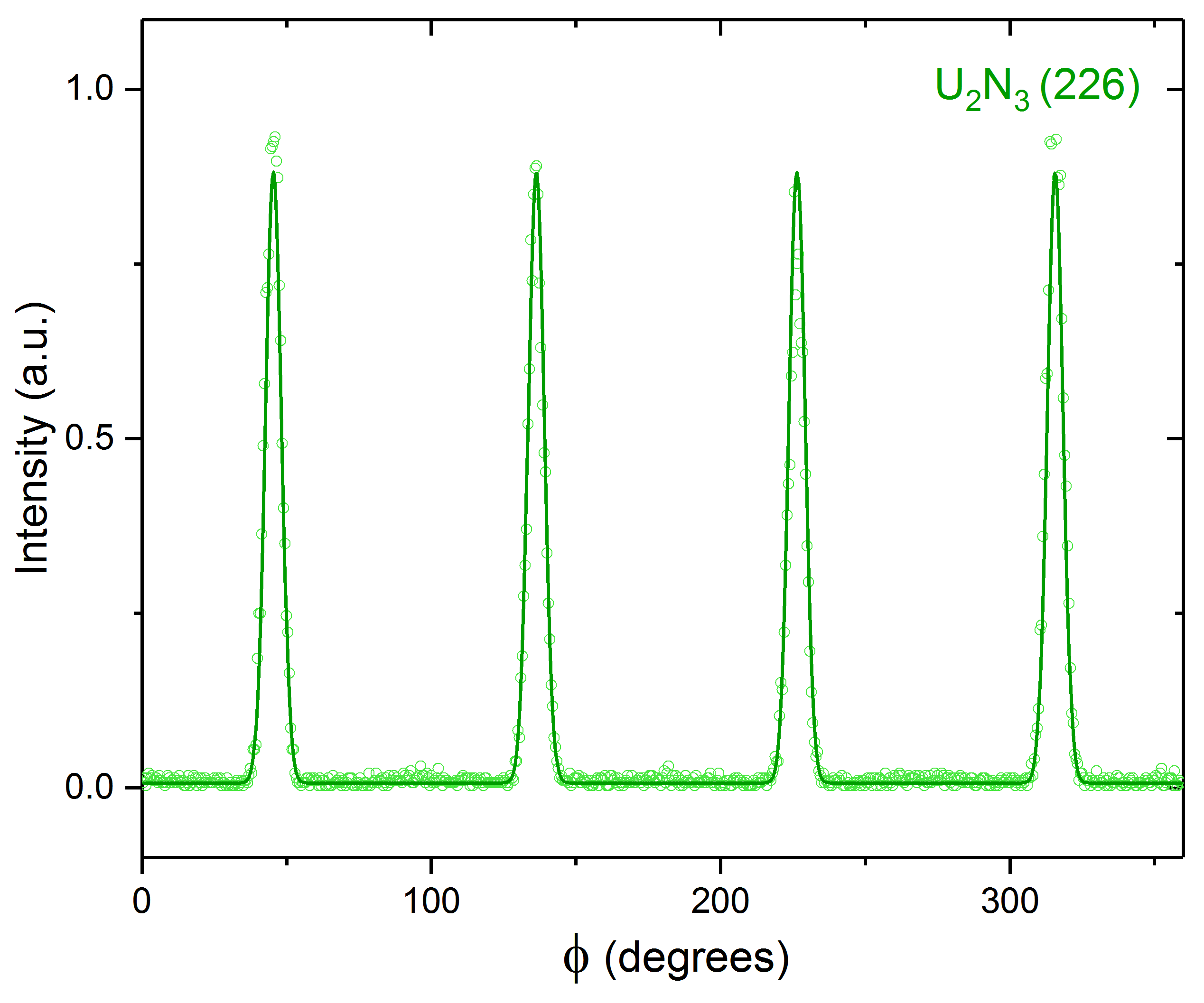
The clear dependence of the off-specular U2N3 \hkl(226) reflection shown in Figure 4 indicates that there is a single domain present in the film. Though not displayed, the off-specular CaF2 reflections showed that the U2N3 film is oriented in the same direction as the substrate. This is depicted in the model of the \hkl(001) planes of each of these in Figure 5, which clearly demonstrates the 2:1 match between the two.
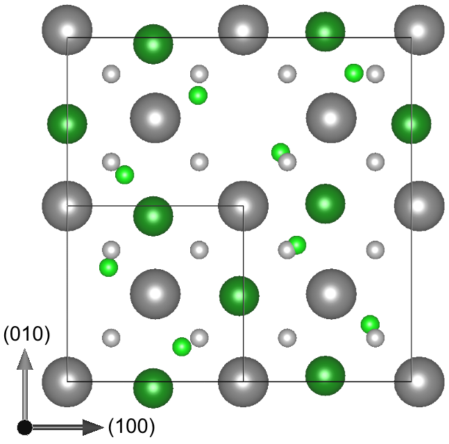
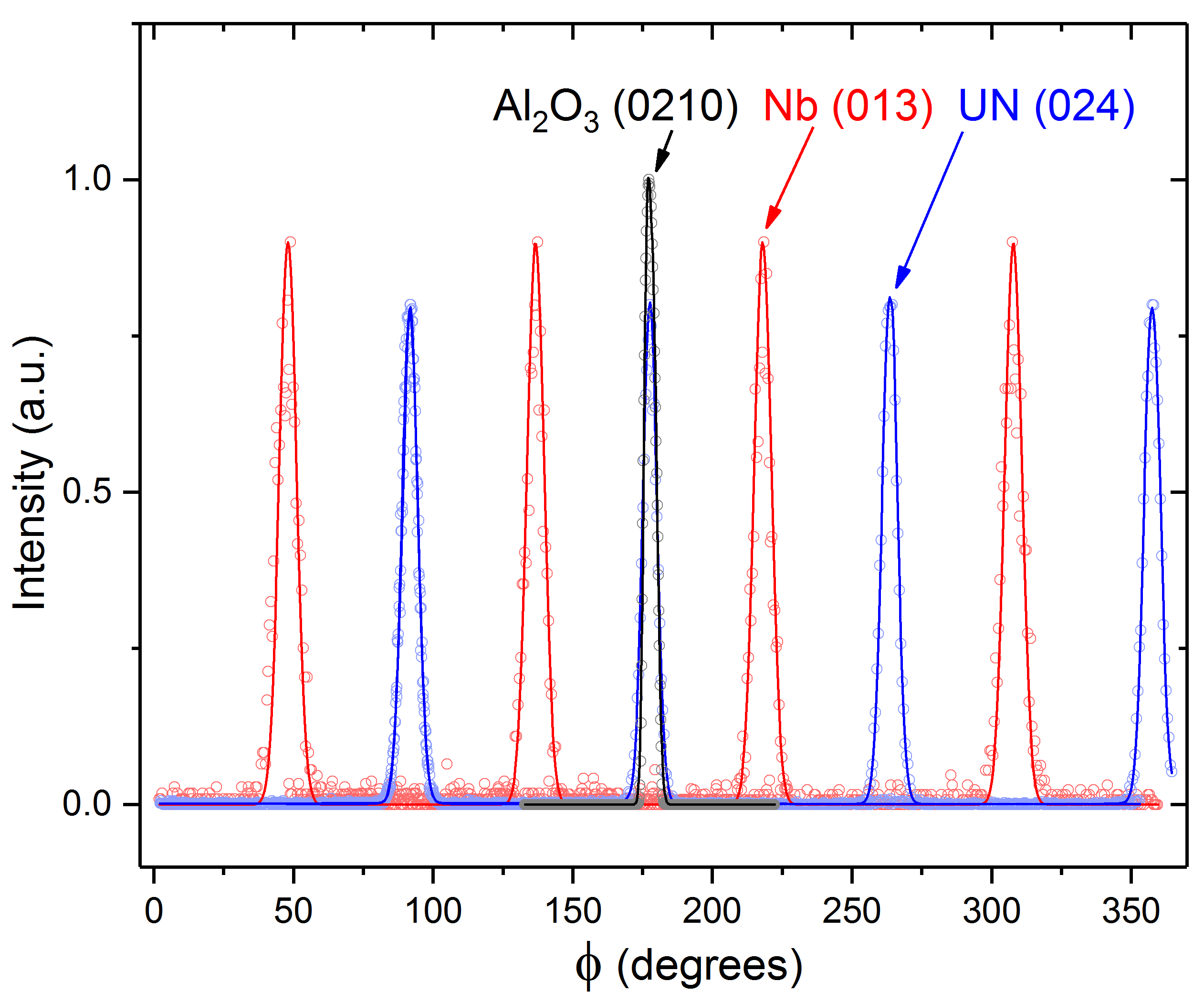
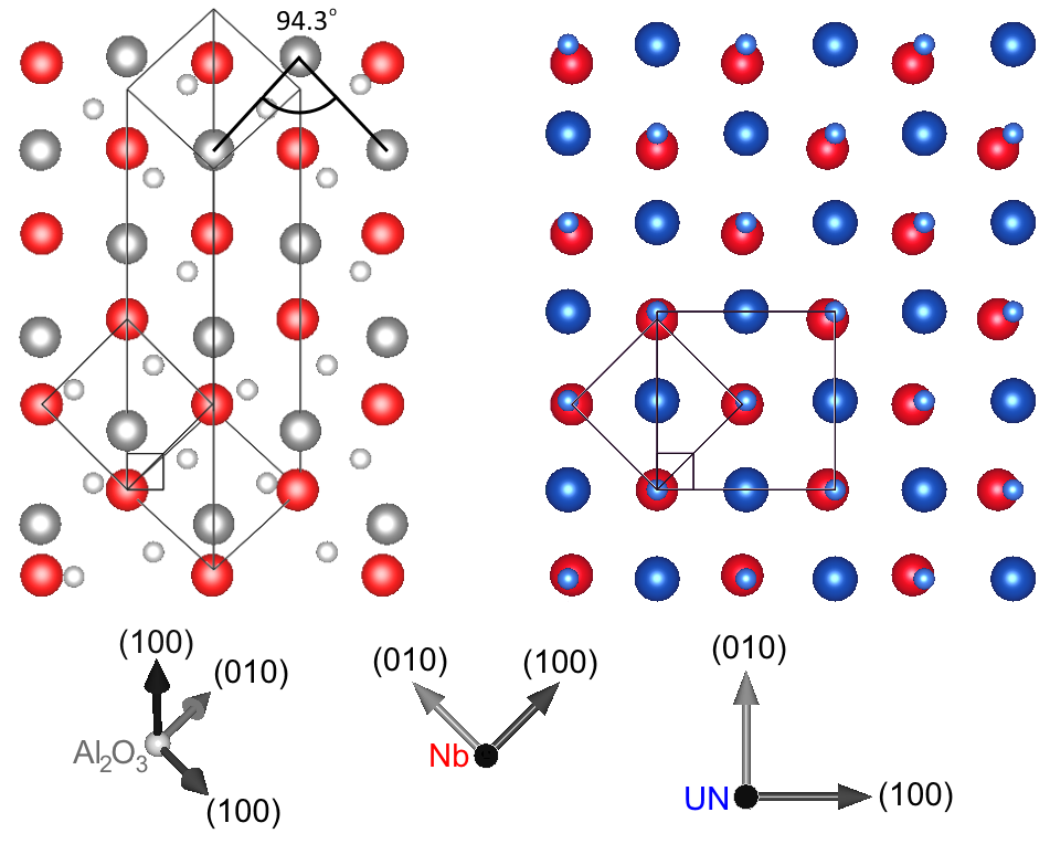
Figure 6 shows that the \hkl(013) Nb and \hkl(024) UN Bragg peaks are dependent on the rotation of the sample, indicating that all crystallites in the \hkl[001] UN sample are of the same orientation. Additionally this figure shows the orientational relationship between the Al2O3 substrate, \hkl[001] Nb buffer, and \hkl[001] UN film. The 45 ∘ difference between the \hkl(013) Nb and \hkl(024) UN peaks indicates the relationship between the buffer and film, as illustrated in the model in Figure 7.
This model shows the close match between the lattices of UN and Nb with a relationship. There also appears to be a close match between the Al2O3 lattice and Nb, however, the Al2O3 lattice in the \hkl[1-102] direction is not square, but rhomohedral, as can be seen by the 94.3 ∘ angle between 3 Al atoms shown in Figure 7. As a rhombus can be considered a tilted square, it is likely this misfit is accommodated for by a tilt of the Nb crystal relative to the Al2O3 substrate such that the \hkl[001] Nb and \hkl[1-102] Al2O3 directions are not parallel. This suggests there is a miscut between the Nb buffer and Al2O3 film, and as the UN film is matched to the Nb buffer, a miscut between the UN film and Al2O3 substrate.
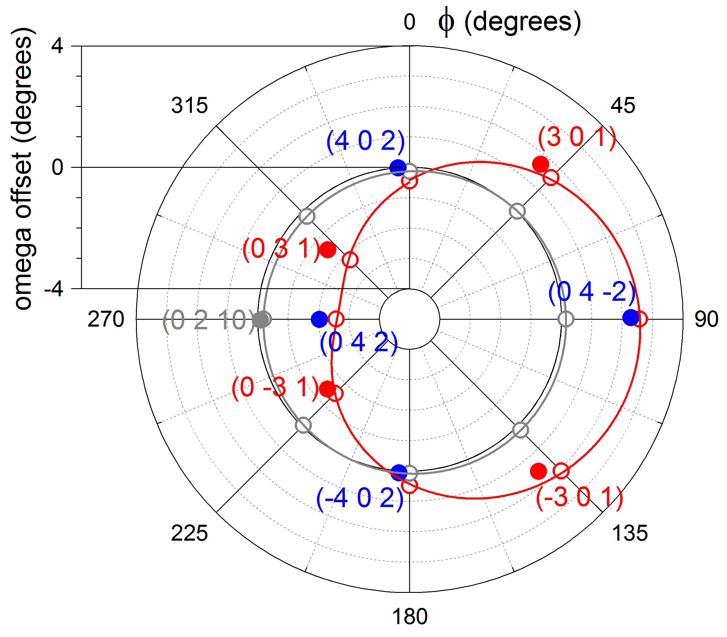
In order to measure this miscut, the omega offset (angle relative to the specular direction) of various Bragg peaks was measured as a function of , sample rotation; the results can be seen in Figure 8. This figure shows labeled off-specular peaks of Al2O3, Nb, and UN as closed gray, red, and blue points respectively. Open points show the specular \hkl(1-102) Al2O3 and \hkl(002) Nb Bragg peaks, fitted to sine functions. The amplitude of this sine function is only 0.2 ∘ for the Al2O3 substrate, showing only a very small miscut between the \hkl[1-102] direction and the surface normal of the sample. However, the amplitude of the sine fit to the Nb specular peaks is 2.6 ∘, with the Nb and UN off-specular peaks also lying close to this fit, showing that there is a large miscut in the \hkl[001] Nb and \hkl[001] UN layers.
III.2 Chemical Characterisation
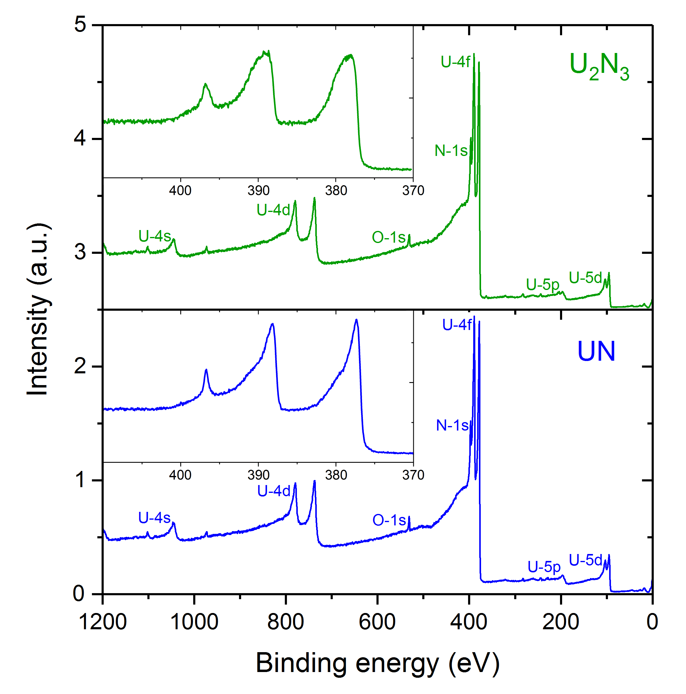
Survey XPS scans taken after Ar sputtering of the \hkl[001] U2N3 and \hkl[001] UN samples, displayed in Figure 9, contain only peaks from U, N, and O contamination. The lack of any peaks from the Nb and Au protective caps as well as Nb buffer and Ca and F substrate show that the spectra is being collected from the U2N3 and UN films only. There are no visible C-1s peaks, showing the lack of carbon contamination in the films. However, the O-1s peak at 531 eV is visible in both the U2N3 and UN films, showing oxygen contamination is present in both samples.
Spectra of the U-4f and N-1s states are inset in Figure 9, and show a clear asymmetry in the U-4f states. This is more pronounced in the UN sample compared to the U2N3, and both the U-4f and N-1s peaks appear narrower in UN.
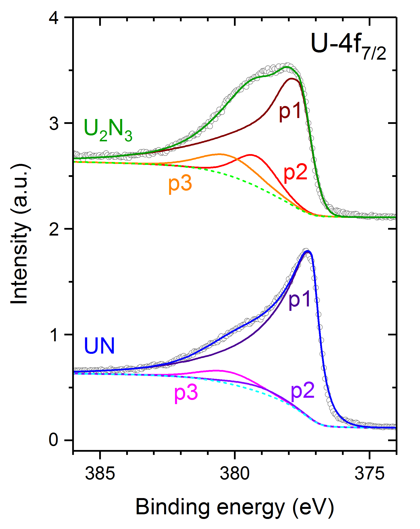
Fitting of the U-4f7/2 peaks, plotted in Figure 10, was performed using a Shirley background and Gaussian-Lorentzian product peaks, where % GL is the percentage of Lorentzian weighting. The lowest binding energy fitted peaks also contained an asymmetric exponential tail modifier, T, with this value and all others peak fit parameters displayed in Table 2.
The fits showed the U-4f7/2 state to be composed of two symmetric peaks at 379.2 eV (p2) and 380.2-380.3 eV (p3) and an asymmetric peak (p1) at lower binding energy for both U2N3 and UN. For UN, this peak was fitted with a narrow FWHM of 0.8 eV, higher asymmetry (low T), and 0.5 eV lower binding energy compared to U2N3. While the area and FWHM of p3 is similar in both UN and U2N3, p2 has a much more significant contribution to the U-4f7/2 state in U2N3 than in UN. The p3 peak, attributed to U(IV), along with the presence of an O-1s peak in the survey scan, show the presence of uranium oxide in the sample Allen et al. (1982).
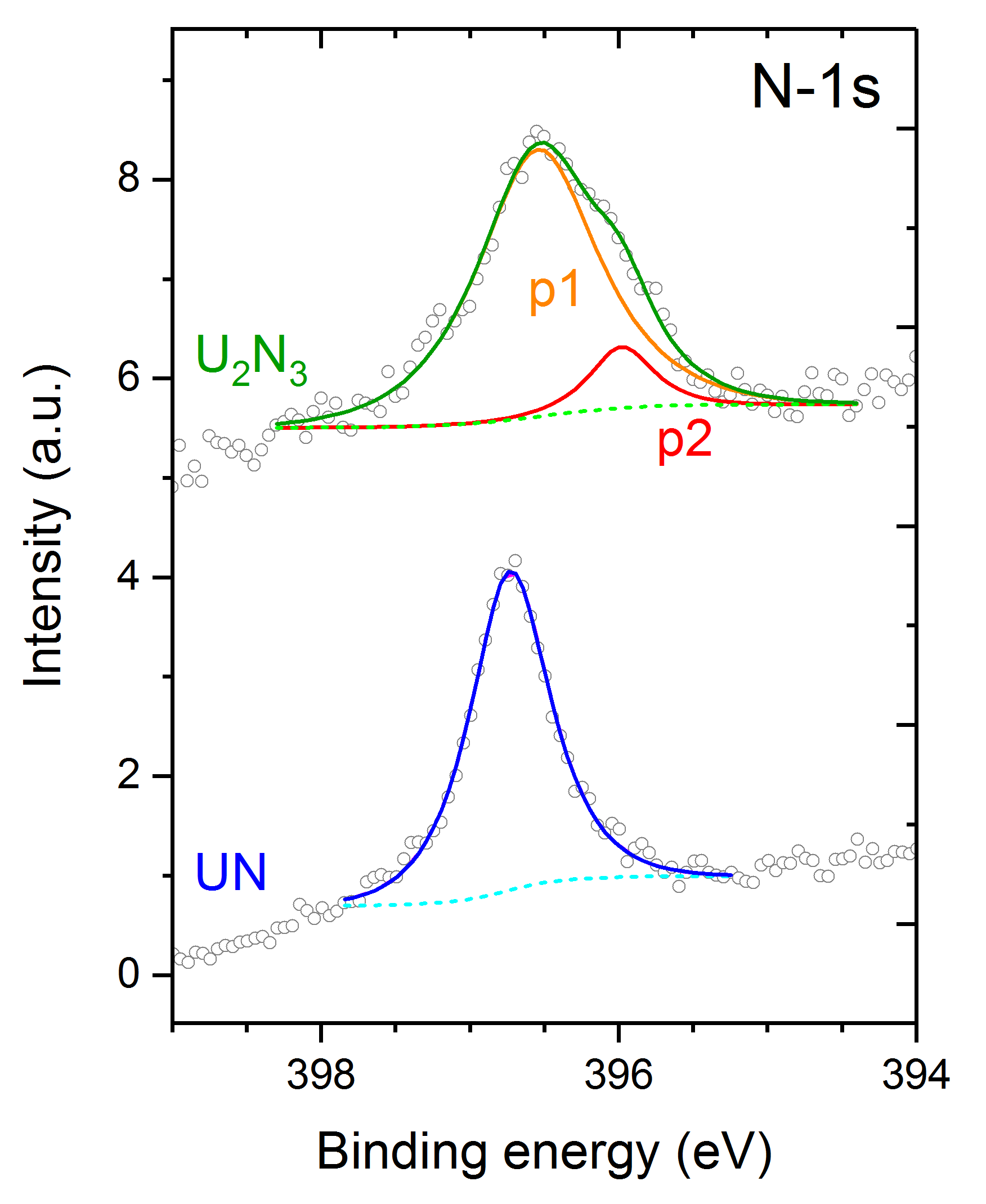
As with the U-4f7/2 state, the N-1s states in U2N3 and UN were fitted with Shirley backgrounds and symmetric Gaussian-Lortenzian peaks, as shown in Figure 11. Fitting of the N-1s state in U2N3 showed it to be composed of peaks at 396.6 eV (p1) and 396.0 eV (p2), with the former having a more significant contribution. In the spectra from the UN sample, the N-1s state was fitted with only a single peak at 0.1 eV higher energy than the main peak in U2N3.
The areas of the fitted peaks are shown in Table 2, with the values normalised to the total area of the U-4f7/2 peak for each sample. Calculations of area ratios between the N-1s and U-4f (p1 and p2 only) were performed using cross sections given by Yeh , and gave values of 1.020.02 and 1.520.04 for UN and U2N3, respectively Yeh and Lindau (1985). The area of p3 in the U-4f7/2 peaks was not included in the calculation as it is attributed to oxide in the sample.
| Sample | Peak | Position (eV) | FWHM (eV) | %GL | T | Area | |
|---|---|---|---|---|---|---|---|
| U2N3 | U-4f7/2 | p1 | 377.7 | 1.1 | 15 | 0.50 | 0.77 |
| U-4f7/2 | p2 | 379.2 | 1.8 | 30 | 0 | 0.12 | |
| U-4f7/2 | p3 | 380.3 | 2.5 | 30 | 0 | 0.11 | |
| N-1s | p1 | 396.6 | 0.9 | 80 | 0 | 0.07 | |
| N-1s | p2 | 396.0 | 0.6 | 80 | 0 | 0.01 | |
| UN | U-4f7/2 | p1 | 377.2 | 0.8 | 90 | 0.38 | 0.90 |
| U-4f7/2 | p2 | 379.2 | 2.3 | 30 | 0 | 0.03 | |
| U-4f7/2 | p3 | 380.2 | 2.5 | 30 | 0 | 0.07 | |
| N-1s | p1 | 396.7 | 0.6 | 80 | 0 | 0.06 |
IV Discussion
The above results clearly show that epitaxial \hkl[001] UN and U2N3 single crystal thin films have been successfully grown for the first time. XRD omega scans performed on the \hkl[001] U2N3 sample demonstrate that the film is in excellent registry with the CaF2 substrate. The lattice parameter of 10.720.01 Å, calculated from 2- scans, is higher than the bulk value of stoichiometric U2N3 of 10.68 Å Rundle et al. (1948). This difference could be caused by strain from the substrate and deviations from stoichiometry.
If this increase in the lattice parameter was caused by strain, a decrease in the and lattice parameter could be expected. Unfortunately, the resolution limits of the x-ray diffractometer used and low number of accessible off-specular peaks do not allow for precise measurements of the in-plane lattice parameters and therefore strain in the film.
U2N3 is know to have a wide range of possible stoichiometries, with ranging from -0.2 to 0.5 in U2N3+x Tagawa and Masaki (1974). While the literature on U2N3+x is sparse, it is known that the lattice parameter of the cubic structure decreases with increasing value of Rundle et al. (1948). As the U2N3 film was deposited at the lowest pressure of N2 found to deposit only single phase U2N3+x, and the lattice parameter is greater than that of stoichiometric U2N3, it is likely that is low. However, XPS area analysis suggests the sample is stoichiometric, within errors.
XPS of the U-4f valence states in the \hkl[001] U2N3 sample yielded results similar to those seen by Long , Wang , and Black Long et al. (2016); Wang et al. (2016); Black et al. (2001). The U-4f7/2 is peak found to be at 377.7 eV, 0.5 eV higher than in UN, and is fitted with an asymmetric peak at this energy, p1, and a symmetric peak at 379.2 eV, p2, which is consistent with the analysis of Wang . While the p1 peak is asymmetric, it is less so than that of UN and U metal, which along with the higher binding energy, show the partial localisation of the 5f states, as described by Black The p2 peak could be attributed to U (III), as seen in U (III) oxyhalidesThibaut et al. (1982). The presence of oxygen contamination in the sample is shown by the small U (IV) peak at 380.2 eV, p3, and the O-1s peak seen in the survey.
While Wang and Long both claim that there is no difference in the N-1s state between UN and U2N3, the present data shows clear evidence of a shoulder at lower binding energy, as well as a 0.1 eV shift in energy of the main component of the peak. It is difficult to determine whether this is present in other literature, as most have lower resolution, and none fit the N-1s peak. There is, however, literature on this second component in other metal nitride systems, such as TiN, where it appears under oxidation and is attributed to the formation of oxynitrides Glaser et al. (2007). However, since the U (IV) peak (p3) in the U2N3 and UN samples are very similar, but this second N-1s component is not present in UN, it is likely that it is not due to oxidation but is instead an indication of the mixed states present in U2N3. The broader FWHM of the main component in the U2N3 N-1s peak of 0.9 eV compared to the 0.6 eV FWHM seen in UN are further evidence of the mixed states in U2N3.
XRD of the \hkl[001] UN sample showed it to be of a single domain, with a lattice parameter of 4.8950.001 Å, close to bulk values, but of much lower quality than the \hkl[001] U2N3 sample. This is evident in the broad rocking curves of both the UN film and Nb buffer layers, as well as the large miscut, which shows a lack of coherence between the Nb buffer and Al2O3 substrate. As the UN film can only be as good quality as the Nb buffer, and Nb growth on \hkl[1-102] Al2O3 growth is shown to be optimised at 800 ∘C, it is unlikely that the quality of the UN film can be improved using this system Claassen et al. (1987). The miscut lying in same plane as the Al2O3 axis and specular direction is consistent with literature, which also shows the \hkl[111] Nb direction to align with the Al2O3 axis Gutekunst et al. (1997). While these papers also find the large miscut between Al2O3 and Nb, none provide the explanation of it arising from the accommodation of the rhombohedral Al lattice in the \hkl(1-102) plane.
Spectra of the U-4f states collected from the UN sample shows sharp asymmetric peaks at higher binding energy than U metal but lower than U2N3, which is comparable to the spectra of Norton , Long , Black , and Wang Long et al. (2016); Wang et al. (2016); Black et al. (2001); Norton et al. (1980). This is indicative of the itinerant nature of the system, as described by Fujimori Fujimori et al. (2012). Slight differences in the spectra arise due to varying levels of oxide in each sample, seen by the U (IV) peak at 380.2 eV. Comparing to the only fitted spectra in the literature and the only spectra taken from a single crystal UN sample, that of Samsel-Czekała , this work shows a much smaller contribution from the peaks at 379.2 eV and 380.2 eV, likely due to the higher purity of the present sample Samsel-Czekała et al. (2007).
V Conclusion
Single crystal UN \hkl[001] and U2N3 \hkl[001] thin films have been successfully deposited via reactive DC magnetron sputtering. XRD analysis shows that both the UN and U2N3 samples are single domain, with specular lattice parameters comparable to bulk values. The U2N3 sample was shown to be of high quality, with good registry to the CaF2 substrate, having a particularly narrow rocking curve. The rocking curve of the UN sample was found to be significantly broader than its Al2O3 substrate, likely due to the large miscut between the substrate and buffer, however, off-specular measurements clearly demonstrate a single domain. Chemical characterisation, conducted via XPS, show the presence oxygen contamination in the thin films. The U-4f peaks were found to be highly asymmetric in the UN sample, indicative of its metallic nature. This was observed to a lesser extent in the U2N3 film. Additionally, the N-1s peak was found to differ between the UN and U2N3 samples, with the latter showing two broader components at lower binding energies.
VI Acknowledgments
The authors are grateful to G. H. Lander for helpful discussions. The authors acknowledge access to the Bristol NanoESCA Facility under EPSRC Strategic Equipment Grant EP/M000605/1 and funding from EPSRC grant 1652612.
VII References
References
- Kurosaki et al. (2000) K. Kurosaki, K. Yano, K. Yamada, M. Uno, and S. Yamanaka, J. Alloys Compd. 311, 305 (2000).
- Terrani et al. (2014) K. A. Terrani, D. Wang, L. J. Ott, and R. Montgomery, J. Nucl. Mater. 448, 512 (2014).
- Dell et al. (1967) R. M. Dell, V. J. Wheeler, and N. J. Bridger, Trans. Faraday Soc. 63, 1286 (1967).
- Sugihara and Imoto (1969) S. Sugihara and S. Imoto, J. Nucl. Sci. Technol. 6, 237 (1969).
- Jolkkonen et al. (2017) M. Jolkkonen, P. Malkki, K. Johnson, and J. Wallenius, J. Nucl. Sci. Technol. 54, 513 (2017).
- Paljević and Despotović (1975) M. Paljević and Z. Despotović, J. Nucl. Mater. 57, 253 (1975).
- Rao et al. (1991) G. A. R. Rao, S. K. Mukerjee, V. N. Vaidya, V. Venugopal, and D. D. Sood, J. Nucl. Mater. 185, 231 (1991).
- Long et al. (2016) Z. Long, L. Luo, Y. Lu, Y. Hu, K. Liu, and X. Lai, J. Alloys Compd. 664, 745 (2016).
- Wang et al. (2016) X. Wang, Z. Long, R. Bin, R. Yang, Q. Pan, F. Li, L. Luo, Y. Hu, and K. Liu, Inorg. Chem. 55, 10835 (2016).
- Lu et al. (2016) L. Lu, F. Li, Y. Hu, H. Xiao, B. Bai, Y. Zhang, L. Luo, J. Liu, and K. Liu, J. Nucl. Mater. 480, 189 (2016).
- Black et al. (2001) L. Black, F. Miserque, T. Gouder, L. Havela, J. Rebizant, and F. Wastin, J. Alloys Compd. 315, 36 (2001).
- Scott et al. (2014) B. L. Scott, J. J. Joyce, T. D. Durakiewicz, R. L. Martin, T. M. Mccleskey, E. Bauer, H. Luo, and Q. Jia, Coord. Chem. Rev. 266, 137 (2014).
- Curry (1965) N. A. Curry, Proceeding Phys. Soc. 86, 1193 (1965).
- Swanson et al. (1953) H. E. Swanson, M. C. Morris, and E. H. Evans, Natl. Bur. Stand. (1953).
- Rundle et al. (1948) R. E. Rundle, N. C. Baenziger, A. S. Wilson, and R. A. McDonald, J. Am. Chem. Soc. 70, 99 (1948).
- Williams and Sambell (1959) J. Williams and R. A. J. Sambell, J. Less Common Met. 1, 217 (1959).
- Barns (1968) R. L. Barns, J. Appl. Phys. 39, 4044 (1968).
- Björck and Andersson (2007) M. Björck and G. Andersson, J. Appl. Crystallogr. 40, 1174 (2007).
- Walton et al. (2010) J. Walton, P. Wincott, N. Fairley, and A. Carrick, Peak Fitting with CasaXPS: A Casa Pocket Book (Accolyte Science, Knutsford, UK, 2010).
- Momma and Izumi (2011) K. Momma and F. Izumi, J. Appl. Crystallogr. 44, 1272 (2011).
- Allen et al. (1982) G. C. Allen, P. M. Tucker, and J. W. Tyler, J. Phys. Chem. 86, 224 (1982).
- Yeh and Lindau (1985) J. J. Yeh and I. Lindau, At. Data Nucl. Data Tables 32, 1 (1985).
- Tagawa and Masaki (1974) H. Tagawa and N. Masaki, J. Inorg. Nucl. Chem. 36, 1099 (1974).
- Thibaut et al. (1982) E. Thibaut, J.-P. Boutique, J. J. Verbist, J.-C. Levet, and H. Noelt, J. Am. Chem. Soc. 104, 5266 (1982).
- Glaser et al. (2007) A. Glaser, S. Surnev, F. Netzer, N. Fateh, G. Fontalvo, and C. Mitterer, Surf. Sci. 601, 1153 (2007).
- Claassen et al. (1987) J. H. Claassen, S. A. Wolf, S. B. Qadri, and L. D. Jones, J. Cryst. Growth 81, 557 (1987).
- Gutekunst et al. (1997) G. Gutekunst, J. Mayer, V. Vitek, and M. Rühle, Philos. Mag. A 75, 1357 (1997).
- Norton et al. (1980) P. R. Norton, R. L. Tapping, D. K. Creber, and W. J. L. Buyers, Phys. Rev. B 21, 2572 (1980).
- Fujimori et al. (2012) S.-i. Fujimori, T. Ohkochi, T. Okane, Y. Saitoh, A. Fujimori, and H. Yamagami, Phys. Rev. B 86, 235108 (2012).
- Samsel-Czekała et al. (2007) M. Samsel-Czekała, E. Talik, P. D. Du Plessis, R. Troc, H. Misiorek, and C. Sulkowski, Phys. Rev. B 76, 144426 (2007).