Two-dimensional topological superconductivity with antiferromagnetic insulators
Abstract
Two-dimensional topological superconductivity has attracted great interest due to the emergence of Majorana modes bound to vortices and propagating along edges. However, due to its rare appearance in natural compounds, experimental realizations rely on a delicate artificial engineering involving materials with helical states, magnetic fields and conventional superconductors. Here we introduce an alternative path using a class of three-dimensional antiferromagnet to engineer a two-dimensional topological superconductor. Our proposal exploits the appearance of solitonic states at the interface between a topologically trivial antiferromagnet and a conventional superconductor, which realize a topological superconducting phase when their spectrum is gapped by intrinsic spin-orbit coupling. We show that these interfacial states do not require fine-tuning, but are protected by asymptotic boundary conditions.
Topological matter represents one of the most intriguing frameworks to realize unconventional physics, due to -dimensional excitations originating from topological properties of the -dimensional systems.Hasan and Kane (2010); Essin and Gurarie (2011); Laughlin (1981) This allows to realize electronic spectra in solid state platforms which resemble those found for some elementary particles in high energy physics and exhibit often an even larger variety. Topologically non-trivial band structures give rise to chiral modes in Chern insulators,Liu et al. (2016) helical modes in quantum spin Hall insulatorsKane and Mele (2005) and Majorana modes in topological superconductors.Leijnse and Flensberg (2012); Kitaev (2001); Fu and Kane (2008) In particular, Majorana zero-energy modes in one-dimensional (1D) topological superconductors have fostered intense research efforts both in their detectionSan-Jose et al. (2015); Oostinga et al. (2013); Ilan et al. (2014) and manipulation,Tanaka et al. (2009); Li et al. (2016); Romito et al. (2012); Halperin et al. (2012) motivated by their potential for topological quantum computing. Nayak et al. (2008); Alicea et al. (2011) Yet, one of the biggest challenges is that nature lacks materials with 1D topological superconductivity, and thus, the only hope for its experimental realization relies on an artificial engineering in nano-structures Nadj-Perge et al. (2014); Mourik et al. (2012); Deng et al. (2012); Finck et al. (2013); Choy et al. (2011); Nadj-Perge et al. (2013); Lutchyn et al. (2010); Röntynen and Ojanen (2015).
Two-dimensional (2D) topological superconductors share the exciting phenomena of their 1D counterparts, while providing additional flexibility. On the one hand, Majorana bound states can be found in vortex cores, Ivanov (2001); Sun et al. (2016); Biswas (2013) which display properties of interest for topological quantum computing.Das Sarma et al. (2006) On the other hand, propagating excitations at edges may allow the exploration of the physics of supersymmetry associated with interacting Majorana fermions. Li et al. (2017); Rahmani et al. (2015a); Hsieh et al. (2016); Rahmani et al. (2015b) However, natural 2D topological superconductors are rather elusive,Mackenzie and Maeno (2003) rendering artificial engineering of 2D topological superconductors an important milestone, very much like their 1D counterparts. This further motivated extensions of the original mechanisms for 1D topological superconductivity to two dimensions, based on topological insulators,Fu and Kane (2008) Yu-Shiba-Rusinov latticesRöntynen and Ojanen (2015) or 2D electron gases with Rashba spin-orbit coupling.Sau et al. (2010)
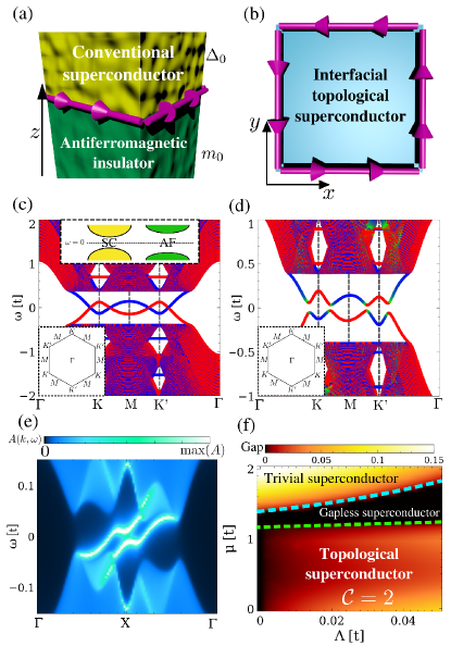
In this letter we introduce an alternative route to create topological superconductivity, exploiting an interface between two bulk ordered phases. Our proposal consists of a heterostructure formed by a insulating bulk antiferromagnet and a conventional bulk superconductor (Fig. 1a). Individually, both systems have an excitation gap, both in the bulk as well as at the surface. However, for a special class of antiferromagnetic insulators, as we will discuss below, protected gapless Andreev bound states emerge at the interface between the two 3D systems. These states are mathematically similar to the Jackiw-Rebbi soliton,Jackiw and Rebbi (1976) so that interfacial zero modes exist independently on how the respective magnitudes and spatial profiles between the two electronic orders are. Furthermore, once intrinsic spin-orbit coupling is introduced, the interface states open a gap, giving rise to a topological superconducting state (Fig. 1b). Therefore, this mechanism shows that antiferromagnetic insulators, commonly overlooked, are potential candidates to engineer topological superconductors.
The key ingredient for our proposal is the existence of Dirac linesKim et al. (2015); Hořava (2005); Schnyder and Ryu (2011); Ryu and Hatsugai (2002); Weng et al. (2015); Hyart et al. (2018); Ezawa (2016); Nandkishore (2016); Shapourian et al. (2018), lines of points in the Brillouin zone where the low energy model is a Dirac equation, in the non-magnetic state of the antiferromagnet. There is no specific requirement for the superconductor, apart from having a conventional s-wave Cooper pairing. For the sake of concreteness, we start by introducing a minimal model that exemplifies such a phenomenology. For this purpose, we take an antiferromagnetic diamond lattice with lattice constant , which can be viewed as a three dimensional analog of the antiferromagnetic honeycomb lattice.Ezawa (2015) Such a structure would be the minimal model for an antiferromagnetic spinel XY2Z4, with the magnetic ions sitting in the X sites. Plumb et al. (2016); Ghara et al. (2017); Ge et al. (2017); Krimmel et al. (2006); Gao et al. (2017) In order to describe the antiferromagnet-superconductor heterostructure, we propose a Hamiltonian consisting of electron hopping , antiferromagnetic ordering , superconducting s-wave pairing , and spin-orbit coupling Fu et al. (2007): with
| (1) |
The parameters are chosen so that the Hamiltonian describes an insulating antiferromagnet for , with magnetization perpendicular to the interface, and a conventional superconductor for . In this way, the electronic spectra of the previous Hamiltonian has an antiferromagnetic gap for and a superconducting gap for . We may take the antiferromagnetic order parameter, the superconducting order parameter, the chemical potential fixing half-filling on the antiferromagnetic side. The parameter controls the smoothness of the change between the two orders, which in the limit becomes sharp. Spin-orbit coupling enters as a next-nearest neighbor hoppingFu et al. (2007) between sites and , and () is the vector between nearest neighbors () and . We denote and the Pauli matrices for the sublattice (A and B) and the spin, respectively. The heterostructure within the lattice is chosen so that the interface (perpendicular to the -axis) consists only of sites belonging to one of the two sublattices, i.e. a zigzag-like interface. Using the standard lattice vectors, we can also define the interface plane by two of them, say and such that the -axis is parallel to .
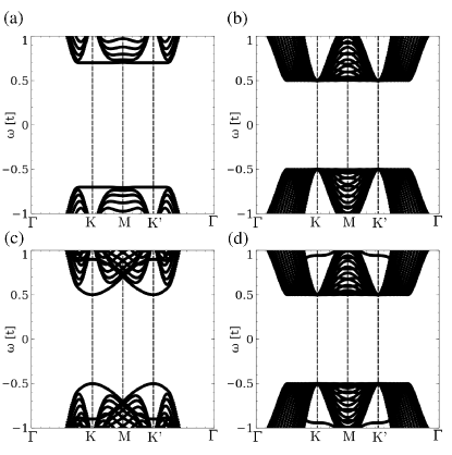
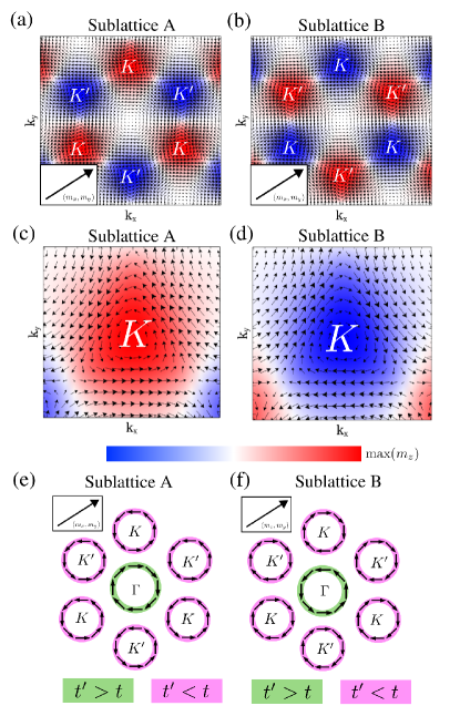
The first interesting finding is that, in the absence of spin-orbit coupling (), the spectrum of the combined structure develops gapless quasiparticle excitations at the interface [Fig. 1(c)]. These gapless Andreev modes are protected against different choices of the interface profile for the antiferromagnetic order, the superconducting order and the chemical potential. Due to their robustness and structure shown below, we refer to these protected Andreev modes as solitonic states. Switching on spin-orbit coupling leads to a fully gapped spectrum for the solitonic states [Fig. 1(d)]. The second remarkable observation is the appearance of the topological Chern invariant for the gapped system, indicating the presence of two propagating Majorana modes at the edges of the interface [Fig. 1(e)]. This chiral state relies on the broken time reversal symmetry due to the antiferromagnetic order.
The emergence of this topological insulating state by combining two topologically trivial insulating systems is the main finding of our manuscript. This topological superconducting state is robust upon changing parameters [Fig. 1(f)], raising two questions. First, why the interface between the two topologically trivial gapped materials shows robust zero energy modes? Second, why including a small spin-orbit coupling gives rise to a topological superconducting state?
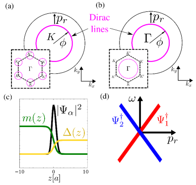
We first address the origin of the gapless interface states, starting with the Bloch Hamiltonian for the pristine diamond lattice , where , with the lattice vectors of the fcc lattice, and corresponds to the cubic symmetry. The spectrum possesses lines in -space where the valence and conduction band touch. The projected two-dimensional Brillouin zone (BZ) perpendicular to the -axis is hexagonal with the point (line) in the center and the and points (lines) at the boundary. Depending on the ratio , one Dirac line forms around the point or two disconnected Dirac lines form around and points [Figs. 2(a,b)]. Hyart et al. (2018) Focusing on such a Dirac line, we can formulate an effective low-energy Hamiltonian We use that the momentum is tied to the reference frame of the line, such that is tangential to the line, perpendicular to the line and the -axis and perpendicular to the two other components, slightly tilted with respect to the -axis. This low-energy model allows us to study the interface between the superconductor and antiferromagnet analytically. Using the spatially dependent order parameters and as introduced above, the effective Hamiltonian takes the form
| (2) |
where is the conserved Bloch momentum parallel to the interface, sum runs over the two sites and .
The Hamiltonian (2) defines a system which is inhomogeneous along the -direction, where for the Hamiltonian is purely antiferromagnetic and for purely superconducting. Remarkably, for and a profile fulfilling these asymptotic conditions, two solitonic zero-energy Andreev modes exist localized at the interface (Fig. 2c), with the following ansatzJackiw and Rebbi (1976); San-Jose et al. (2015)
| (3) |
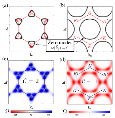
where , as the normalization constant and as branch index. Note that although these states are pinned to zero energy, they are not Majorana modes. Furthermore, such states will also exist in the more generic case and . Away from , the two solitonic wave functions have a finite energy dispersion in the direction of the radial momentum (Fig. 2d), yielding the effective Hamiltonian . The existence of these states for each point of the Dirac line implies that the zero mode surface of the heterostructure reflects the original Dirac lines of the antiferromagnet. Thus, any change of the Dirac line structure would be reflected in these zero-energy interface modes, as shown in Figs. 3ab.
In a next step, we introduce the intrinsic spin-orbit coupling, equivalent to a momentum and sublattice dependent exchange field. In the vicinity of the Dirac lines it takes the effective form , where denotes the position on the Dirac line as shown in Fig. 2(a,b). We note that for the different situations of the Dirac lines the SOC takes a vortex-like profile, but with opposite vorticities around and . By projecting the spin-orbit coupling term onto the solitonic basis, we arrive to the following low-energy Hamiltonian,
| (4) |
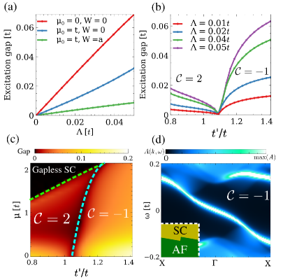
where generates a gap in the spectra and finite Berry curvature where the zero modes were located [Figs.3(cd)]. The gap is linear in the spin-orbit coupling and depends on the chemical potential and the profile width [Fig. 4(a)]. This Hamiltonian has the structure of a chiral p-wave superconductor, since the spin-orbit coupling takes the form of a chiral gap function. In this way, the superconducting phase in the interface acquires chirality with a non-vanishing Chern number, if .
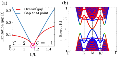
The Lifshitz transition found in the paramagnetic phase of the antiferromagnetic side by varying the hopping ratio [Figs2(a,b)] has a final consequence for the gapped interface modes: this Lifshitz transition introduces a topological transition for the superconducting phase of the heterostructure. For each of the two Dirac lines contributes through a single phase winding adding together to a Chern number [Fig.3(c)], while for there is only a single Dirac line winding in opposite orientation around leading to for the interface superconductor [Fig.3(d)]. Due to corrections to the low energy model, the topological phase transition found by exactly solving the model does not coincide perfectly with the bulk Lifshitz transition, but happens at slightly higher than , as visible in Fig. 4(b), which shows a gap closing at this transition point. This specific transition point depends on the chemical potential as shown in Fig. 4(c), depicting a phase diagram with two topological phase transitions, from a gapless superconductor to the topological sector and then . Our calculations demonstrate that the topological phases are robust, and their existence does not depend on details of the electronic structure of the superconductor, but is determined by the topology of the Dirac lines of the magnetic side. Since the symmetric case belongs to the sector , the sector could be reached through uniaxial strain perpendicular to the interface, increasing .
A last important issue, especially for future experimental realizations, is whether topological phases are sensitive to the quality of the interface. To test this we now consider a saw-shaped interface, i.e. a tilted interface orientation yielding a periodicity of the original unit cell. We observe that even for this ”imperfect” heterostructure the interface develops a topological phase with for [Fig. 4(d)]. The inter-valley scattering induced by the interface supercell shifts the system to the sector . Similar results are obtained for other interface orientation, with the exception of the armchair interface where the two sublattice sites appear in equal number at the interface. This result demonstrates that the topological phase can be ascribed to the robustness of the parent solitonic states and generically requires an imbalance between the two sublattice sites.
Using a minimal model, we have shown how to engineer topological superconductivity connecting an insulating antiferromagnet with a conventional superconductor. While we use a single-orbital model, multi-orbital extensions of Eq. 1 could, for example, capture the physics of antiferromagnetic spinels, such as CoAl2O4, that realizes an insulating antiferromagnetic diamond lattice,Ghara et al. (2017) but it is unclear so far whether this material generates in the paramagnetic state the necessary Dirac lines. Finally, it is important to notice that the phenomenology presented here is not restricted to antiferromagnets on diamond lattices, but will emerge in generic systems displaying this kind of Dirac lines, which would enlarge the range of potential candidate materials.Kim et al. (2015); Hořava (2005); Schnyder and Ryu (2011); Ryu and Hatsugai (2002); Weng et al. (2015); Hyart et al. (2018); Ezawa (2016) Such kind of antiferromagnets would constitute an invaluable building block to engineer two-dimensional topological superconductors without fine tuning requirements, robust against imperfections and changes of materials, providing a new platform to study Majorana physics.
Acknowledgements We would like to thank F. von Oppen, T. Neupert, F. Guinea, A. Ramires and Y. Maeno for helpful discussions. J.L.L is grateful for financial support from ETH Fellowship program. M.S. acknowledges the financial support by the Swiss National Science Foundation through Division II (No. 163186). We acknowledge financial support from the JSPS Core-to-Core program ”Oxide Superspin” international network.
APPENDIX
Appendix A Structure of the diamond lattice and the heterostructure
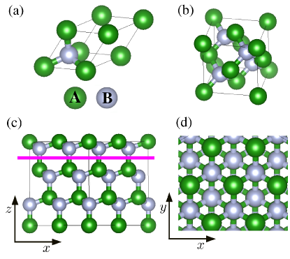
Here we briefly discuss the spatial structure of the tight binding scheme employed to model a Dirac line material. We use a single orbital tight binding model, whose sites are located in a diamond lattice. This model can be understood as a three-dimensional extension of a honeycomb lattice. The unit cell has two sites, labeled A and B (Fig. 5a). The bulk structure can be understood as two interpenetrating fcc lattices as shown in Fig. 5b.
The heterostructures considered in our manuscript are obtained by growing the diamond lattice along the (1,1,1) direction of the lattice shown in Fig. 5b. A sketch of such heterostructure in shown in Fig. 5c, where the purple line mark the interface plane between the antiferromagnetic and superconducting parts. The heterostructure can be understood as stacked buckled honeycomb lattices. Finally, Fig. 5d shows a top view of the interface, showing a triangular lattice whose Brillouin zone will be hexagonal.
Appendix B Spectra of isolated AF and SC
We first briefly discuss the electronic spectra for isolated bulk superconducting and antiferromagnetic states separately. In the absence of spin-orbit coupling, both electronic spectra show a gap, as shown in Fig. 6 (a,b), whose magnitude is controlled by for the antiferromagnet and for the superconductor. Including spin-orbit coupling slightly modifies the spectra but maintains the gap [Fig. 6 (c,d)]. This highlights that spin-orbit coupling does not create a strong change in the electronic structure for the bulk system.
Appendix C Spin texture induced by spin-orbit coupling
We now discuss in more in detail the effect of spin-orbit coupling, that enters in the Hamiltonian as a momentum and sublattice dependent exchange coupling . In Fig. 7 we show the spin-texture induced by the spin-orbit coupling, projected onto the Bloch momentum parallel to the interface . We observe opposite sign for the spin texture on the two sublattices, naturally connected by the combination of time reversal and inversion symmetry operation. The exchange field induces a vortex structure of the spin textures around the and point as well as around the point. This is responsible for the chirality and the structure of the gapped topological interface states. The reciprocal spin texture vanishes in the point as required by time-reversal symmetry, allowing for a gap closing in the context of the Lifshitz and the topological phase transition.
This in-plane spin texture round the , and points can be captured by a reduced effective Hamiltonian of the form The winding is visible through the phase factor of the off-diagonal matrix elements parametrized by the polar angles and for a circle around the corresponding centers. Ignoring corrections due to irrelevant details of the band structure, the spin-orbit coupling term can be written as
| (5) |
in the vicinity of the () point and
| (6) |
around . Note that the main the sign change in the effective exchange field for the two cases, that is visible in the corresponding vorticity in Fig. 7.
Appendix D Interface zero-energy states
We now discuss the analysis of the interface states based on an effective one-dimensional Dirac equation with a spatially dependent antiferromagnetic ordering and onsite s-wave pairing, that would arise for the different contained in the Dirac line. This model allows for a decoupling into two separate sectors, one for spin-up electrons and spin-down holes and another for spin-down electrons and spin-up holes, with operators and , respectively,
| (7) |
where
| (8) |
| (9) |
| (10) |
| (11) |
at . The superconducting and antiferromagnetic ordering are general functions of , so that and . We will impose the asymptotic conditions , , and , with and positive real numbers. Taking , the following two spinors
| (12) |
| (13) |
are eigenvectors fulfilling and as expected for a zero-energy state. It is important to note that such zero-energy solutions exist for any profile and provided the asymptotic conditions are fulfilled, and can be understood as solitonic solutions between a Dirac antiferromagnet and a Dirac superconductor. In terms of field operators, the zero-energy solutions take the simple product form
| (14) |
with and a normalization constant as stated in the main text. We finally note that a zero energy solution generically exists provided and . Therefore, our proposal will also hold in the presence of both superconductivity and antiferromagnetism in the heterostructure, as long as for the antiferromagnetic gap is bigger than the superconducting gap and for the superconducting gap is bigger than the antiferromagnetic gap.
This calculation assumes in the superconducting part. For a generic situation with , our numerical calculations show that the zero energy states still appear, but at slightly shifted from the Dirac lines.
Appendix E Gap opening in interfacial states
Next we consider possible terms in the Hamiltonian that could open a gap in the interfacial edge states. For that, we will consider several one-body perturbations, and we will project them onto the solitonic subspace. We take a basis that accounts for the two interfacial states as they will not be independent anymore,
| (15) |
In this basis, the two interface states are now represented as with
| (16) |
such that the projection operator in the manifold takes the form
| (17) |
Given a certain perturbation of the form in the original basis, its representation in the solitonic basis, , is obtained as . With the previous representation, projecting the different operators simply consists of multiplying the relevant matrix elements. The first perturbation that we will consider is a sublattice independent exchange field, which takes the form
| (18) |
with a generic function. Projecting this in the matrix representation yields immediately zero due to the sublattice structure of . Hence no sublattice independent local exchange can break the degeneracy of the solitonic states, at least to first order. In particular, this implies that an external in-plane magnetic field and a sublattice-independent Rashba spin-orbit coupling will not open up a gap.
The next perturbation that we will consider is a sublattice dependent exchange field, even in momentum,
| (19) |
with . Once more the projection on the solitonic states is zero, but now the reason lies in the relative phases between electron and hole sectors. This perturbation would arise from rotating the axis of the staggered moment of the antiferromagnet. The degeneracy results from the spin rotational symmetry of the energy spectra.
Finally, we consider a sublattice dependent exchange field that is odd in momentum,
| (20) |
with . In this case the projection does not vanish as it fits to the relative phase structure of electrons and holes. Such an odd-momentum exchange term arises from spin-orbit coupling, which includes the sign change between the sublattices due to inversion symmetry. To summarize, a perturbation opening a gap in the solitonic states must fulfill the following conditions
| (21) |
where and and are time reversal and inversion symmetry operators.
Appendix F Calculation of the Chern number
We start with the effective Hamiltonian for the low-energy Andreev modes around the Dirac lines with
| (22) |
where and . By performing a change of variable the Hamiltonian can be rewritten as
| (23) |
with and . This Hamiltonian describes a skyrmion in reciprocal space with the variables and . The Berry curvature associated with the low-energy state of this Hamiltonian corresponds to a magnetic monopole in reciprocal space. Thus, the calculation of the Chern number simply yields the charge of the monopole . This leads to a Chern number for the and point which add up to . For the -point the skyrmion is reversed leading to the Chern number . The topological phase transition connects the phase with and .
Appendix G Spatial dependence of the gap
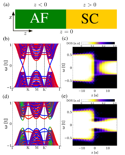
In this section we show how the topological gap evolves as one moves in the heterostructure from superconducting to the antiferromagnetic part in the direction. In the topological state, the gap remains open as one goes away from the interface in the z-direction. In the direction of the antiferromagnet the gap converges to , whereas in the direction of the superconductor it converges to . To rationalize this, it is illustrative to compute the density of states (DOS) the heterostructure as shown in Fig. 8a, where show two different situations: a gapless state which arises for zero spin-orbit coupling (Figs. 8bc), and gapped situation that arises when taking (Figs. 8de). The computation of the density of states can be performed by means of the Green function of the heterostructure as , with the Green function of the heterostructure, the energy, the in-plane Bloch momenta and the vertical coordinate in the heterostructure.
Both in the absence () and presence () of spin-orbit coupling, it is observed that in the antiferromagnetic region , the local gap converges to the antiferromagnetic gap , whereas in the superconducting region it converges to the superconducting gap (Figs. 8ce). In the absence of spin-orbit coupling (Figs. 8bc), the density of states at the interface becomes gapless, signaling the existence of the gapless modes in that region. In comparison, for (Figs. 8de) the density of states remains gapped at the interface. Therefore, in the case of a topological gap (Figs. 8bc), the system remains fully gapped for every point of the heterostructure.
Appendix H Strain driven topological phase transition
Here we briefly discuss details on the gap closing for the topological phase transition with strain between and . The gap closing occurs at the M points, where the spin-orbit coupling vanishes for symmetry reasons. To illustrate this, we show in Fig. 9a the evolution of the gap with uniaxial strain, both in the M point and in the full Brillouin zone. In this way, when the interfacial zero modes are located at the M point, that happens at the critical strain marker with a purple circle in Fig. 9a, the system remains gapless even in the presence of spin-orbit coupling, as shown in Fig. 9b. For strains in which there is a finite gap, the gap is generically not located at the M point but at some arbitrary point in the Brillouin zone, close to the location of the Dirac lines.
Appendix I Possible candidate materials
The main limitation of our model is that we cannot unequivocally assess if a specific complex material would be suitable for our proposal. An analogous analysis to the one presented in our manuscript could be performed by combining density functional theory and Wannierization,Marzari et al. (2012) which allows obtaining a multiorbital Hamiltonian from first principles. Xu et al. (2011); Garrity and Vanderbilt (2013); Feng et al. (2018) In that way, it would be possible to asses from first principles if a certain material would be suitable for the mechanism presented.
As mentioned in the manuscript, a possible candidate for our proposal is CoAl, that is experimentally known to realize an antiferromagnetic diamond lattice, giving rise to a multiorbital version of the tight binding model of our manuscript. Interestingly, spinels compounds have been proposedSteinberg et al. (2014); Wan et al. (2012); Xu et al. (2011) to show Dirac and Weyl like crossings, in particular CaOs2O4 Wan et al. (2012), SrOs2O4 Wan et al. (2012) and HgCr2Se4Xu et al. (2011). Assessing whether if CoAl has Dirac lines in the paramagnetic state requires first principles density functional theory calculations, which is beyond the scope of our study. Nevertheless, given that similar compounds are known to show Dirac-like physics, it is likely that CoAl could realize the required electronic structure for our proposal.
Assuming that CoAl2O4 hosts the necessary gapped Dirac lines, it is still necessary to assess the value of the topological gap, controlled by spin-orbit coupling of the antiferromagnetic and superconductor. In the following we will take as the antiferromagnet CoAl2O4 and as superconductor the spinel compound LiTi2O4Sun et al. (2004); Jin et al. (2015), that has a superconducting gap meV. In a low energy Hamiltonian, the effective spin-orbit coupling can be reduced by an order of magnitude with respect to the atomic value due to its interplay with crystal field effects.Xiao et al. (2011) Taking into account that the atomic spin-orbit coupling in 3d transition metals is on the order of 20 meV,Baumann et al. (2015) we would have meV for the effective low energy Hamiltonian. Therefore, according to the previous discussion for a CoAl2O4/LiTi2O4 heterostructure, we may expect a topological gap on the order of 0.4 meV, which can be observed experimentally and is on the same order of magnitude of state-of-the-art experimentsZhang et al. (2018, 2017).
References
- Hasan and Kane (2010) M. Z. Hasan and C. L. Kane, Rev. Mod. Phys. 82, 3045 (2010).
- Essin and Gurarie (2011) A. M. Essin and V. Gurarie, Phys. Rev. B 84, 125132 (2011).
- Laughlin (1981) R. B. Laughlin, Phys. Rev. B 23, 5632 (1981).
- Liu et al. (2016) C.-X. Liu, S.-C. Zhang, and X.-L. Qi, Annual Review of Condensed Matter Physics 7, 301 (2016).
- Kane and Mele (2005) C. L. Kane and E. J. Mele, Phys. Rev. Lett. 95, 226801 (2005).
- Leijnse and Flensberg (2012) M. Leijnse and K. Flensberg, Semiconductor Science and Technology 27, 124003 (2012).
- Kitaev (2001) A. Y. Kitaev, Physics-Uspekhi 44, 131 (2001).
- Fu and Kane (2008) L. Fu and C. L. Kane, Phys. Rev. Lett. 100, 096407 (2008).
- San-Jose et al. (2015) P. San-Jose, J. L. Lado, R. Aguado, F. Guinea, and J. Fernández-Rossier, Phys. Rev. X 5, 041042 (2015).
- Oostinga et al. (2013) J. B. Oostinga, L. Maier, P. Schüffelgen, D. Knott, C. Ames, C. Brüne, G. Tkachov, H. Buhmann, and L. W. Molenkamp, Phys. Rev. X 3, 021007 (2013).
- Ilan et al. (2014) R. Ilan, J. H. Bardarson, H. Sim, and J. E. Moore, New Journal of Physics 16, 053007 (2014).
- Tanaka et al. (2009) Y. Tanaka, T. Yokoyama, and N. Nagaosa, Phys. Rev. Lett. 103, 107002 (2009).
- Li et al. (2016) J. Li, T. Neupert, B. A. Bernevig, and A. Yazdani, Nature Communications 7, 10395 (2016).
- Romito et al. (2012) A. Romito, J. Alicea, G. Refael, and F. von Oppen, Phys. Rev. B 85, 020502 (2012).
- Halperin et al. (2012) B. I. Halperin, Y. Oreg, A. Stern, G. Refael, J. Alicea, and F. von Oppen, Phys. Rev. B 85, 144501 (2012).
- Nayak et al. (2008) C. Nayak, S. H. Simon, A. Stern, M. Freedman, and S. Das Sarma, Rev. Mod. Phys. 80, 1083 (2008).
- Alicea et al. (2011) J. Alicea, Y. Oreg, G. Refael, F. von Oppen, and M. P. A. Fisher, Nature Physics 7, 412 (2011).
- Nadj-Perge et al. (2014) S. Nadj-Perge, I. K. Drozdov, J. Li, H. Chen, S. Jeon, J. Seo, A. H. MacDonald, B. A. Bernevig, and A. Yazdani, Science 346, 602 (2014).
- Mourik et al. (2012) V. Mourik, K. Zuo, S. M. Frolov, S. R. Plissard, E. P. A. M. Bakkers, and L. P. Kouwenhoven, Science 336, 1003 (2012).
- Deng et al. (2012) M. T. Deng, C. L. Yu, G. Y. Huang, M. Larsson, P. Caroff, and H. Q. Xu, Nano Letters 12, 6414 (2012).
- Finck et al. (2013) A. D. K. Finck, D. J. Van Harlingen, P. K. Mohseni, K. Jung, and X. Li, Phys. Rev. Lett. 110, 126406 (2013).
- Choy et al. (2011) T.-P. Choy, J. M. Edge, A. R. Akhmerov, and C. W. J. Beenakker, Phys. Rev. B 84, 195442 (2011).
- Nadj-Perge et al. (2013) S. Nadj-Perge, I. K. Drozdov, B. A. Bernevig, and A. Yazdani, Phys. Rev. B 88, 020407 (2013).
- Lutchyn et al. (2010) R. M. Lutchyn, J. D. Sau, and S. Das Sarma, Phys. Rev. Lett. 105, 077001 (2010).
- Röntynen and Ojanen (2015) J. Röntynen and T. Ojanen, Phys. Rev. Lett. 114, 236803 (2015).
- Ivanov (2001) D. A. Ivanov, Phys. Rev. Lett. 86, 268 (2001).
- Sun et al. (2016) H.-H. Sun, K.-W. Zhang, L.-H. Hu, C. Li, G.-Y. Wang, H.-Y. Ma, Z.-A. Xu, C.-L. Gao, D.-D. Guan, Y.-Y. Li, C. Liu, D. Qian, Y. Zhou, L. Fu, S.-C. Li, F.-C. Zhang, and J.-F. Jia, Phys. Rev. Lett. 116, 257003 (2016).
- Biswas (2013) R. R. Biswas, Phys. Rev. Lett. 111, 136401 (2013).
- Das Sarma et al. (2006) S. Das Sarma, C. Nayak, and S. Tewari, Phys. Rev. B 73, 220502 (2006).
- Li et al. (2017) Z.-X. Li, Y.-F. Jiang, and H. Yao, Phys. Rev. Lett. 119, 107202 (2017).
- Rahmani et al. (2015a) A. Rahmani, X. Zhu, M. Franz, and I. Affleck, Phys. Rev. Lett. 115, 166401 (2015a).
- Hsieh et al. (2016) T. H. Hsieh, G. B. Halász, and T. Grover, Phys. Rev. Lett. 117, 166802 (2016).
- Rahmani et al. (2015b) A. Rahmani, X. Zhu, M. Franz, and I. Affleck, Phys. Rev. B 92, 235123 (2015b).
- Mackenzie and Maeno (2003) A. P. Mackenzie and Y. Maeno, Rev. Mod. Phys. 75, 657 (2003).
- Sau et al. (2010) J. D. Sau, R. M. Lutchyn, S. Tewari, and S. Das Sarma, Phys. Rev. Lett. 104, 040502 (2010).
- Jackiw and Rebbi (1976) R. Jackiw and C. Rebbi, Phys. Rev. D 13, 3398 (1976).
- Kim et al. (2015) Y. Kim, B. J. Wieder, C. L. Kane, and A. M. Rappe, Phys. Rev. Lett. 115, 036806 (2015).
- Hořava (2005) P. Hořava, Phys. Rev. Lett. 95, 016405 (2005).
- Schnyder and Ryu (2011) A. P. Schnyder and S. Ryu, Phys. Rev. B 84, 060504 (2011).
- Ryu and Hatsugai (2002) S. Ryu and Y. Hatsugai, Phys. Rev. Lett. 89, 077002 (2002).
- Weng et al. (2015) H. Weng, C. Fang, Z. Fang, B. A. Bernevig, and X. Dai, Phys. Rev. X 5, 011029 (2015).
- Hyart et al. (2018) T. Hyart, R. Ojajärvi, and T. T. Heikkilä, Journal of Low Temperature Physics 191, 35 (2018).
- Ezawa (2016) M. Ezawa, Phys. Rev. Lett. 116, 127202 (2016).
- Nandkishore (2016) R. Nandkishore, Phys. Rev. B 93, 020506 (2016).
- Shapourian et al. (2018) H. Shapourian, Y. Wang, and S. Ryu, Phys. Rev. B 97, 094508 (2018).
- Ezawa (2015) M. Ezawa, Phys. Rev. Lett. 114, 056403 (2015).
- Plumb et al. (2016) K. W. Plumb, J. R. Morey, J. A. Rodriguez-Rivera, H. Wu, A. A. Podlesnyak, T. M. McQueen, and C. L. Broholm, Phys. Rev. X 6, 041055 (2016).
- Ghara et al. (2017) S. Ghara, N. V. Ter-Oganessian, and A. Sundaresan, Phys. Rev. B 95, 094404 (2017).
- Ge et al. (2017) L. Ge, J. Flynn, J. A. M. Paddison, M. B. Stone, S. Calder, M. A. Subramanian, A. P. Ramirez, and M. Mourigal, Phys. Rev. B 96, 064413 (2017).
- Krimmel et al. (2006) A. Krimmel, M. Mücksch, V. Tsurkan, M. M. Koza, H. Mutka, C. Ritter, D. V. Sheptyakov, S. Horn, and A. Loidl, Phys. Rev. B 73, 014413 (2006).
- Gao et al. (2017) S. Gao, O. Zaharko, V. Tsurkan, Y. Su, J. S. White, G. S. Tucker, B. Roessli, F. Bourdarot, R. Sibille, D. Chernyshov, T. Fennell, A. Loidl, and C. Rüegg, Nature Physics 13, 157 (2017).
- Fu et al. (2007) L. Fu, C. L. Kane, and E. J. Mele, Phys. Rev. Lett. 98, 106803 (2007).
- Marzari et al. (2012) N. Marzari, A. A. Mostofi, J. R. Yates, I. Souza, and D. Vanderbilt, Rev. Mod. Phys. 84, 1419 (2012).
- Xu et al. (2011) G. Xu, H. Weng, Z. Wang, X. Dai, and Z. Fang, Phys. Rev. Lett. 107, 186806 (2011).
- Garrity and Vanderbilt (2013) K. F. Garrity and D. Vanderbilt, Phys. Rev. Lett. 110, 116802 (2013).
- Feng et al. (2018) X. Feng, C. Yue, Z. Song, Q. Wu, and B. Wen, Phys. Rev. Materials 2, 014202 (2018).
- Steinberg et al. (2014) J. A. Steinberg, S. M. Young, S. Zaheer, C. L. Kane, E. J. Mele, and A. M. Rappe, Phys. Rev. Lett. 112, 036403 (2014).
- Wan et al. (2012) X. Wan, A. Vishwanath, and S. Y. Savrasov, Phys. Rev. Lett. 108, 146601 (2012).
- Sun et al. (2004) C. P. Sun, J.-Y. Lin, S. Mollah, P. L. Ho, H. D. Yang, F. C. Hsu, Y. C. Liao, and M. K. Wu, Phys. Rev. B 70, 054519 (2004).
- Jin et al. (2015) K. Jin, G. He, X. Zhang, S. Maruyama, S. Yasui, R. Suchoski, J. Shin, Y. Jiang, H. S. Yu, J. Yuan, L. Shan, F. V. Kusmartsev, R. L. Greene, and I. Takeuchi, Nature Communications 6 (2015), 10.1038/ncomms8183.
- Xiao et al. (2011) D. Xiao, W. Zhu, Y. Ran, N. Nagaosa, and S. Okamoto, Nature Communications 2 (2011), 10.1038/ncomms1602.
- Baumann et al. (2015) S. Baumann, F. Donati, S. Stepanow, S. Rusponi, W. Paul, S. Gangopadhyay, I. G. Rau, G. E. Pacchioni, L. Gragnaniello, M. Pivetta, J. Dreiser, C. Piamonteze, C. P. Lutz, R. M. Macfarlane, B. A. Jones, P. Gambardella, A. J. Heinrich, and H. Brune, Phys. Rev. Lett. 115, 237202 (2015).
- Zhang et al. (2018) H. Zhang, C.-X. Liu, S. Gazibegovic, D. Xu, J. A. Logan, G. Wang, N. van Loo, J. D. S. Bommer, M. W. A. de Moor, D. Car, R. L. M. O. het Veld, P. J. van Veldhoven, S. Koelling, M. A. Verheijen, M. Pendharkar, D. J. Pennachio, B. Shojaei, J. S. Lee, C. J. Palmstrøm, E. P. A. M. Bakkers, S. D. Sarma, and L. P. Kouwenhoven, Nature 556, 74 (2018).
- Zhang et al. (2017) H. Zhang, Önder Gül, S. Conesa-Boj, M. P. Nowak, M. Wimmer, K. Zuo, V. Mourik, F. K. de Vries, J. van Veen, M. W. A. de Moor, J. D. S. Bommer, D. J. van Woerkom, D. Car, S. R. Plissard, E. P. Bakkers, M. Quintero-Pérez, M. C. Cassidy, S. Koelling, S. Goswami, K. Watanabe, T. Taniguchi, and L. P. Kouwenhoven, Nature Communications 8, 16025 (2017).