Single-shot readout of hole spins in Ge
Abstract
The strong atomistic spin orbit coupling of holes makes single-shot spin readout measurements difficult because it reduces the spin lifetimes. By integrating the charge sensor into a high bandwidth radio-frequency reflectometry setup we were able to demonstrate single-shot readout of a germanium quantum dot hole spin and measure the spin lifetime. Hole spin relaxation times of about 90 s at 500 mT are reported. By analysing separately the spin-to-charge conversion and charge readout fidelities insight into the processes limiting the visibilities of hole spins has been obtained. The analyses suggest that high hole visibilities are feasible at realistic experimental conditions underlying the potential of hole spins for the realization of viable qubit devices.
+43 2243 9000 721204 IST Austria]Institute of Science and Technology Austria, Am Campus 1, 3400 Klosterneuburg, Austria IST Austria]Institute of Science and Technology Austria, Am Campus 1, 3400 Klosterneuburg, Austria IST Austria]Institute of Science and Technology Austria, Am Campus 1, 3400 Klosterneuburg, Austria IST Austria]Institute of Science and Technology Austria, Am Campus 1, 3400 Klosterneuburg, Austria IST Austria]Institute of Science and Technology Austria, Am Campus 1, 3400 Klosterneuburg, Austria
Keywords: Ge, spin qubits, single-shot, reflectometry
1 Introduction
Spin-based qubit systems have been in the focus of intense research in the past 15 years 1, 2, showing continuous improvement in the coherence times 3 and quality factor, the ratio between the qubit coherence and manipulation time 4. One of the requirements for the realization of any type of qubit is a readout mechanism with high fidelity 5. For spin 1/2 qubits and in single quantum dot devices this is realized optically by means of luminescence measurements 6 and electrically by spin to charge conversion. The later was introduced in 2004 for electrons in GaAs 7. A few years later, a similar scheme was used in order to measure the spin relaxation times for electrons in Si 8, 9. However, so far there has been no demonstration of single-shot hole spin readout despite the fact that holes are becoming more and more attractive as viable qubits 10, 11, 12 and have shown promising spin relaxation times 13, 14, 15.
Here we study hole quantum dots (QDs) formed in Ge hut wires (HWs) 16 and we demonstrate for the first time single-shot hole spin readout. Due to the strong spin orbit coupling 17, 18, 19, which in general leads to shorter relaxation times 1, we integrated the charge sensor into a radio-frequency reflectometry setup 20. Such a setup allows high bandwidths and the extraction of hole spin relaxation times which were measured to be about 90 s at 500mT.
HWs are an appealing platform for building quantum devices with rich physics and technological potential. The confined hole wavefunction is almost of purely heavy-hole character 21 which can lead to long spin coherence times 22. Furthermore, they are monolithically grown on Si 16 without the use of any catalyst making them fully compatible with CMOS technology. In addition, as self-assembled nanostructures can be grown on prepatterned Si substrates 23, 24 one can envision the growth of HWs at predefined positions.
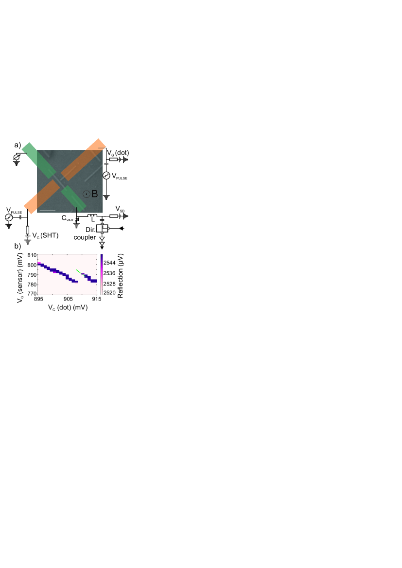
The device used in this study consists of a QD formed at the end of a Ge HW and a charge sensor capacitively and tunnel coupled to it, which is used both as a hole reservoir and for the spin readout 25. The charge sensor is a single hole transistor (SHT), formed in a HW which grows perpendicular to that hosting the spin qubit (Fig. 1a). Whenever a hole tunnels from the QD to the charge sensor a break in the SHT coulomb peak appears (Fig. 1b). In the presence of an external magnetic field, such a single hole tunnelling event becomes spin selective. In order to detect it, the Zeeman splitting, must be larger than the width of the Fermi distribution of the SHT states; where g denotes the g-factor, the Bohr magneton and B the applied magnetic field.
For performing single-shot measurements with high bandwidth, we used a reflectometry-based readout setup, where the SHT is part of the resonant circuit 26, 27, 28, 29, 30. A radio frequency (RF) wave is sent towards the SHT and each change in its impedance manifests as a change in the amplitude of the reflected wave. All measurements were performed in a dilution refrigerator with a base temperature of 15 mK.
2 Results
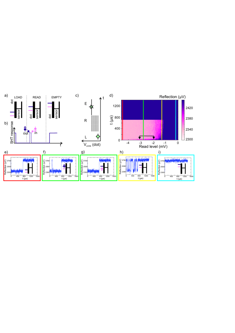
For the spin readout measurement we use the already well established three-stage pulsing sequence (Fig. 2a) implemented by Elzerman et al. 7 to do spin-to-charge conversion. In a first stage (load), a hole with an unknown spin is loaded from the sensor into the dot. In a second stage (read), the electrochemical potentials of the QD for spin up () and spin down () are brought in a configuration where is above and below the electrochemical potential of the SHT (). With the last pulse (empty), the loaded hole tunnels out of the QD. The charge sensor, SHT, shows maximum (minimum) reflection amplitude (RA) when the QD is empty (loaded) (Fig. 2b). In the read phase one distinguishes between two cases, depending on whether a spin up or spin down hole has been loaded. In case a spin down hole is loaded, the SHT RA stays at its minimum during the read stage. However, when a spin up hole is loaded it can tunnel out of the QD. As a consequence the SHT RA obtains its maximum value until it switches back to the minimum value when the QD gets refilled with a spin down hole.
For determining, in the first place, the correct position of the read level for which spin dependent tunnelling is occurring, a similar three-stage sequence was applied (Fig. 2c), with the difference that the amplitude of the read stage was varied. Averaging about 200 single-shot measurements reveals the spin signature (Fig. 2d) as a purple tail at the beginning of the read phase between roughly -3 mV and -2 mV (black double arrow in Fig. 2d). Different RA responses of the SHT are observed depending on the position of the read level, starting from too low (Fig. 2e) to too high (Fig. 2i). The green line in Fig. 2d is positioned such that . Two single-shot measurements taken at the position of the green line are shown in Fig. 2f) and Fig. 2g). Fig. 2f corresponds to a loaded spin up hole, while Fig. 2g to a spin down hole. For the neighbouring break of the same Coulomb peak we do not see the spin signature, as this method works only when the QD has an even number of holes before the load stage. We note that in our measurements we could not see the existence of discrete energy levels in the SHT.
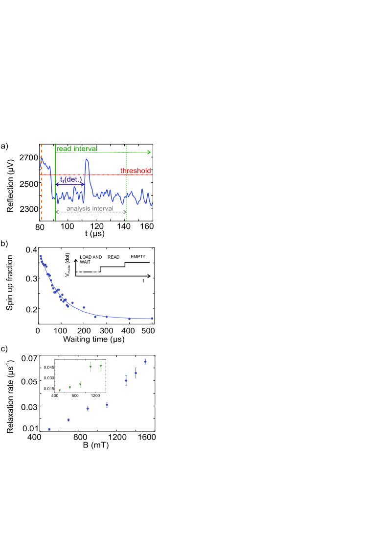
Once the correct position of the read level was determined, the sequence for spin readout was applied (Fig. 3b, inset). In order to extract the hole spin relaxation time, the duration of the first, load stage of the pulse, is varied, while the durations of the read and empty stages are kept constant. The probability of observing a spin-up hole decreases exponentially with the waiting time. From the exponential decay, we extract a hole spin relaxation time of s for out-of-plane magnetic fields of 500 mT (Fig. 3b). As expected, the spin relaxation rate increases when increasing the magnetic field (Fig. 3c). We note that the values extracted from the single-shot measurements are in agreement with those extracted by integrating the averaged RA 31.
3 Discussion
The magnetic field dependence of does not follow a curve (Fig. 3c) which has been shown for electrons in GaAs and Si 1, 8, 9. For holes the Bir-Pikus Hamiltonian which describes the strain in the valence band needs to be considered 32. As it contains strain tensor elements and the spin operators 19 it leads to a hole-phonon Hamiltonian which depends both on the spin and the phonons. This is different from the conduction band where the electron-phonon interaction does not depend on the spin. By taking the Bir-Pikus Hamiltonian into account a hole spin relaxation rate dependence has been recently predicted for Ge/Si core/shell nanowires 33. However, the experimental data reveal a for the first break and a dependence of the spin relaxation rate 31 which is deviating from what was predicted from theory for cylindrical nanowires.
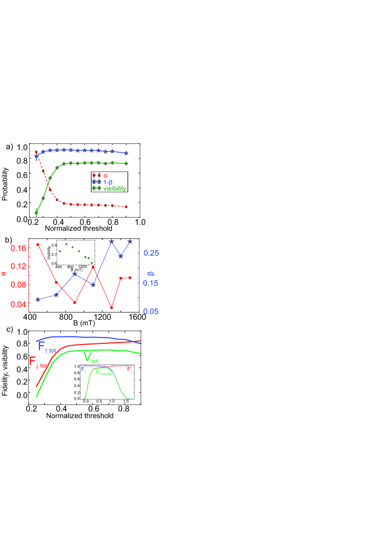
To estimate the accuracy of the single-shot spin readout measurements, we followed a hybrid approach based on the methods introduced by Elzerman et al. 7 and Morello et al. 8. This approach allowed us to get insight in the limitations of hole spins as potential qubits. Initially we extracted the spin-to-charge conversion fidelities. For each threshold used in the single-shot analysis, we extracted two parameters, and . Both correspond to a wrong assignment of the spin states. The parameter gives the probability that the SHT signal exceeds the threshold even in the case of loading a spin down hole, and can be extracted from the saturation value of the spin up fraction for very long waiting times (Fig. 3b). The parameter corresponds to the probability that a spin up hole relaxes before it tunnels out. It is equal to 1/(1 + ), where is the spin up tunnel rate. From the fit to the histogram representing the detection times of the spin up hole (t↑(det) in Fig. 3a), one can extract the decay rate equal to , which then allows the extraction of 31. Due to the large setup bandwidth, is largely threshold insensitive as shown in Fig. 4a) for 500 mT. The spin-to-charge conversion fidelity for the spin down hole (1-) is 0.833 0.005 while for the spin up hole (1-) it is 0.907 0.007, giving a maximum spin-to-charge conversion visibility (1- - ) of 0.740 0.009 for the normalized threshold of 0.7 (Fig. 4a).
In order to get a better understanding into the factors limiting the spin-to-charge conversion fidelities for holes, the dependence of and on the magnetic field was investigated (Fig. 4b). While tends to decrease for larger magnetic fields, shows the opposite behaviour. This leads to a maximum total spin-to-charge conversion visibility of 0.81 0.01 at 700 mT. implies mainly a failure of the spin down hole to remain in the QD. The tunnel out time of the spin down state and thus 1- depends on the ratio of the magnetic field and the effective electron temperature (EET) 9. One solution for increasing 1- is to increase the magnetic field. However, larger magnetic fields imply short spin relaxation times and large qubit operation frequencies. The optimal solution is to keep the magnetic field at low values and decrease the effective electron temperature. Since the reported experiment was performed at an EET of about 300-400 mK 31, fidelities 1- higher than 0.95 should be feasible at magnetic fields of about 200 mT for an EET of 100 mK. We now turn our attention to . As is rather insensitive to the magnetic field 31, the increase of originates from the drastically reduced spin relaxation times. Taking into account the dependence of the spin relaxation rate, relaxation times exceeding 0.3 ms should be feasible at 200 mT. This is in line with the values reported for core-shell wires at low magnetic fields 13. Such longer spin relaxation times will allow 1- to exceed 0.95. From the above discussion it becomes clear that the main difference of hole spins compared to electron spins lays in . While for electron spins is as well limited by the magnetic field value 9, this is not the case for . For electron spins the spin relaxation time is in the order of seconds even at fields exceeding 1 T 8, 9, which in combination with the short tunnelling times makes rather insensitive to the value of the magnetic field.
We now move to the charge readout fidelity. For this we performed a simulation following the procedure introduced by Morello et al. 8, 31. Spin down and spin up fidelities of 0.962 and 0.980 were obtained (Fig. 4c, inset). These fidelities are as high as those reported for electron spins as for the charge readout fidelities it is the measurement bandwidth which determines the extracted values. Finally, in order to obtain the total spin up and spin down fidelities and visibility of the single-shot measurements, the spin-to-charge conversion and charge readout fidelities were multiplied (Fig. 4c). The total spin down (up) hole fidelity is given by 0.801 0.005 (0.889 0.007) and the total visibility of the single shot readout measurements is 0.691 0.008. These values correspond to the normalized threshold of 0.7. By repeating the same analysis for 700 mT a total visibility of 0.752 0.009 was obtained 31.
In summary, as the interest in hole spin qubits 10, 12 has been continuously increasing over the past few years 34, 35, 36, 37, the demonstration of hole spin readout in single QD devices is an important first step towards more complex geometries 38, 39, 40. The reported spin-to-charge conversion and charge readout out fidelities suggest that hole devices operated at low magnetic fields can lead to qubits with spin readout fidelities exceeding 0.9. The reported results together with the CMOS compatibility, the possibility of isotopical purification and the strong spin orbit coupling, suggest Ge as a promising material system for moving towards long range coupling and spin entanglement 41, 42.
4 Methods
The Ge HWs used in this study were grown by a solid-source molecular beam epitaxy (MBE) system on 4-inch intrinsic Si(001) wafers via the Stranski-Krastanow growth mechanism. The wafers were dipped in a hydrofluoric solution before loading into the MBE chamber. After degassing at 720 ∘C, a Si buffer layer was deposited. Then, 6.6 Å of Ge were deposited on the substrate at 580 ∘C followed by an in-situ annealing of 5h at 570 ∘C . The amount of the deposited Ge is at the critical thickness for the nucleation of three dimensional hut clusters. At last, the temperature was decreased to 300 ∘C and the samples were capped with 4 nm of Si.
Electrical contacts on the wires were fabricated by means of electron-beam lithography and electron-beam metal evaporation. For the source and the drain electrodes a combination of Al/Pd was used (7 nm/27 nm). Before the metal deposition, a short dip in buffered hydrofluoric acid was performed in order to remove the native oxide. For the gate electrodes Ti/Pd (5/20 nm) were deposited on top of 8 nm hafnium oxide created by atomic layer deposition.
All measurements were performed in a dilution refrigerator with a base temperature of 15 mK. A Tektronix AWG5014C arbitrary wave generator was used to apply voltage pulses to the gates and the Zurich Instruments UHFLI lock-in amplifier was used for the readout. The sample was mounted onto a printed circuit board incorporating RC filters (R = 10 k, C = 10 nF) for the DC lines, the bias tees for the reflectometry (R = 10 k, C = 10 nF) and the fast gate lines (R = 1.8 M, C = 10 nF). The matching circuit consisted of an 820 nH inductor (1206CS-821XJLB) and a varactor (MA46H070-1056) which was biased with 3 V. The fast gate and the input reflectometry lines were attenuated by 27 dB and 42 dB, respectively. Attenuators were distributed at the different stages of the dilution refrigerator and at room temperature. The reflected signal was amplified at two stages, once at 4K and once at room temperature. We used a CITLF2 cryogenic amplifier, a ZX60-33LN-S+ room temperature amplifier and a ZX30-9-4-S+ directional coupler. The power of the RF signal on the lock-in output was -35 dBm.
5 Data availability
The data that support the findings of this study are available from the corresponding author upon reasonable request.
6 Acknowledgments
We thank C. Kloeffel, A. Laucht, D. Loss and M. Veldhorst for helpful discussions. The work was supported by the ERC Starting Grant no. 335497, the FWF-Y 715-N30 project and the Austrian Ministry of Science through the HRSM call 2016. This research was supported by the Scientic Service Units of IST Austria through resources provided by the MIBA Machine Shop and the Nanofabrication Facility.
7 Contributions
L.V. performed the measurements and analysed the data under the supervision of G.K. J.K. contributed to the development of the RF parts for the experiment. L.V. fabricated the devices with participation of H.W. and G.K.. H.W. and F.S. were responsible for the growth of the samples. J.M.M. performed the simulation for the charge readout fidelity. L.V. and G.K. designed the experiment and wrote the manuscript with input from all authors
8 Competing Interests
Authors declare no competing interests.
References
- 1 Hanson, R., Kouwenhoven, L. P., Petta, J. R., Tarucha, S. & Vandersypen, L. M. K. Spins in few-electron quantum dots. Rev. Mod. Phys. 79, 217–1265 (2007).
- 2 Zwanenburg, A. et al., Silicon quantum electronics. Rev. Mod. Phys. 85, 961–1019 (2013).
- 3 Muhonen J. T. et al. Storing quantum information for 30 seconds in a nanoelectronic device. Nature Nanotechnology 9, 986–991 (2014).
- 4 Yoneda, J. et al. A quantum-dot spin qubit with coherence limited by charge noise and fidelity higher than 99.9%. Nature Nanotechnology 13, 102–106 (2018).
- 5 DiVincenzo, D. P. The physical implementation of quantum computation. Fortschr. Phys. 48, 771–783 (2000).
- 6 Warburton, R. J. Single spins in self-assembled quantum dots. Nature Materials 12, 483–493 (2013).
- 7 Elzerman, J. M. et al. Single-shot read-out of an individual electron spin in a quantum dot. Nature 430, 431–435 (2004).
- 8 Morello, A. et al. Single-shot readout of an electron spin in silicon. Nature 467, 687–691 (2010).
- 9 Büch, H. Mahapatra, S., Rahman, R. Morello, A. & Simmons, M. Y. Spin readout and addressability of phosphorus-donor clusters in silicon. Nature Comm. 4, 2017 (2013).
- 10 Maurand, R. et al. A cmos silicon spin qubit. Nature Comm. 7, 13575 (2016).
- 11 Prechtel, J. H. et al. Decoupling a hole spin qubit from the nuclear spins.Nature Materials 15 981–986 (2016).
- 12 Watzinger, H. et al. Ge hole spin qubit. Preprint at https://arxiv.org/pdf/1802.00395.pdf (2018).
- 13 Hu, Y., Kuemmeth, F., Lieber, C. M. & Marcus, C. M. Hole spin relaxation in ge-si core-shell nanowire qubits. Nature Nanotechnology 7, 47–50 (2012).
- 14 Gerardot, B. D. et al. Optical pumping of a single hole spin in a quantum dot. Nature 451, 441–444 (2008).
- 15 Heiss, D. et al. Observation of extremely slow hole spin relaxation in self-assembled quantum dots. Phys. Rev. B 76, 241306 (2007).
- 16 Zhang, J. J. et al. Monolithic growth of ultrathin ge nanowires on si(001). Phys. Rev. Lett. 109, 085502 (2012).
- 17 Hao, X.-J. et al. Strong and tunable spin-orbit coupling of one-dimensional holes in ge/si core/shell nanowires. Nano Lett. 10, 2956–2960 (2010).
- 18 Higginbotham, A. P. et al. Antilocalization of coulomb blockade in ge/si nanowire. Phys. Rev. Lett. 112, 216806 (2014).
- 19 Kloeffel, C., Rančić, M. J. & Loss, D. Direct rashba spin-orbit interaction in si and ge nanowires with different growth directions. Preprint at https://arxiv.org/pdf/1712.03476.pdf (2017).
- 20 Schoelkopf, R. J., Wahlgren, P., Kozhevnikov, A. A., Delsing, P. & Prober D. E. The radio-frequency single-electron transistor (rf-set): a fast and ultrasensitive electrometer. Science 280, 1238–1242 (1998).
- 21 Watzinger, H. et al. Heavy-hole states in germanium hut wires. Nano Lett. 16, 6879–6885 (2016).
- 22 Fischer J., Coish, W. A., Bulaev, D. V. & Loss, D. Spin decoherence of a heavy hole coupled to nuclear spins in a quantum dot. Phys. Rev. B 78, 155329 (2008).
- 23 Katsaros, G. et al. Positioning of strained islands by interaction with surface nanogrooves. Phys. Rev. Lett. 101, 096103 (2008).
- 24 Zhang, J. J. et al. SiGe growth on patterned si(001) substrates: surface evolution and evidence of modified island coarsening. Appl. Phys. Lett. 91, 173115 (2007).
- 25 Vukušić, L., Kukučka, J., Watzinger, H. & Katsaros, G. Fast hole tunneling times in germanium hut wires probed by single-shot reflectometry. Nano Lett. 17, 5706–5710 (2017).
- 26 Reilly, D. J., Marcus, C. M., Hanson, M. P. & Gossard, A. C. Fast single-charge sensing with a rf quantum point contact. Appl. Phys. Lett. 91, 162101 (2007).
- 27 Jung, M., Schroer, M. D., Petterson, K. D. & Petta, J. R. Radio frequency charge sensing in inas nanowire double quantum dots. Appl. Phys. Lett. 100, 253508 (2012).
- 28 Frake, J. C. et al. Radio-frequency capacitance spectroscopy of metallic nanoparticles. Scientific Reports 5, 10858 (2015).
- 29 Ares, N. et al. Sensitive radio-frequency measurements of a quantum dot by tuning to perfect impedance matching.Phys. Rev. Applied 5, 034011 (2016).
- 30 Hile, S. J. et al. Radio frequency reflectometry and charge sensing of a precision placed donor in silicon. Appl. Phys. Lett. 107, 093504 (2015).
- 31 Supplementary Information.
- 32 Bir G. L. & Pikus, G. E. Symmetry and Strain-induced Effects in Semiconductors. Wiley, New York, 1974.
- 33 Maier, F., Kloeffel, C. & Loss, D. Tunable g factor and phonon-mediated hole spin relaxation in ge/si nanowire quantum dots. Phys. Rev. B 87, 161305 (2013).
- 34 Hendrickx, N. W. et al. Gate-controlled quantum dots and superconductivity in planar germanium. Preprint at https://arxiv.org/pdf/1801.08869.pdf (2018).
- 35 Brauns, M. et al. Anisotropic pauli spin blockade in hole quantum dots. Phys. Rev. B 94, 041411 (2016).
- 36 Li, R., Hudson, F. E, Dzurak, A. S. & Hamilton, A. R. Pauli spin blockade of heavy holes in a silicon double quantum dot. Nano Lett. 15, 7314–7318 (2015).
- 37 Wang, D. Q. et al. Anisotropic Pauli spin blockade of holes in a GaAs double quantum dot. Nano Lett. 16, 7685–7689 (2016).
- 38 Zajac D. M. et al. Resonantly driven cnot gate for electron spins. Science 359, 439–442 (2018).
- 39 Veldhorst, M. et al. A two-qubit logic gate in silicon. Nature 526, 410–414 (2015).
- 40 Watson, T. F. et al. A programmable two-qubit quantum processor in silicon. Nature 555, 633–637 (2018).
- 41 Nigg, S. E., Fuhrer, A. & Loss, D. Superconducting grid-bus surface code architecture for hole-spin qubits. Phys. Rev. Lett. 118, 147701 (2017).
- 42 Kloeffel, C., Trif, M., Stano, P. & Loss, D. Circuit qed with hole-spin qubits in Ge/Si nanowire quantum dots. Phys. Rev. B 88, 241405 (2013).