Integrated Plasmonics: Broadband Dirac Plasmons in Borophene
Abstract
The past decade has witnessed numerous discoveries of two-dimensional (2D) semimetals and insulators, whereas 2D metals are rarely identified. Borophene, a monolayer boron sheet, has recently emerged as a perfect 2D metal with unique structure and electronic properties. Here we study collective excitations in borophene, which exhibit two major plasmon modes with low damping rates extending from infrared to ultraviolet regime. The anisotropic 1D plasmon originates from electronic excitations of tilted Dirac cones in borophene, analogous to that in heavily doped Dirac semimetals. These features make borophene promising to realize directional polariton transportation and broadband optical communications for next-generation optoelectronic devices.
When propagating along the metal-dielectric interface in plasmonic devices, electromagnetic waves couple with electronic motions and form surface plasmon polaritons (SPPs) Pitarke et al. (2006); Stefan A. Maier (2007). Noble metal films (e.g. Ag and Au) provide abundant free electrons to generate high-frequency plasmons in SPP devices Gao et al. (2011); Thongrattanasiri et al. (2012); Sessi et al. (2015); Zubizarreta et al. (2017). However, the SPPs in these devices suffer from low confinements and significant losses during propagation Sundararaman et al. (2020); Slotman et al. (2018); Rivera et al. (2016), resulted from the manifold interband damping and strong plasmon-phonon scatterings West et al. (2010); Jablan et al. (2009).
Naturally, ultrathin two-dimensional (2D) materials, such as graphene Low and Avouris (2014a); de Abajo (2014a); Shirodkar et al. (2018); Ni et al. (2018), phosphorene Low et al. (2014); Ghosh et al. (2017); Saberi-Pouya et al. (2017); Gomes and Carvalho (2015); van Veen et al. (2018), and MoS2 Scholz et al. (2013); Liu et al. (2016a); Yue et al. (2017); Sen et al. (2017); Liu et al. (2016b); Miao et al. (2015); Torbatian and Asgari (2017), are proposed to generate SPPs with low damping rates and high confinements due to stronger light-matter interactions Sarma and Madhukar (1981); Hwang and Sarma (2007); Yuan and Gao (2008); Dai et al. (2015); Cox et al. (2016); Fei et al. (2012); Polini et al. (2008); Chen et al. (2012); Ansell et al. (2015); de Abajo (2014b); Xia et al. (2014); Thakur et al. (2017); Fang and Sun (2015); Gomez et al. (2016); Marušić and Despoja (2017); Yan et al. (2011a); Despoja and Marušić (2018); Hu et al. (2019). However, low carrier densities in these materials limit the frequencies of the plasmonic response up to terahertz or infrared region, where light sources and optoelectronic detectors are less developed Gao and Yuan (2011); Koppens et al. (2011); Low and Avouris (2014b); Low et al. (2016); Brar et al. (2013, 2014); Ni et al. (2016). The 2D materials with higher carrier density and higher plasmon frequencies are particularly desirable for building optical devices with beyond-diffraction-limit resolutions, detecting biotechnological processes, and enhancing atomic transitions Gérard and Gray (2014); Soukoulis and Wegener (2011); Pendry (2000).
Recently, borophene, a monolayer boron sheet, has been experimentally synthesized either on a solid substrate via molecular beam epitaxy Mannix et al. (2015); Feng et al. (2016a) or as free-standing atomic sheets via sonochemical liquid-phase exfoliation Ranjan et al. (2019a). Borophene has extraordinary electric, optical and transport properties which are highly related to its intrinsic metallic, Dirac-type band structures Feng et al. (2017a, b); Zhang et al. (2018); Feng et al. (2016b); Zhao et al. (2016); Penev et al. (2016); Jalali-Mola and Jafari (2018); Huang et al. (2017). The density of the Dirac electrons in borophene is extremely high ( /cm2) Feng et al. (2017a, b); Zhang et al. (2018) compared to doped graphene ( /cm2) Efetov and Kim (2010). Thus, we expect that borophene, as an intrinsic 2D metal with both high carrier densities and high confinements, can be a promising candidate to build low-loss broadband SPP devices.

In this work, we report discovery of low-loss and highly-confined broadband plasmons in borophene, based on time-dependent density functional theory (TDDFT) 111The frequency and wavevector dependent density response functions are calculated within the TDDFT formalism using random phase approximation as implemented in the GPAW package Mortensen et al. (2005); Enkovaara et al. (2010); Yan et al. (2011b); Larsen et al. (2017); Bahn and Jacobsen (2002). The projector augmented-waves method and Perdew-Burke-Ernzerhof exchange-correlation Perdew et al. (1996) are used for the ground state calculations. The plane-wave cutoff energy is set to be 500 eV. The thickness of vacuum layer is set to be larger than 10 Å. The Brillouin zone is sampled using the Monkhorst-Pack scheme Monkhorst and Pack (1976) with a dense k-point mesh in the self-consistent calculations.. In our calculations, we observe two plasmon branches: A high energy (HE) mode extends to ultraviolet and originates from collective excitations of bulk electrons in the 2D material; in the low energy (LE) region, a new plasmon mode exhibits a strong anisotropic behavior and broadband response. The new plasmon mode originates from collective electronic transitions of one-dimensional (1D) electron gas derived from tilted Dirac cones. Both modes show remarkable low-loss properties comparable to graphene, but at significant higher frequencies, thanks to borophene’s high carrier density and low-dimensional nature Jablan et al. (2009). The confinement of plasmon in borophene is also 2-3 orders of magnitude higher than that in Ag Sundararaman et al. (2018). The discovery of novel plasmon modes make borophene more suitable than graphene and noble metals for plasmon generation and integrated optoelectronics working at a broad range of frequencies.
Figure 1 shows the atomic structure of the borophene. The borophene is the most stable phase found in experiments Mannix et al. (2015); Feng et al. (2016a); Ranjan et al. (2019a) and is thus chosen as a representative structure of borophene. The unit cell is rectangular with the lattice parameters Å and Å, consisting of five boron atoms. Periodic vacancies line up along the horizontal direction (denoted as the X direction). This special structure introduces anisotropy between the horizontal (X) and vertical (Y) directions in both the real and reciprocal space [Fig. 1(a)].
The optical absorption spectra, obtained from the imaginary parts of the dielectric functions, are shown in Fig. 1(b-c). We observe two plasmon branches in different broad energy ranges in our calculations. A high energy branch (HE mode) disperses almost linearly and extends to the ultraviolet regime ( eV) at the momentum range Å-1. This mode is almost isotropic along the X and Y directions. In contrast, a low energy branch (LE mode) shows evidently anisotropic dispersions along different directions. Along the -X direction, the LE branch shows an inverted parabolic dispersion over the whole Brillouin zone, with the maximum energy at the half of the reciprocal lattice vector, Å-1. Along the -Y, however, only the HE mode shows up at small regimes; the LE mode develops only at energies higher than 2 eV, whereas the two plasmon modes strongly hybridize with each other. The features are significantly different from the behaviors along the -X direction.
Both the HE and LE branches can form a broadband SPP with low losses. As shown in Fig. 1(d) and (e), we calculate the confinement ratio and relative loss of borophene plasmons, where and are the light wavelengths in air and borophene, respectively Jablan et al. (2009). The LE plasmons possess high confinement ratios of 330–700 and long losses of 10–700 at different wavelengths from 400 to 1240 nm. The and of the HE plasmon are slightly lower over a broader energy range. Both the confinement ratios and losses are comparable to those in heavily doped graphene ( and ) Jablan et al. (2009) and much larger than those in the Al or Ag films () Sundararaman et al. (2018). Furthermore, the low damping SPPs only exists within the infrared regime ( nm) in graphene Jablan et al. (2009); Shirodkar et al. (2018); Torbatian and Asgari (2017); Ghosh et al. (2017), while borophene can generate the low-loss SPPs in a much broader energy range from infrared to ultraviolet. This indicates that borophene is a better building material for the low-loss broadband optoelectronic devices.
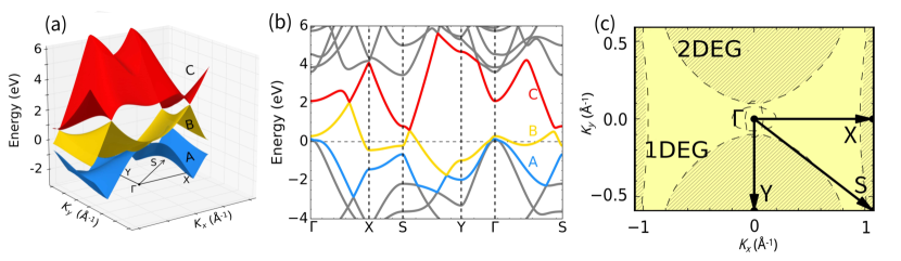
In the following paragraphs, we discuss the electronic origin of these two outstanding characteristics, the anisotropy and low-loss rate, of the borophene plasmon. We first note that the anisotropic plasmon in borophene is not a trivial consequence of the rectangular lattice, which generates only a weak anisotropy in phosphorene plasmons Ghosh et al. (2017). Instead, the unique electronic structure is the major reason of the anisotropy. As shown in Fig. 2(a) and (b), band B crosses the Fermi energy and joins band C at the Dirac points at 2 eV, indicating the metallic nature of borophene and forming the Fermi surface, as shown in Figure 2(c). Another Dirac point forms along the S–Y direction and at a lower energy, 0.5 eV. Both Dirac cones are tilted in their shape, consistent with experimental measurements Feng et al. (2017a, b). Thus, borophene forms a Fermi surface comprising three parts: (I) a ribbon along -Y centered at X, implying a 1D electron gas (1DEG) from tilted Dirac electrons subjecting to strong confinement along the Y direction; (II) two semicircular regions characterizing a bulk 2D electron gas; (III) a small hole pocket near the point.
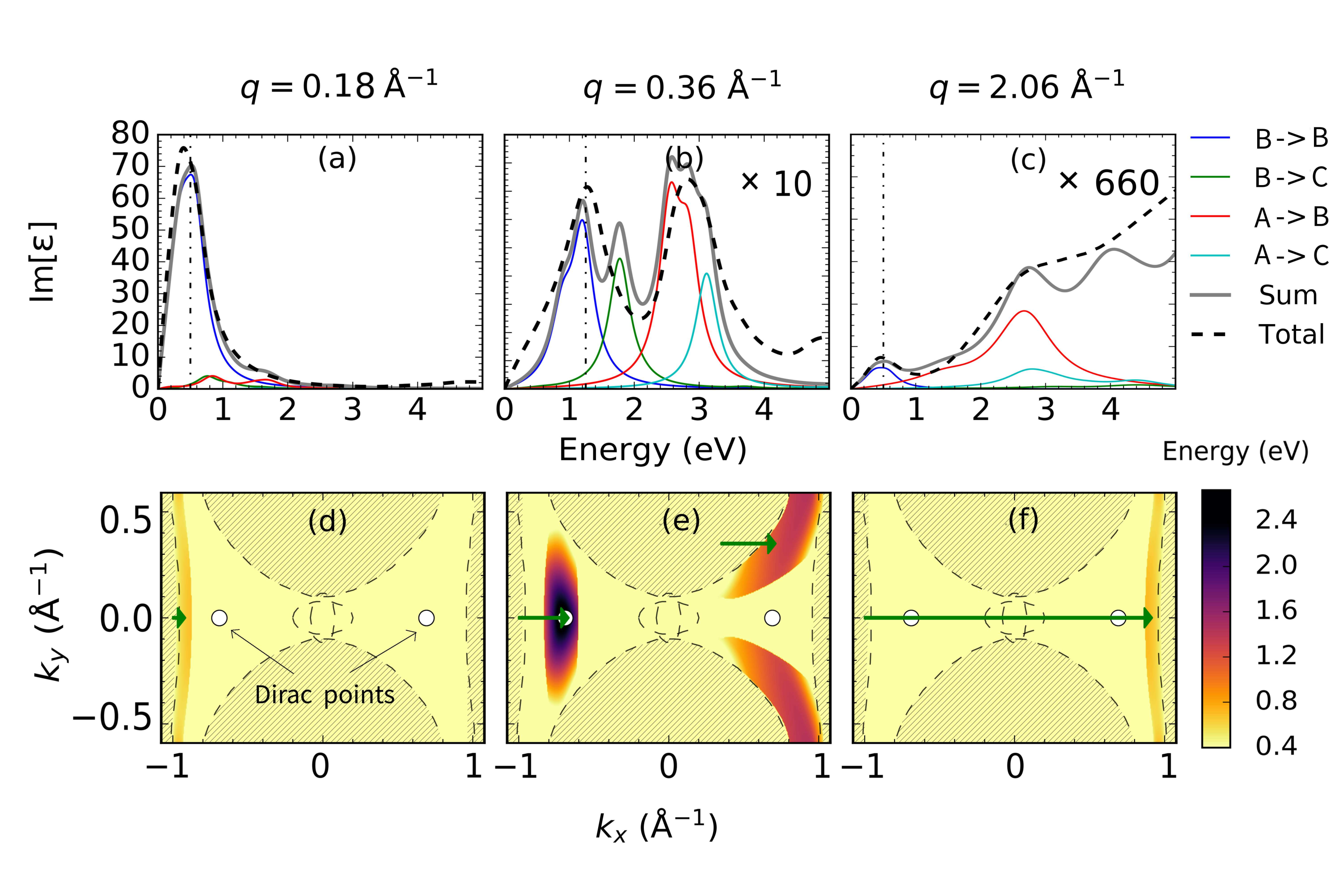
We ascribe the anisotropic LE mode to the intraband oscillations of the 1DEG between the Dirac cones. As shown in Fig. 3, we analyze the contributions of different electron-hole transitions to the plasmonic peaks within the independent particle approximation (IPA). As shown in Fig. 3(a-c), the HE mode emerges mainly at eV for Å-1, which comes from mixed interband transitions of band A B, band A C and band B C. In comparison, the LE peaks are located at 1.08, 1.79, and 0.5 eV for , 0.36, and 2.06 Å-1, respectively, which are dominated by the intraband transitions B B. Accordingly, we visualize the excitation mode of the LE plasmon in the reciprocal space. The contour plot of the energy difference, , between the initial state and final state , where for , is the eigenvalue of band B at the point. As shown in Fig. 3(d-f), the oscillation of the 1DEG dominates the LE mode and leads to its anisotropy, since the 1DEG can only oscillate along -X direction. Specifically, at Å-1, the LE plasmon is generated by electron excitations from the Fermi surface to the Dirac points Feng et al. (2017a). Thus, borophene can be viewed as an extremely hole-doped graphene in generating the LE plasmon.
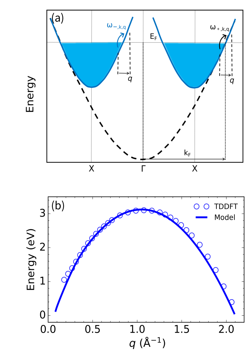
To explain the mechanism of the low-damping characteristic, we adopt the confined 1DEG model Sarma and Hwang (1996); Gao and Yuan (2005); Yan et al. (2007) that is widely used to describe plasmons of atomic chains Ritsko et al. (1975); Rugeramigabo et al. (2010); Nagao et al. (2006); Yan and Gao (2008); Liu et al. (2008a, b). We find an additional excitation channel exists in the borophene for its special 1DEG centered at X point (1DEG@X), compared with the usual 1DEG@: For excitations at certain momentum , the conventional channel for 1DEG@ [the black arrow in Fig. 4(a)] is , with (assuming and is the effective mass of electron). For 1DEG@X, there is an additional channel (the blue arrow) located on the opposite side () .
Accordingly, we calculate the plasmon dispersions of these two excitation channels, which are determined from the zeros of the dielectric function . Here, is the frequency of plasmom, is the Coulomb potential, is the response function with IPA Friesen and Bergersen (1980) . Thus, , where are the upper (+) and lower (–) limits of the single-particle excitation (SPE) regimes, respectively. The 1D plasmon dispersions can be solved as and Sarma and Hwang (1996); Friesen and Bergersen (1980), where , , is the static dielectric constant, is the width of the 1DEG, and is the effective mass of electrons the 1DEG.
As shown in Fig. 4(b), while hybridizes and merges with the isotropic HE mode, accurately reproduces the inverse parabolic dispersion calculated from TDDFT, with the parameters Å-1, 4 Å, and . We note that, among the parameters, is the length of -X and thus not adjustable; 1DEG width and dielectric constant have negligible effects on when Å-1. The effective mass is slightly larger than that evaluated from the band structure , due to many body screening effects. This indicates that our model directly and robustly reflects the electronic origin of novel borophene plasmon.
The same model may also explain the LE plamon branch along the -Y direction. Along -Y, electrons first undergo an interband excitation to energy levels at 2 eV above the Fermi level, where electrons form a similar 1DEG confined along -Y direction. With strong interband transitions included in plasmon excitations, excitations of the 1DEG at -Y have similar excitation channels as 1DEG along -X discussed above. Therefore, a kink in plasmon dispersion at 2 eV is formed, followed by an inverse parabolic dispersion along the -Y direction.
Based on these results, we discuss the mechanism of the low-damping behavior of the LE plasmon. With , these two branches and yield different asymptotic behaviors. The dominates when and leads and . That is, [] is always higher (lower) than the SPE region. Moreover, the Dirac-type intraband excitations [Fig. 3(e)] further suppress the SPE region, since the pseudospin symmetry forbids perpendicularly-polarized excitations Hwang and Sarma (2007). The combined effects remarkably produce the low-loss LE plasmons.
We briefly discuss the technical requirements of building realistic plasmonic devices with borophene. The first important requirement is the stability of borophene under ambient conditions. Feng et al. showed that borophene on the Ag substrate is generally robust to the oxidation Feng et al. (2016a). Recently, Ranjan et al. synthesized large-scale free-standing borophene by liquid-phase exfoliation Ranjan et al. (2019b). They claimed that the free-standing borophene layer is even more stable against oxidation. This indicates that a borophene-based device is applicable under ambient conditions.
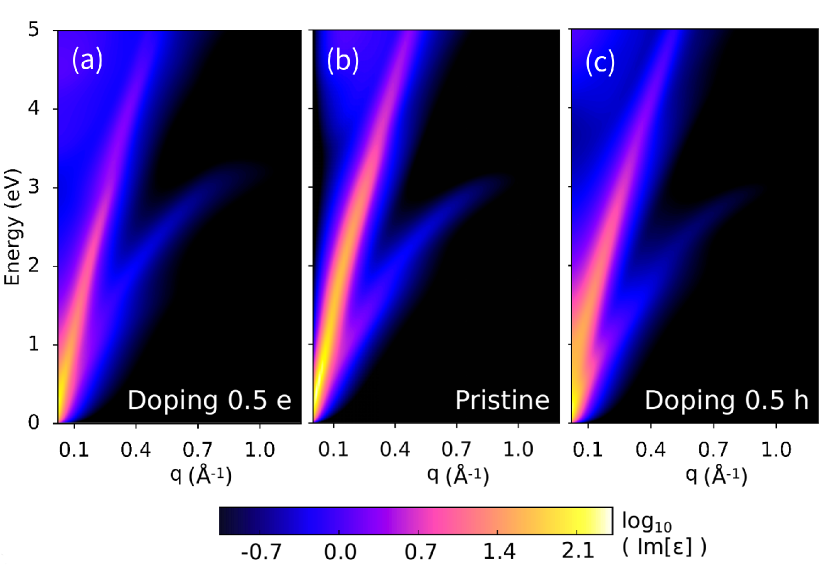
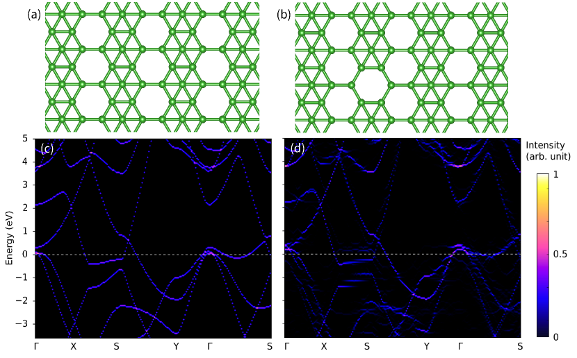
Other than the stability, the plasmonic application requires large-scale high-quality borophene. The point defect in borophene barely affects its band structures [Fig. S4]. Furthermore, the charge doping has little effect on the plasmonic response in borophene, as shown in Fig. S3. Thus, the borophene plasmon is insensitive to a small number of point defects, similar to the experimental observation in graphene Politano et al. (2011); Langer et al. (2010). However, the anisotropic plasmon will probably be substantially smeared in polycrystalline borophene. Synthesis of centimeter-scale single-crystalline borophene is needed for the plasmonic device, which is quite promising considering the achievements in the growth of wafer-scale graphene Lee et al. (2010); Lin et al. (2011), transition metal dichalcogenides Liu et al. , and boron nitride Wang et al. (2019). We hope that the unique plasmon properties predicted in our work could motivate the technical progress in preparing a high-quality borophene sample for building the potential plasmonic devices.
Absent in other 2D materials, we observe in our calculations the coexistence and interplay of the 1DEG, 2DEG and Dirac electrons in the collective plasmon excitations in metallic borophene.
The exotic features such as low-loss, strong confinement and panchromatic responses of LE and HE plasmons make borophene a promising candidate for applications in nanophotonics and integrated optoelectronics working at broadband frequencies.
We acknowledge insightful discussions with Prof. Ling Lu. This work is partially supported by MOST (grants 2016YFA0300902 and 2015CB921001), NSFC (grant 11774396 and 91850120), and CAS (XDB07030100). S.G. acknowledges supports from MOST through grants 2017YFA0303404 and 2016YFB0700701, NSFC through grant NSAF U-1530401.
C.L. and S.H. contribute equally to this work.
References
- Pitarke et al. (2006) J. M. Pitarke, V. M. Silkin, E. V. Chulkov, and P. M. Echenique, Reports on Progress in Physics 70, 1 (2006).
- Stefan A. Maier (2007) Stefan A. Maier, Plasmonics: Fundamentals and Applications (Springer US, 2007).
- Gao et al. (2011) Y. Gao, Z. Yuan, and S. Gao, The Journal of Chemical Physics 134, 134702 (2011).
- Thongrattanasiri et al. (2012) S. Thongrattanasiri, A. Manjavacas, and F. J. G. de Abajo, ACS Nano 6, 1766 (2012).
- Sessi et al. (2015) P. Sessi, V. M. Silkin, I. A. Nechaev, T. Bathon, L. El-Kareh, E. V. Chulkov, P. M. Echenique, and M. Bode, Nature Communications 6, 8691 (2015).
- Zubizarreta et al. (2017) X. Zubizarreta, E. V. Chulkov, I. P. Chernov, A. S. Vasenko, I. Aldazabal, and V. M. Silkin, Physical Review B 95, 235405 (2017).
- Sundararaman et al. (2020) R. Sundararaman, T. Christensen, Y. Ping, N. Rivera, J. D. Joannopoulos, M. Soljačić, and P. Narang, Physical Review Materials 4, 074011 (2020).
- Slotman et al. (2018) G. Slotman, A. Rudenko, E. van Veen, M. I. Katsnelson, R. Roldán, and S. Yuan, Physical Review B 98, 155411 (2018).
- Rivera et al. (2016) N. Rivera, I. Kaminer, B. Zhen, J. D. Joannopoulos, and M. Soljačić, Science 353, 263 (2016).
- West et al. (2010) P. West, S. Ishii, G. Naik, N. Emani, V. Shalaev, and A. Boltasseva, Laser & Photonics Reviews 4, 795 (2010).
- Jablan et al. (2009) M. Jablan, H. Buljan, and M. Soljačić, Physical Review B 80, 245435 (2009).
- Low and Avouris (2014a) T. Low and P. Avouris, ACS Nano 8, 1086 (2014a).
- de Abajo (2014a) F. J. G. de Abajo, ACS Photonics 1, 135 (2014a).
- Shirodkar et al. (2018) S. N. Shirodkar, M. Mattheakis, P. Cazeaux, P. Narang, M. Soljačić, and E. Kaxiras, Physical Review B 97, 195435 (2018).
- Ni et al. (2018) G. X. Ni, A. S. McLeod, Z. Sun, L. Wang, L. Xiong, K. W. Post, S. S. Sunku, B.-Y. Jiang, J. Hone, C. R. Dean, M. M. Fogler, and D. N. Basov, Nature 557, 530 (2018).
- Low et al. (2014) T. Low, R. Roldán, H. Wang, F. Xia, P. Avouris, L. M. Moreno, and F. Guinea, Physical Review Letters 113, 106802 (2014).
- Ghosh et al. (2017) B. Ghosh, P. Kumar, A. Thakur, Y. S. Chauhan, S. Bhowmick, and A. Agarwal, Physical Review B 96, 035422 (2017).
- Saberi-Pouya et al. (2017) S. Saberi-Pouya, T. Vazifehshenas, T. Salavati-fard, and M. Farmanbar, Physical Review B 96, 115402 (2017).
- Gomes and Carvalho (2015) L. C. Gomes and A. Carvalho, Physical Review B 92, 085406 (2015).
- van Veen et al. (2018) E. van Veen, A. Nemilentsau, A. Kumar, R. Roldán, M. I. Katsnelson, T. Low, and S. Yuan, arxiv:1812.03062 (2018).
- Scholz et al. (2013) A. Scholz, T. Stauber, and J. Schliemann, Physical Review B 88, 035135 (2013).
- Liu et al. (2016a) W. Liu, B. Lee, C. H. Naylor, H.-S. Ee, J. Park, A. T. C. Johnson, and R. Agarwal, Nano Letters 16, 1262 (2016a).
- Yue et al. (2017) B. Yue, F. Hong, K.-D. Tsuei, N. Hiraoka, Y.-H. Wu, V. M. Silkin, B. Chen, and H. kwang Mao, Physical Review B 96, 125118 (2017).
- Sen et al. (2017) H. S. Sen, L. Xian, F. H. da Jornada, S. G. Louie, and A. Rubio, Israel Journal of Chemistry 57, 540 (2017).
- Liu et al. (2016b) W. Liu, B. Lee, C. H. Naylor, H.-S. Ee, J. Park, A. T. C. Johnson, and R. Agarwal, Nano Letters 16, 1262 (2016b).
- Miao et al. (2015) J. Miao, W. Hu, Y. Jing, W. Luo, L. Liao, A. Pan, S. Wu, J. Cheng, X. Chen, and W. Lu, Small 11, 2392 (2015).
- Torbatian and Asgari (2017) Z. Torbatian and R. Asgari, Journal of Physics: Condensed Matter 29, 465701 (2017).
- Sarma and Madhukar (1981) S. D. Sarma and A. Madhukar, Physical Review B 23, 805 (1981).
- Hwang and Sarma (2007) E. H. Hwang and S. D. Sarma, Physical Review B 75, 205418 (2007).
- Yuan and Gao (2008) Z. Yuan and S. Gao, Surface Science 602, 460 (2008).
- Dai et al. (2015) S. Dai, Q. Ma, M. K. Liu, T. Andersen, Z. Fei, M. D. Goldflam, M. Wagner, K. Watanabe, T. Taniguchi, M. Thiemens, F. Keilmann, G. C. A. M. Janssen, S.-E. Zhu, P. Jarillo-Herrero, M. M. Fogler, and D. N. Basov, Nature Nanotechnology 10, 682 (2015).
- Cox et al. (2016) J. D. Cox, I. Silveiro, and F. J. G. de Abajo, ACS Nano 10, 1995 (2016).
- Fei et al. (2012) Z. Fei, A. S. Rodin, G. O. Andreev, W. Bao, A. S. McLeod, M. Wagner, L. M. Zhang, Z. Zhao, M. Thiemens, G. Dominguez, M. M. Fogler, A. H. C. Neto, C. N. Lau, F. Keilmann, and D. N. Basov, Nature 487, 82 (2012).
- Polini et al. (2008) M. Polini, R. Asgari, G. Borghi, Y. Barlas, T. Pereg-Barnea, and A. H. MacDonald, Physical Review B 77, 081411 (2008).
- Chen et al. (2012) J. Chen, M. Badioli, P. Alonso-González, S. Thongrattanasiri, F. Huth, J. Osmond, M. Spasenović, A. Centeno, A. Pesquera, P. Godignon, A. Z. Elorza, N. Camara, F. J. G. de Abajo, R. Hillenbrand, and F. H. L. Koppens, Nature 487, 77 (2012).
- Ansell et al. (2015) D. Ansell, I. P. Radko, Z. Han, F. J. Rodriguez, S. I. Bozhevolnyi, and A. N. Grigorenko, Nature Communications 6, 8846 (2015).
- de Abajo (2014b) F. J. G. de Abajo, ACS Photonics 1, 135 (2014b).
- Xia et al. (2014) F. Xia, H. Wang, D. Xiao, M. Dubey, and A. Ramasubramaniam, Nature Photonics 8, 899 (2014).
- Thakur et al. (2017) A. Thakur, R. Sachdeva, and A. Agarwal, Journal of Physics: Condensed Matter 29, 105701 (2017).
- Fang and Sun (2015) Y. Fang and M. Sun, Light: Science & Applications 4, e294 (2015).
- Gomez et al. (2016) C. V. Gomez, M. Pisarra, M. Gravina, J. Pitarke, and A. Sindona, Physical Review Letters 117, 116801 (2016).
- Marušić and Despoja (2017) L. Marušić and V. Despoja, Physical Review B 95, 201408 (2017).
- Yan et al. (2011a) J. Yan, K. W. Jacobsen, and K. S. Thygesen, Physical Review B 84, 235430 (2011a).
- Despoja and Marušić (2018) V. Despoja and L. Marušić, Physical Review B 97, 205426 (2018).
- Hu et al. (2019) H. Hu, X. Yang, X. Guo, K. Khaliji, S. R. Biswas, F. J. García de Abajo, T. Low, Z. Sun, and Q. Dai, Nature Communications 10, 1131 (2019).
- Gao and Yuan (2011) Y. Gao and Z. Yuan, Solid State Communications 151, 1009 (2011).
- Koppens et al. (2011) F. H. L. Koppens, D. E. Chang, and F. J. G. de Abajo, Nano Letters 11, 3370 (2011).
- Low and Avouris (2014b) T. Low and P. Avouris, ACS Nano 8, 1086 (2014b).
- Low et al. (2016) T. Low, A. Chaves, J. D. Caldwell, A. Kumar, N. X. Fang, P. Avouris, T. F. Heinz, F. Guinea, L. Martin-Moreno, and F. Koppens, Nature Materials 16, 182 (2016).
- Brar et al. (2013) V. W. Brar, M. S. Jang, M. Sherrott, J. J. Lopez, and H. A. Atwater, Nano Letters 13, 2541 (2013).
- Brar et al. (2014) V. W. Brar, M. S. Jang, M. Sherrott, S. Kim, J. J. Lopez, L. B. Kim, M. Choi, and H. Atwater, Nano Letters 14, 3876 (2014).
- Ni et al. (2016) G. X. Ni, L. Wang, M. D. Goldflam, M. Wagner, Z. Fei, A. S. McLeod, M. K. Liu, F. Keilmann, B. Özyilmaz, A. H. C. Neto, J. Hone, M. M. Fogler, and D. N. Basov, Nature Photonics 10, 244 (2016).
- Gérard and Gray (2014) D. Gérard and S. K. Gray, Journal of Physics D: Applied Physics 48, 184001 (2014).
- Soukoulis and Wegener (2011) C. M. Soukoulis and M. Wegener, Nature Photonics 5, 523 (2011).
- Pendry (2000) J. B. Pendry, Physical Review Letters 85, 3966 (2000).
- Mannix et al. (2015) A. J. Mannix, X.-F. Zhou, B. Kiraly, J. D. Wood, D. Alducin, B. D. Myers, X. Liu, B. L. Fisher, U. Santiago, J. R. Guest, M. J. Yacaman, A. Ponce, A. R. Oganov, M. C. Hersam, and N. P. Guisinger, Science 350, 1513 (2015).
- Feng et al. (2016a) B. Feng, J. Zhang, Q. Zhong, W. Li, S. Li, H. Li, P. Cheng, S. Meng, L. Chen, and K. Wu, Nature Chemistry 8, 563 (2016a).
- Ranjan et al. (2019a) P. Ranjan, T. K. Sahu, R. Bhushan, S. S. Yamijala, D. J. Late, P. Kumar, and A. Vinu, Advanced Materials 31, e1900353 (2019a).
- Feng et al. (2017a) B. Feng, O. Sugino, R.-Y. Liu, J. Zhang, R. Yukawa, M. Kawamura, T. Iimori, H. Kim, Y. Hasegawa, H. Li, L. Chen, K. Wu, H. Kumigashira, F. Komori, T.-C. Chiang, S. Meng, and I. Matsuda, Physical Review Letters 118, 096401 (2017a).
- Feng et al. (2017b) B. Feng, J. Zhang, S. Ito, M. Arita, C. Cheng, L. Chen, K. Wu, F. Komori, O. Sugino, K. Miyamoto, T. Okuda, S. Meng, and I. Matsuda, Advanced Materials 30, 1704025 (2017b).
- Zhang et al. (2018) J. Zhang, J. Zhang, L. Zhou, C. Cheng, C. Lian, J. Liu, S. Tretiak, J. Lischner, F. Giustino, and S. Meng, ANGEWANDTE CHEMIE-INTERNATIONAL EDITION 57, 4585 (2018).
- Feng et al. (2016b) B. Feng, J. Zhang, R.-Y. Liu, T. Iimori, C. Lian, H. Li, L. Chen, K. Wu, S. Meng, F. Komori, and I. Matsuda, Physical Review B 94, 041408 (2016b).
- Zhao et al. (2016) Y. Zhao, S. Zeng, and J. Ni, Applied Physics Letters 108, 242601 (2016).
- Penev et al. (2016) E. S. Penev, A. Kutana, and B. I. Yakobson, Nano Letters 16, 2522 (2016).
- Jalali-Mola and Jafari (2018) Z. Jalali-Mola and S. A. Jafari, Physical Review B 98, 235430 (2018).
- Huang et al. (2017) Y. Huang, S. N. Shirodkar, and B. I. Yakobson, Journal of the American Chemical Society 139, 17181 (2017).
- Efetov and Kim (2010) D. K. Efetov and P. Kim, Phys. Rev. Lett. 105, 256805 (2010).
- Note (1) The frequency and wavevector dependent density response functions are calculated within the TDDFT formalism using random phase approximation as implemented in the GPAW package Mortensen et al. (2005); Enkovaara et al. (2010); Yan et al. (2011b); Larsen et al. (2017); Bahn and Jacobsen (2002). The projector augmented-waves method and Perdew-Burke-Ernzerhof exchange-correlation Perdew et al. (1996) are used for the ground state calculations. The plane-wave cutoff energy is set to be 500 eV. The thickness of vacuum layer is set to be larger than 10 Å. The Brillouin zone is sampled using the Monkhorst-Pack scheme Monkhorst and Pack (1976) with a dense k-point mesh in the self-consistent calculations.
- Sundararaman et al. (2018) R. Sundararaman, T. Christensen, Y. Ping, N. Rivera, J. D. Joannopoulos, M. Soljačić, and P. Narang, arxiv:1806.02672 (2018).
- Sarma and Hwang (1996) S. D. Sarma and E. H. Hwang, Physical Review B 54, 1936 (1996).
- Gao and Yuan (2005) S. Gao and Z. Yuan, Physical Review B 72, 121406 (2005).
- Yan et al. (2007) J. Yan, Z. Yuan, and S. Gao, Physical Review Letters 98, 216602 (2007).
- Ritsko et al. (1975) J. J. Ritsko, D. J. Sandman, A. J. Epstein, P. C. Gibbons, S. E. Schnatterly, and J. Fields, Physical Review Letters 34, 1330 (1975).
- Rugeramigabo et al. (2010) E. P. Rugeramigabo, C. Tegenkamp, H. Pfnür, T. Inaoka, and T. Nagao, Physical Review B 81, 165407 (2010).
- Nagao et al. (2006) T. Nagao, S. Yaginuma, T. Inaoka, and T. Sakurai, Physical Review Letters 97, 116802 (2006).
- Yan and Gao (2008) J. Yan and S. Gao, Physical Review B 78, 235413 (2008).
- Liu et al. (2008a) C. Liu, T. Inaoka, S. Yaginuma, T. Nakayama, M. Aono, and T. Nagao, Physical Review B 77, 205415 (2008a).
- Liu et al. (2008b) C. Liu, T. Inaoka, S. Yaginuma, T. Nakayama, M. Aono, and T. Nagao, Nanotechnology 19, 355204 (2008b).
- Friesen and Bergersen (1980) W. I. Friesen and B. Bergersen, Journal of Physics C: Solid State Physics 13, 6627 (1980).
- Ranjan et al. (2019b) P. Ranjan, T. K. Sahu, R. Bhushan, S. S. Yamijala, D. J. Late, P. Kumar, and A. Vinu, Advanced Materials 31, 1900353 (2019b), https://onlinelibrary.wiley.com/doi/pdf/10.1002/adma.201900353 .
- Politano et al. (2011) A. Politano, A. R. Marino, V. Formoso, D. Farías, R. Miranda, and G. Chiarello, Phys. Rev. B 84, 033401 (2011).
- Langer et al. (2010) T. Langer, J. Baringhaus, H. Pfnür, H. W. Schumacher, and C. Tegenkamp, New Journal of Physics 12, 033017 (2010).
- Lee et al. (2010) Y. Lee, S. Bae, H. Jang, S. Jang, S.-E. Zhu, S. H. Sim, Y. I. Song, B. H. Hong, and J.-H. Ahn, Nano Letters 10, 490 (2010).
- Lin et al. (2011) Y.-M. Lin, A. Valdes-Garcia, S.-J. Han, D. B. Farmer, I. Meric, Y. Sun, Y. Wu, C. Dimitrakopoulos, A. Grill, P. Avouris, and K. A. Jenkins, Science 332, 1294 (2011).
- (85) C. Liu, L. Wang, J. Qi, and K. Liu, Advanced Materials n/a, 2000046.
- Wang et al. (2019) L. Wang, X. Xu, L. Zhang, R. Qiao, M. Wu, Z. Wang, S. Zhang, J. Liang, Z. Zhang, Z. Zhang, W. Chen, X. Xie, J. Zong, Y. Shan, Y. Guo, M. Willinger, H. Wu, Q. Li, W. Wang, P. Gao, S. Wu, Y. Zhang, Y. Jiang, D. Yu, E. Wang, X. Bai, Z.-J. Wang, F. Ding, and K. Liu, Nature 570, 91 (2019).
- Mortensen et al. (2005) J. J. Mortensen, L. B. Hansen, and K. W. Jacobsen, Physical Review B 71, 035109 (2005).
- Enkovaara et al. (2010) J. Enkovaara, C. Rostgaard, J. J. Mortensen, J. Chen, M. Dułak, L. Ferrighi, J. Gavnholt, C. Glinsvad, V. Haikola, H. A. Hansen, H. H. Kristoffersen, M. Kuisma, A. H. Larsen, L. Lehtovaara, M. Ljungberg, O. Lopez-Acevedo, P. G. Moses, J. Ojanen, T. Olsen, V. Petzold, N. A. Romero, J. Stausholm-Møller, M. Strange, G. A. Tritsaris, M. Vanin, M. Walter, B. Hammer, H. Häkkinen, G. K. H. Madsen, R. M. Nieminen, J. K. Nørskov, M. Puska, T. T. Rantala, J. Schiøtz, K. S. Thygesen, and K. W. Jacobsen, Journal of Physics: Condensed Matter 22, 253202 (2010).
- Yan et al. (2011b) J. Yan, J. J. Mortensen, K. W. Jacobsen, and K. S. Thygesen, Physical Review B 83, 245122 (2011b).
- Larsen et al. (2017) A. H. Larsen, J. J. Mortensen, J. Blomqvist, I. E. Castelli, R. Christensen, M. Dułak, J. Friis, M. N. Groves, B. Hammer, C. Hargus, E. D. Hermes, P. C. Jennings, P. B. Jensen, J. Kermode, J. R. Kitchin, E. L. Kolsbjerg, J. Kubal, K. Kaasbjerg, S. Lysgaard, J. B. Maronsson, T. Maxson, T. Olsen, L. Pastewka, A. Peterson, C. Rostgaard, J. Schiøtz, O. Schütt, M. Strange, K. S. Thygesen, T. Vegge, L. Vilhelmsen, M. Walter, Z. Zeng, and K. W. Jacobsen, Journal of Physics: Condensed Matter 29, 273002 (2017).
- Bahn and Jacobsen (2002) S. Bahn and K. Jacobsen, Computing in Science & Engineering 4, 56 (2002).
- Perdew et al. (1996) J. P. Perdew, K. Burke, and M. Ernzerhof, Physical Review Letters 77, 3865 (1996).
- Monkhorst and Pack (1976) H. J. Monkhorst and J. D. Pack, Physical Review B 13, 5188 (1976).
- Perdew and Zunger (1981) J. P. Perdew and A. Zunger, Physical Review B 23, 5048 (1981).
- Sharma et al. (2011) S. Sharma, J. K. Dewhurst, A. Sanna, and E. K. U. Gross, Physical Review Letters 107, 186401 (2011).
- Giuliani and Vignale (2005) G. Giuliani and G. Vignale, Quantum theory of the electron liquid (Cambridge university press, 2005).
- Corradini et al. (1998) M. Corradini, R. Del Sole, G. Onida, and M. Palummo, Physical Review B 57, 14569 (1998).
- Mar (2006) (2006), 10.1007/b11767107.
- Cazzaniga et al. (2011) M. Cazzaniga, H.-C. Weissker, S. Huotari, T. Pylkkänen, P. Salvestrini, G. Monaco, G. Onida, and L. Reining, Physical Review B 84, 075109 (2011).
- Wiser (1963) N. Wiser, Phys. Rev. 129, 62 (1963).
- Medeiros et al. (2014) P. V. C. Medeiros, S. Stafström, and J. Björk, Physical Review B 89, 041407 (2014).
- Medeiros et al. (2015) P. V. C. Medeiros, S. S. Tsirkin, S. Stafström, and J. Björk, Physical Review B 91, 041116 (2015).
- Lian and Meng (2017) C. Lian and S. Meng, Physical Review B 95, 245409 (2017).
I Supplemental Material
Methods
Linear response theory for plasmon excitations.
The frequency and wave-vector dependent density response functions are calculated within time-dependent density-functional theory (TDDFT) formalism using the random phase approximation for exchange-correlation functional.
The non-interacting density response function in real space is written as
| (S1) |
where and are the eigenvalues and eigenvectors of the ground state Hamiltonian. For translation invariant systems, can be expanded in planewave basis as
| (S2) |
where is the normalization volume, stands for the Bloch vector of the incident wave and are reciprocal lattice vectors. The full interacting density response function is obtained by solving the Dyson’s equation, from its non-interacting counterpart as
| (S3) |
where the kernel is the summation of coulomb and exchange-correlation (XC) interaction
| (S4) |
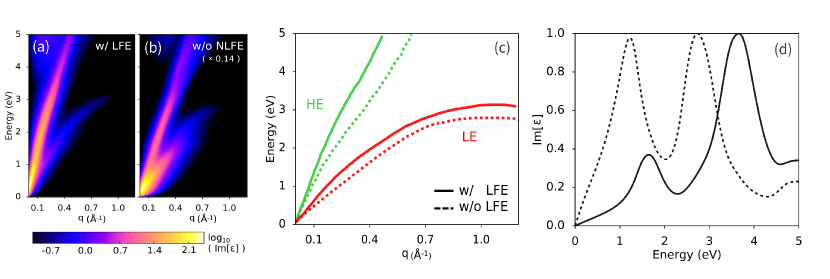
Here, is the XC kernel. The common used XC kernels include adiabatic local density approximation (ALDA) Perdew and Zunger (1981), Bootstrap approximation Sharma et al. (2011), Q-dependent kernals Giuliani and Vignale (2005); Corradini et al. (1998), etc. A simplest case is the so-called random phase approximation (RPA), with . Since the plasmon is demonstrated to be well described in RPA Mar (2006), we use RPA in the following calculation, while some results with other XC kernels such as ALDA are also tested and found to be consistent with RPA results. As indicated in Ref. Cazzaniga et al. (2011), many-body local field effect is not a dominant factor in simple metals such as sodium and aluminum. Thus, although local field effect may be an interesting topic, the Q-dependent kernels are not tested and discussed in this work.
With translational symmetry, it is more convenient to represent in the reciprocal lattice space. Fourier coefficients are written as
| (S5) |
where
| (S6) |
and so is the the Dyson’s equation
| (S7) |
The dielectric function can be expressed with as
| (S8) |
becomes diagonal in reciprocal space
| (S9) |
Note that the kernel is proportional to . This indicates that with increases, the perturbation (the second term in Eq. S7) is decreasing and falling into the valid region of lr-TDDFT.
Thus, the dielectric function is simplified as
| (S10) |
The macroscopic dielectric function is defined by
| (S11) |
We note that, in Eq. S11, the local field effect (LFE) has been included Wiser (1963). Otherwise, the macroscopic dielectric function is
| (S12) |
and describe an inaccurate plasmon dispersion with a small red-shift, as shown in Fig. S2.
For comparison and analysis, simpler approximation called independent particle (IP) is occupied. By setting in Eq. S7,
| (S13) |
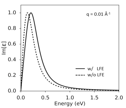
As shown in Fig. S1, the optical response of the borophene, i.e. the long-wavelength plasmon response shows only one major peak at 0.27 eV. As q increases, the single branches split into two branches, as we discussed in the main text.