Efficiency and timing performance of the MuPix7 high-voltage monolithic active pixel sensor
Abstract
The MuPix7 is a prototype high voltage monolithic active pixel sensor with pixels thinned to and incorporating the complete read-out circuitry including a differential data link. Using data taken at the DESY electron test beam, we demonstrate an efficiency of and a time resolution of . The efficiency and time resolution are studied with sub-pixel resolution and reproduced in simulations.
keywords:
Silicon Pixel Detectors , Monolithic Sensors1 Motivation
High-rate precision experiments in particle physics require fast, high-resolution tracking detectors. For low momentum particles, multiple Coulomb scattering in detector material is the main source of tracking uncertainty and thus the material in the tracking volume has to be minimized. High voltage monolithic active pixel sensors (HV-MAPS) [1, 2, 3, 4, 5] allow for the construction of fast, pixelated and thin particle detectors. A commercial high voltage process (AMS HV-CMOS) allows for deep -wells in a -doped substrate; a high voltage of around between the -wells and the substrate creates a thin depletion zone with very large fields, leading to fast charge collection. Inside of the deep -well, shallow and -wells can be placed, allowing for the implementation of CMOS transistors; in particular, an amplifier circuit can be placed directly inside the pixel. As the active region is very thin, most of the substrate can be removed after manufacturing and sensors with a thickness down to only can be obtained.
The Mu3e experiment [6] searches for the lepton-flavour violating decay aiming for a sensitivity of one in decays. In order to track more than electrons and positrons per second and determine their momentum with high precision, four layers of HV-MAPS sensors in a barrel geometry will be used [7]. For accidental background suppression and to ease the reconstruction of tracks in this very high rate environment, a good time resolution of the tracking detector is essential.
In preparation for the Mu3e experiment, we have produced and characterized a series of HV-MAPS prototypes, the MuPix chips [8]. In this series, the MuPix7, is the first prototype incorporating the complete functionality required for the experiment: signals are amplified in the pixel and driven to the chip periphery by a source-follower. A comparator compares the signal to a threshold, which is adjustable individually for each pixel. In case a hit is detected, an eight-bit Gray-encoded timestamp is stored. Priority logic coupled to a state machine collects and serializes the hit times and column and row addresses and sends them off-chip using a low-voltage differential signaling readout link555the chip and link are fully functional up to , we however typically operate it at the lower frequency with 8bit/10bit encoding [9]. The active area of the chip is incorporating a matrix of 32 40 pixels resulting in a pitch of in column direction and in row direction. The sensors were thinned to . A detailed description of the system and global efficiency and noise measurements can be found in reference [10].
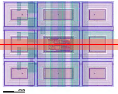
In this work, we present a detailed study of the efficiency and time resolution of the MuPix7 with sub-pixel spatial resolution. This is of particular interest, as there are nine separate, shorted charge-collecting diodes in each pixel, see figure 1, and it has to be ensured that charge is also collected efficiently from the space between the diodes. In fact, charge sharing between pixels is known to be the largest contribution to efficiency losses in MuPix chips. Optimizing the diode geometry to ensure efficient charge collection with the lowest possible capacitance is one of the main goals for further detector development and we thus aim to verify technology computer aided design (TCAD) simulations of our geometry with beam measurements.
The timing resolution in our binary, single threshold readout scheme is mainly driven by variations in signal size (time-walk). In the present study, we try to also identify contributions from charge drift and diffusion as well as signal transmission times.
The homogeneity of the efficiency and timing resolution over the whole chip is of great importance in view of the next step in HV-MAPS development, the production of a large sensor.
2 Measurement set-up
We present results from data taken in March 2016 at the DESY-II beam test facility [11]. Photons are produced via bremsstrahlung by placing carbon fibres in the electron beam of the DESY-II synchrotron; they subsequently convert into electron-positron pairs via pair-production in a metal target. With a dipole magnet, the electrons and positrons are separated and electrons with an energy of were selected with a collimator, resulting in a rate of approximately .
Reference tracks were obtained from the EUDET Telescope Duranta [12], which consists of six planes of monolithic active pixel sensors (MIMOSA 26, [13]). They have a pixel size of and an active area of . The sensors are thick and glued on a protective foil, which sums up to of a radiation length. The maximum track rate that can be read out is . After the first three tracking planes, a device under test (DUT) can be placed on a rotational stage. In this way, a MuPix7 chip was placed as DUT in the center of the telescope. In addition to the pixel sensors, the telescope is equipped with four scintillators – two before, and two after the pixel sensors – read out by photomultiplier tubes (PMTs) used as triggers. A trigger logic unit and the EUDAQ data acquisition framework [14] were used to combine the data streams from the telescope, the scintillators and the DUT. The MuPix7 DUT was operated with a frequency for the timestamps of . We directly fed the scintillator coincidence signal into the field programmable gate array (FPGA) used to read out the MuPix7 sensor, sampling with a clock frequency of , therefore storing the most precise timing information available. The telescope planes were operated with threshold levels corresponding to a collected charge in each individual pixel of at least five times the RMS noise.
A track based alignment of the telescope planes was performed using the Millepede II algorithm with the general broken line track model [15]. This resulted in mean residuals on the telescope planes in a range from to and residual widths below .
3 Efficiency measurement
Straight tracks were fitted through the six telescope planes with an efficiency of () with a DUT rotated by () in the beam. These tracks were then extrapolated to the DUT with an expected position uncertainty on the DUT of () for a DUT rotated by (). Readout events containing a single track of good quality and less than 50 hits on the MuPix7 serve as the reference sample. If a hit within of the extrapolated track intersection with the MuPix7 is found, track and hit are matched. In addition, one noisy pixel on the MuPix7 with a hit rate two orders of magnitude above the average pixel rate was excluded from the analysis.
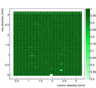
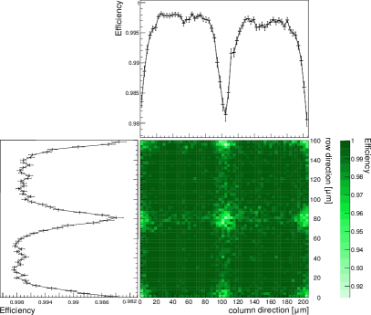
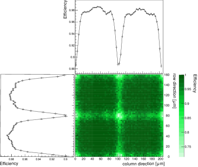
We obtained data samples with two different configurations of the MuPix7: at the optimal working point with high voltage and a threshold of , and at high voltage and a threshold of corresponding to lower efficiency settings. In both cases, a tune of the on-chip bias currents with a power consumption of was applied. For each individual pixel, the local threshold was adjusted to achieve a noise rate below . With the first settings, an average efficiency of was measured (excluding the outer two columns / rows in order to avoid edge effects and the non-connected diodes in the top row), see the efficiency map in figure 2. Inefficiencies are visible mainly in the corners of the pixels, where the charge is shared between four pixels, as can be clearly seen in figure 3, for which all cells of two by two pixels (excluding again the outer two columns / rows) have been stacked on top of each other in order to increase statistics.
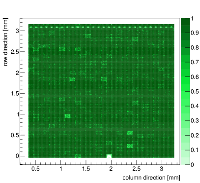
In order to study the charge collection processes affecting the efficiency in more details, we analyzed the data taken with the reduced high voltage, resulting in overall efficiency; see figure 4 for an efficiency map and figure 5 for the stacked two by two pixel cell. As expected, an efficiency drop is primarily observed along the pixel edges, where charge is shared between two pixels. It also becomes evident that hits in the central diode containing the amplifier are more efficiently detected.
4 Timing performance
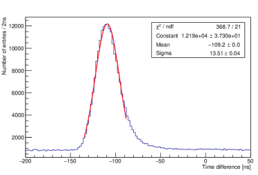
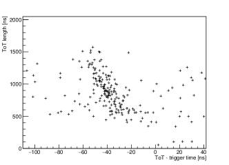
The time resolution was studied by comparing the pixel hit times and the time of the scintillator coincidence, see figure 6. A Gaussian function is fitted to the peak region of the distribution and a core time resolution of (with a negligible contribution from the scintillator setup) is obtained. There is however a sizable tail towards late MuPix hits caused by the time-walk of small signals. For one pixel per MuPix7, the time over threshold information is read out, it is plotted in figure 7 versus the time difference between hits in this pixel and the scintillator coincidence, clearly exhibiting the time-walk behaviour. The hit timestamp in the MuPix7 is saved when the pixel signal crosses the (fixed) comparator threshold. The time resolution can thus be influenced by variations in the signal size due to fluctuations in the collected charge, pixel-to-pixel production variations in the amplifier and comparator circuits, drops of the high, low and bias voltages over the chip as well as the length of signal pathways.
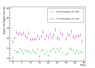
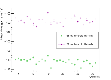
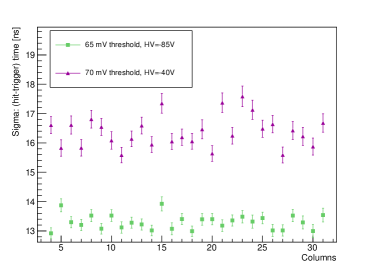
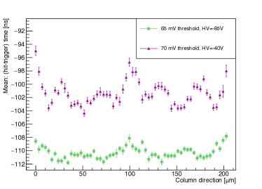
In order to study the spatial variation of the time resolution, we analyzed slices both in column- and row-direction separately. For the spatial distinction, the extrapolated telescope track position of the matched hit was used. For the selected hits, the differences between the hit and all recorded scintillator timestamps of that event were studied using the mean (delay) and width (resolution) obtained from the Gaussian fit.
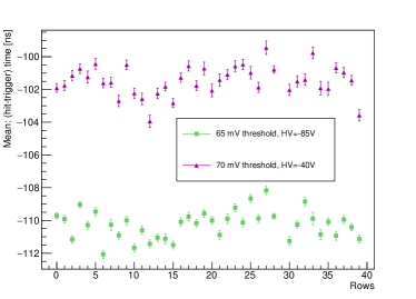
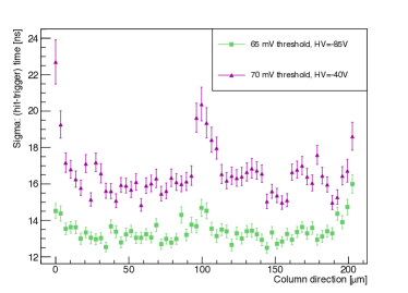
Figures 8 and 9 show the average delay and the resolution of the time measurement in dependence of the row and column axis. In particular the delays vary beyond the purely statistical expectation; however no significant slope is apparent, which indicates that voltage drops over the small chip and signal transmission times do not significantly contribute. Decreasing the high voltage and increasing the threshold leads to later hits with a larger dispersion in time, but also here no structures on the chip are apparent.
In order to study the influence of the signal size on the time measurement, we perform an average over all pixels and study delay and resolution as a function of the hit position in the pixel; towards the edges and corners, charge is shared between several pixels and the signal seen by the pixel under study is thus smaller. This effect is clearly visible in figure 10, where we show the fitted delay and width averaged over two columns using the reduced high voltage/efficiency settings. The signal arrives later and the time resolution is worse at the pixel edge; in addition, effects from the diode structure shown in figure 1 become visible. At , the region between the diodes is not completely depleted and part of the deposited charge is lost due to recombination or collected much slower via diffusion. In addition, the electrical connections between the nine diodes are not ideal conductors; the effective detector capacitance thus becomes a function of the hit position within the pixel.
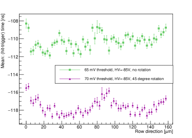
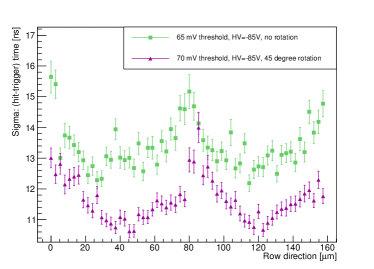
A comparison – using the nominal high voltage and a low threshold – between an unrotated sensor and a sensor rotated horizontally by 45 degrees relative to the incoming particle direction (leading to a signal enhanced by a factor compared to perpendicular operation) is shown in figure 11. The projected pointing resolution in column direction is worsened by the rotation, we thus show the row projections, in which the pixel edges are still visible but significantly reduced and the diode structure is no longer discernible for the rotated sensor. Not surprisingly, a large signal greatly improves the timing performance; in future versions of the MuPix we consequently plan to use a higher resistivity substrate which will lead to a thicker depletion zone and thus a larger collected charge.
5 Simulation
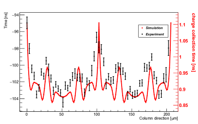
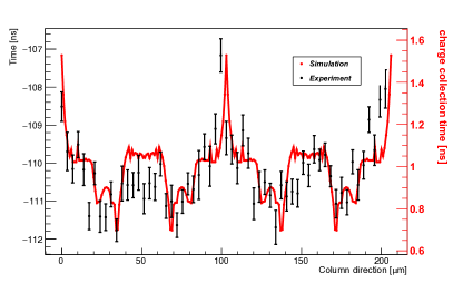
We have simulated the charge collection in the pixel using Synopsys TCAD (Technology Computer Aided Design) tools [16]. The 2-D simulation models a slice through the centre of the pixel in column direction (see figure 1). A linear energy transfer along the particle track of was assumed in the heavy ion model of Sentaurus device [17]. Particle incidence is at a right angle to the sensor and the impact point is varied along the column direction. The charge collection curve in the diode at and is fitted with an exponential and the time constant is determined. The charge collection time is expected to be linearly correlated to the measured latency by an unknown scale factor determined by the amplifier and comparator circuitry. The simulated time constants are plotted in figures 12 and 13 and compared to the measurements, selecting a wide slice in the centre of the pixel (figure 1). Taking into account the limited position resolution of the measurement, all major features are reproduced by the simulation, giving us confidence that simulations can be used to further optimize the charge collection and timing behaviour in future devices.
6 Conclusions
Using the test beam facility at DESY and an EUDET pixel telescope we have performed studies of efficiency and timing resolution of the MuPix7 high voltage monolithic active pixel sensor. At the nominal operation point, the sensor reaches an efficiency of for perpendicular electron tracks. The remaining inefficiency is due to charge sharing between pixels, particularly in the pixel corners; no effect of the segmentation of each individual pixel into nine electrodes is visible.
The time resolution at nominal settings is about ; our study shows that it is dominated by time-walk, which can be easily seen at the pixel edges, where the signal size in the pixel is reduced due to charge sharing between pixels. Measurements with reduced efficiency settings make in-pixel variations due to the split charge collection diode visible and are well modeled by a TCAD simulation. With the larger charge deposited by particles crossing at 45 degrees to the sensor planes, both inefficiencies and sub-pixel timing variations are hardly observable. For future versions of the MuPix, we thus intend to use a higher resistivity substrate, leading to an increased collected charge. We will also explore several schemes for time-walk compensation with the aim of a further reduction of the time resolution.
Acknowledgments
The support of the Deutsches Elektronensynchrotron (DESY, Hamburg), a member of the Helmholtz Association (HGF) providing the test beam and the related infrastructure made this measurement possible. We would especially like to thank the EUDET telescope group at DESY for their valuable support of this test beam measurement.
A. Meneses Gonzales and H. Augustin would like to thank Marta Baselga of the Institut für Experimentelle Teilchenphysik (ETP) des Karlsruher Instituts für Technologie (KIT) for the comprehensive introduction to Synopsys TCAD.
N. Berger, D. vom Bruch, Q. Huang, A. Kozlinskiy and F. Wauters would like to thank the Deutsche Forschungsgemeinschaft for support through an Emmy Noether grant and the PRISMA cluster of excellence at Johannes Gutenberg University Mainz.
M. Kiehn, L. Huth and S. Dittmeier acknowledge support by the International Max Planck Research School for Precision Tests of Fundamental symmetries. H. Augustin and A. Meneses Gonzales acknowledge support by the HighRR research training group (GRK 2058) and A.K. Perrevoort by the Particle Physics beyond the Standard Model research training group (GRK 1940).
References
- [1] I. Peric, A novel monolithic pixelated particle detector implemented in high-voltage CMOS technology, Nucl. Instrum. Meth. A582 (2007) 876–885.
- [2] I. Peric, C. Kreidl, P. Fischer, Particle pixel detectors in high-voltage CMOS technology–New achievements, Nucl. Instrum. Meth. A650 (2010) 158–162.
- [3] I. Peric, C. Takacs, Large monolithic particle pixel-detector in high-voltage CMOS technology, Nucl. Instrum. Meth. A624 (2010) 504 – 508.
- [4] I. Peric, Active pixel sensors in high-voltage CMOS technologies for ATLAS, JINST 7 (2012) C08002.
- [5] I. Peric, et al., High-voltage pixel detectors in commercial CMOS technologies for ATLAS, CLIC and Mu3e experiments, Nucl. Instrum. Meth. A731 (2013) 131–136.
- [6] A. Blondel, et al., Research Proposal for an Experiment to Search for the Decay arXiv:1301.6113.
- [7] N. Berger, et al., A tracker for the Mu3e experiment based on high-voltage monolithic active pixel sensors, Nucl. Instr. Meth. A 732 (2013) 61–65.
- [8] H. Augustin, et al., The MuPix high voltage monolithic active pixel sensor for the Mu3e experiment, JINST 10 (2015) C03044.
- [9] A. X. Widmer, P. A. Franaszek, A DC-Balanced, Partitioned-Block, 8B/10B Transmission Code, IBM Journal of Research and Development 27 (1983) 440.
- [10] H. Augustin, et al., The MuPix System-on-Chip for the Mu3e Experiment, Nucl. Instrum. Meth. A845 (2017) 194.
- [11] T. Behnke, et al., Test Beams at DESY, EUDET-Memo 2007-11.
- [12] H. Jansen, et al., Performance of the EUDET-type beam telescopes, EPJ Techn. Instrum. 3 (2016) 7.
- [13] C. Hu-Guo, et al., First reticule size MAPS with digital output and integrated zero suppression for the EUDET-JRA1 beam telescope, Nucl. Instrum. Meth. A623 (2010) 480–482.
- [14] H. Perrey, EUDAQ and EUTelescope: Software Frameworks for Test Beam Data Acquisition and Analysis, PoS TIPP2014 (2014) 353.
- [15] V. Blobel, C. Kleinwort, F. Meier, Fast alignment of a complex tracking detector using advanced track models, Comput. Phys. Commun. 182 (2011) 1760–1763.
-
[16]
Synopsys Inc., Synopsys
TCAD.
URL https://www.synopsys.com/silicon/tcad.html -
[17]
Synopsys Inc., Sentaurus Device.
URL https://www.synopsys.com/silicon/tcad/device-simulation/sentaurus-device.html