Robustness of the Insulating Bulk in the Topological Kondo Insulator SmB6
Abstract
We used the inverted resistance method to extend the bulk resistivity of SmB6 to a regime where the surface conduction overwhelms the bulk. Remarkably, the bulk resistivity shows an intrinsic thermally activated behavior that changes ten orders of magnitude, suggesting that it is an ideal insulator that is immune to disorder. Non-stoichiometrically-grown SmB6 samples also show an almost identical thermally activated behavior. At low temperatures, however, these samples show a mysterious high bulk resistivity plateau, which may arise from extended defect conduction in a 3D TI.
pacs:
72.10.Bg, 71.10.FkSemiconductors, or narrow band-gapped insulators, have been one of the most important classes of materials both for technological advances in electronics and for fundamental scientific studies in the past several decades. In technology, the realization of the modern electrical and optoelectrical devices that we use today are possible because of the successful control of point defects (donors and acceptors) in semiconductors. In fundamental science studies, semiconductors have provided a fascinating playground for the discovery of new states of matter. One example is 3D topological insulators (TIs)Fu et al. (2007); Moore and Balents (2007), discovered about a decade agoHsieh et al. (2008); Xia et al. (2009); Chen et al. (2009), in which a unique two-dimensional electron gas emerges on the surface due to bulk band inversion. Many of the 3D TIs, however, can easily be found in the degenerate semiconductor regime or even in the hopping conduction regime where they exhibit large bulk conduction due to the presence of unintentional impurities and disorderBrahlek et al. (2015). Obtaining a higher quality bulk in such 3D TIs is an on-going technical challengeBrahlek et al. (2015).
Recently, there has been further excitement about the prediction of 3D TIs in strongly correlated insulatorsDzero et al. (2010); Takimoto (2011). The best candidate is SmB6, a traditionally well-known mixed-valent insulator or Kondo insulator that has a narrow bulk band gapAllen et al. (1979). In the bulk of SmB6, an almost flat 4 band and a dispersive 5 band hybridize at cryogenic temperatures forming a very small band gap at the Fermi level. Theory suggests that this hybridization plays the role of band-inversion, resulting in a 3D TIDzero et al. (2010); Takimoto (2011). Electrical transport experiments unambiguously revealed the existence of the conducting surface at low temperatures (below 3-4 K), consistent with the 3D TI predictionWolgast et al. (2013); Kim et al. (2013). Below 3-4 K, the insulating bulk becomes too resistive for the current to flow in, and the current flows on the conducting surface instead, revealing itself as a resistance plateau. Despite some of the earlier angle-resolved photoemission spectroscopy (ARPES) results suggesting that the conducting surface is from a trivial origin Zhu et al. (2013), most recent experimental works including electricalWolgast et al. (2013); Kim et al. (2013); Wolgast et al. (2015); Nakajima et al. (2016); Syers et al. (2015); Thomas et al. (2016); Wakeham et al. (2015) and thermal transportLuo et al. (2015), de Haas-van Alphen quantum oscillations by angle-dependent magneto-torque magnetometryLi et al. (2014), ARPESNeupane et al. (2013); Denlinger et al. (2014); Jiang et al. (2013); Xu et al. (2014a, 2013), scanning tunneling microscopyYee et al. (2013); Rößler et al. (2014); Miyamachi et al. , point contact spectroscopyZhang et al. (2013), planar tunneling spectroscopyPark et al. (2016); Sun et al. (2017), and neutron scatteringFuhrman et al. (2015) have provided strong evidence of the existence of conducting surface states that is consistent with the unique properties of a 3D TI. There are even reports of the helical spin-structure, which is one of the most unique properties of a topologically protected surface, by spin-resolved ARPES measurementsXu et al. (2014b) and a recent report of a spin-signal on the surface by the inverse Edelstein effectSong et al. (2016).
The quantum oscillations by magneto-torque measurements have provided the research community with some of the most exciting yet confusing results in this material system. G. Li .Li et al. (2014) report on quantum oscillations indicating the presence of 2D Fermi pockets on the (100) and (110) surfaces. Furthermore, the extrapolation of the Landau indices from the oscillations to the infinite magnetic field limit reveals a Berry phase contribution that is consistent with the Dirac-like dispersion that emerges in a 3D TI. In contrast, B. S. Tan . Tan et al. (2015) later report on quantum oscillations with a non-2D angle dependence, deviation of the standard Lifshitz-Kosevich temperature dependence, a Berry phase that is non-Dirac-like, and oscillation amplitudes that do not depend on the surface facets. They conclude that their oscillations originate from an unconventional Fermi surface in the insulating bulk. The possibility of having a material with a bulk Fermi surface in the absence of a conducting Fermi liquid resulted in further excitement about SmB6. To explain the unconventional Fermi surface of the bulk, new theories have been developed involving exotic excitations that couple to the magnetic field but not the electric fieldErten et al. (2017); Knolle and Cooper (2017).
Vibrant research in the past several years has been motivated by both the need of verifying the 3D TI properties and the search for new exotic bulk phenomena of SmB6. One aspect, however, that remains yet elusive is the role of disorder. For example, some of the early studies of SmB6 report that samples with vacancies result in a lower resistance plateauKasuya et al. (1977) that is inconsistent with the 3D TI picture. This is inconsistent because higher vacancy levels are expected to introduce higher disorder on the surface, and therefore they should have higher surface resistivity. Also to the best of our knowledge, many recent experimental conclusions and theoretical predictions, including the interpretations of the quantum oscillation reports, assume that the SmB6 crystal is close to ideal. We believe it is critically important to consider the role of disorder in the bulk in more depth before the community moves on to discuss new exciting intrinsic properties of the SmB6 crystals.
In this letter, we use transport measurements on SmB6, including stoichiometrically- and non-stoichiometrically-grown samples, to study the role of disorder in the bulk. We first note that the characterization of bulk transport in the presence of significant surface conduction is challenging. We have previously argued that the common practice of presenting the residual-resistance ratio from conventional four-contact resistance measurements is limited when interpreting a material system that has both surface and bulk conducting statesEo et al. (2017). In this study, we use the inverted resistance measurement technique, which was proposed by the authors recentlyEo et al. (2017). Inverted resistance measurements performed on multi-ring Corbino structures allows us to properly characterize the bulk conduction even in the presence of strong surface conduction. We demonstrate the substantial difference when we choose a typical four-contact measurement compared to a proper Corbino disk measurement in Supplementary A.
| Sample | (meV) | (k) | Hardness(kp) | |
|---|---|---|---|---|
| S1 | 0 | 4.01 | 3.1 | 2191 125 |
| S2 | 0.1 | 4.12 | 1.6 | 1913 16.5 |
| S3 | 0.25 | 3.97 | 1.5 | 1781 111 |
| S4 | 0.40 | 3.85 | 2.8 | 1563 50.8 |
Single crystalline samples were grown by the Al-flux technique. The mixture of Samarium pieces (Ames Lab, 99.99 ), Boron powder (99.99 ) and Aluminum shots (99.999 ) was placed in an alumina crucible and loaded in a vertical tube furnace with ultra high-purity Ar flow. We grew samples with different starting compositions of Sm: B: Al = 1-: 6: 700, where is the starting composition ratio, ranging from 0 to 0.40. We expect sample S1 in which =0 to be stoichiometric, whereas the other samples are expected to have a higher disorder level. X-ray and Auger electron spectroscopy measurements did not have the resolution to unambiguously determine the point defect levels, but we do see differences that indicate the overall physical properties are changing from hardness measurements. A detailed description is presented in Supplementary B.
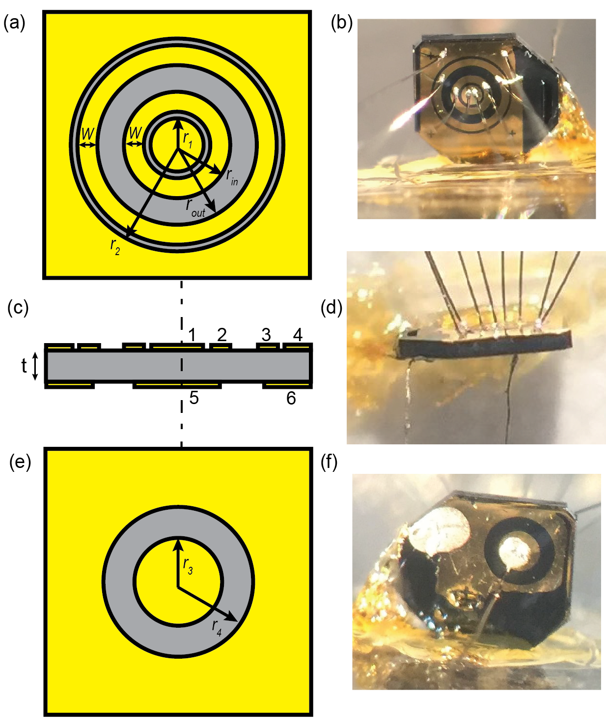
To illustrate the inverted resistance method in short, the transport geometry is shown in Fig. 1. The samples were fine polished with a final step of aluminum oxide slurry that has a particle size of 0.3 m. The Corbino-disk patterns were fabricated using standard photolithography, followed by ebeam evaporation of Ti/Au (20Å/1500Å). We used a home-built instrumentation amplifier in addition to an external lock-in amplifier in the Dynacool PPMS for measurement. A four-terminal Corbino disk can be measured by (= /), which can be regarded as a standard resistance measurement (). In the surface dominated regime, below 3-4 K, the inverted resistance () can be measured by either or . If the change in surface resistivity with temperature is not strong compared to the bulk, the standard two-channel model is a good approximation that works well for in the full temperature range:
| (1) |
where the geometric prefactor is ln for a Corbino disk, and is the effective thickness that asympotically approaches when the sample is very thin, but is independent of when the sample is very thickEo et al. (2017). The inverted resistance below the bulk-to-surface crossover temperature follows:
| (2) |
where is a prefactor for the inverted resistance. The corresponding and are found from finite element analysis, similar to the derivation of bulk resistivity extraction in Ref. Eo et al. (2017). The detailed method is presented in Supplementary C.
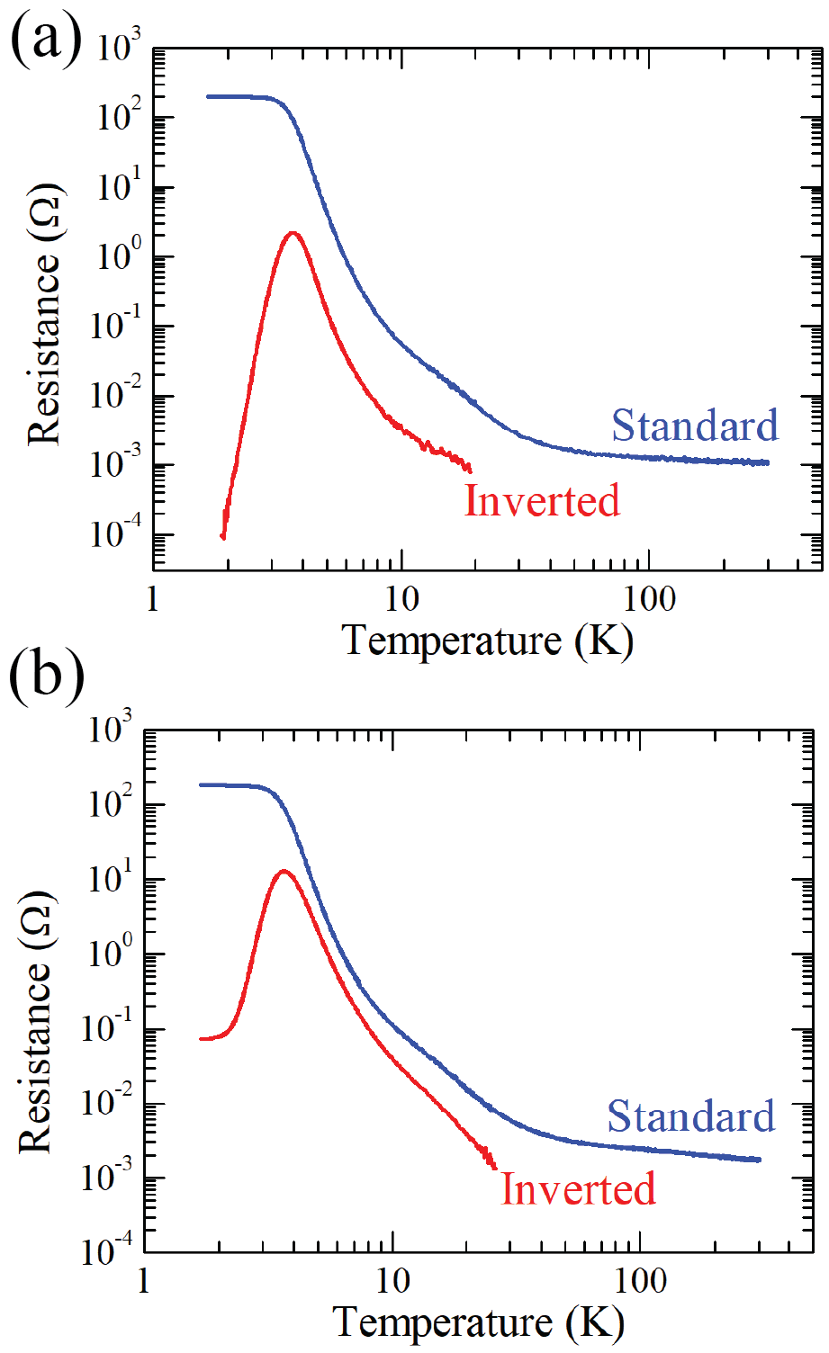
Fig. 2 (a) shows the measured resistance ( (blue) and (red)) from sample S1. The qualitative behavior of Fig. 2 (a) is consistent with what we expect when the bulk resistivity is governed intrinsically, , where is the activation energy. In the high-temperature regime, above 4 K, both and increase when the temperature is lowered, consistent with Eq. 1 in the bulk-dominated regime (). Below 4 K, develops a plateau which corresponds to a sheet resistance of = 3 k according to Eq. 1 in the surface-dominated regime (). , on the other hand, drops as the temperature is lowered. This is consistent with Eq. 2 when the bulk resistivity follows . Below 1.99 K, the inverted resistance becomes too small, and the measurement is limited by the amplifier performance. Here, we only present the data that is meaningful, above this performance limit.
Next, we consider the non-stoichiometrically-grown SmB6 samples. We present the sample S4 results in Fig. 2 (b). In the bulk-dominated regime, above 4 K, the temperature response of the resistances of all samples behaved qualitatively identically to sample S1 results. In the surface-dominated regime, below 4 K, shows a plateau that corresponds to a in the 1 - 3 k range. In contrast, in the surface-dominated regime drops at first, consistent with Eq. 2 when the bulk resistivity is keeps rising. Below 2.5 K, however, the resistance becomes much weakly dependent of temperature. The magnitude of this resistance plateau becomes lower for samples that are grown with less Sm.
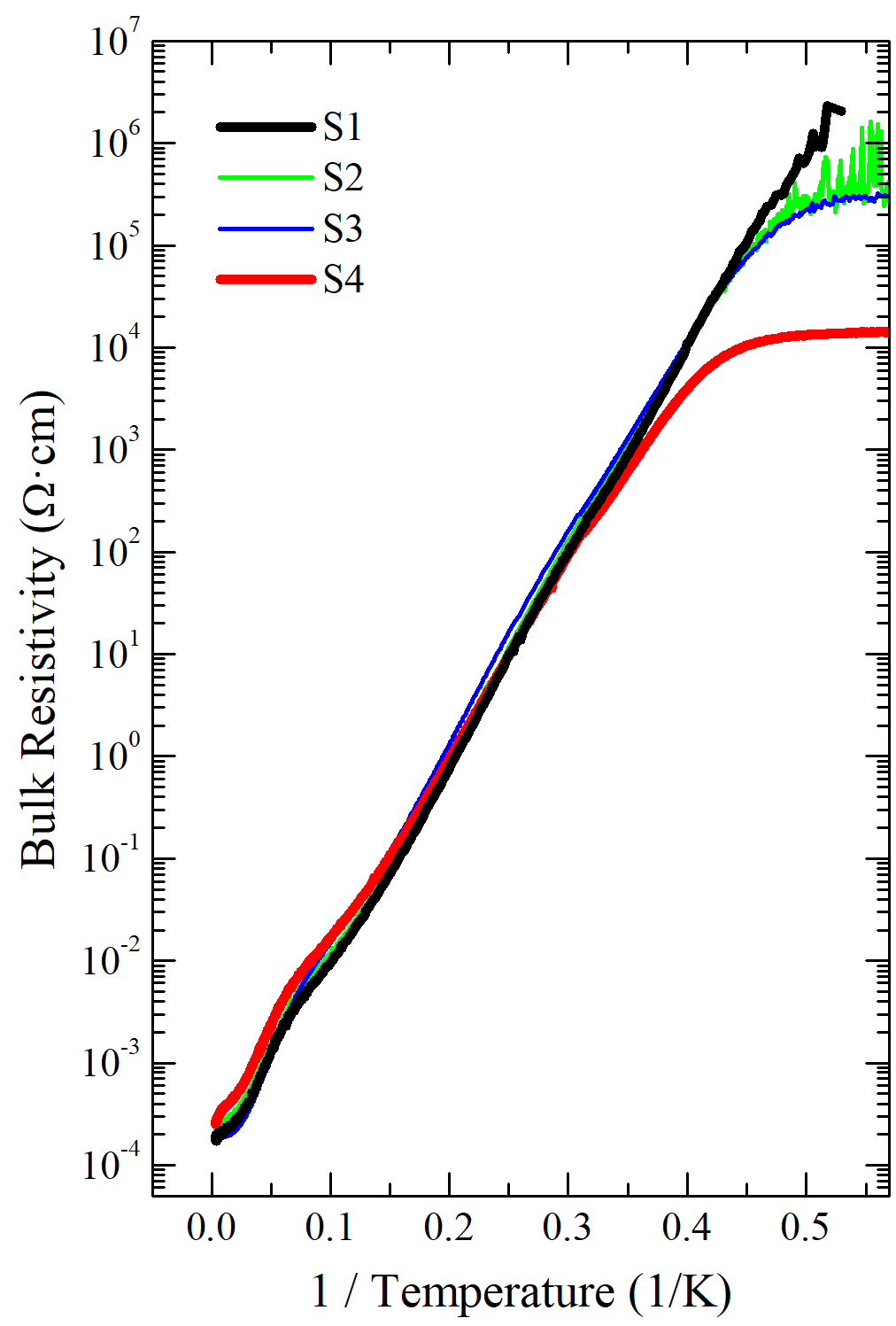
The bulk resistivities converted from the resistance measurements are shown in Fig. 3. Sample S1 (shown in black) shows a thermally activated exponential behavior (Ea = 4.01 meV) with a change of 10 orders of magnitude. The resistivity shows an intrinsic semiconductor behavior in the full temperature range, without showing any signs of the extrinsic regime of a semiconductor. Below 0.4 K-1 (or above 2.5 K), the non-stoichiometrically-grown SmB6 samples (Samples S2, S3, and S4) show almost identical activation energies, and the resistivity rises at least 7 orders of magnitude.
It is well known from previous Hall measurements that the bulk resistivity rise of SmB6 is due to the thermally activated bulk carriers, and the mobility changes within two orders of magnitude (Allen et al., 1979; Molnar et al., 1982; Kasuya et al., 1983; Sluchanko et al., 1999, 2000). In our stoichiometrically-grown sample (sample S1) result , the activation behavior continues at low temperatures indicating a decrease in carrier density of 10 orders of magnitude. We, therefore, estimate a carrier density of (1/cm3) at 1.99 K. This implies that there are only carriers in the bulk region of our sample at this temperature, and there would be less than 1 bulk carrier below 1 K by extrapolating the thermally activated behavior. The non-stoichiometrically-grown samples (Samples S2, S3, and S4) also indicate that no more than (1/cm3) bulk carriers are left before the bulk resistivity saturates below 2.5 K. For the saturation of the non-stoichiometrically-grown samples, the magnitudes are too high for them to be attributed to the extrinsic regime of a non-degenerate semiconductor when there are point defects. Note that the associated number of carriers of these resisitivity plateaus, of course, is too small to explain the exotic bulk quantum oscillations seen by Tan Tan et al. (2015). Also, none of the data resembles close to the temperature dependence of the Mott-type variable range hopping conduction (). Recent AC conductivity measurements show large conduction that completely ruling out the impurity conduction scenario in the bulk is worrisomeLaurita et al. (2016, 2017). However, the conduction does not appear in the DC limit, consistent with our results. Our data show strong evidence that the bulk gap of SmB6 does not involve point defect-like impurity states that can contribute to DC transport, and therefore the bulk is robust. It is important to note that this is in stark contrast to other hexaboride systems such as CaB6Stankiewicz et al. (2016); Rhyee and Cho (2004); Vonlanthen et al. (2000), SrB6Stankiewicz et al. (2016); Ott et al. (1997), BaB6Stankiewicz et al. (2016), YbB6Kim et al. (2007); Tarascon et al. (1980), and EuB6Wigger et al. (2004); Kasuya et al. (1980), which all show strong dependence of disorder in the temperature-dependent resistivity measurements. This result is also promising when comparing to the bulk of other 3D TIs, where purifying bulk is an ongoing challengeAndo (2013); Brahlek et al. (2015).
To the best of our knowledge, the robust intrinsic insulating behavior and the high bulk resistivity plateau in the non-stoichiometrically-grown samples cannot be explained by standard theory of disorder. We have previously reported that the picture of shallow impurity states, or in-gap states, in SmB6 are not justified by the effective mass approximation framework because the effective Bohr radius, , is comparable or smaller than the lattice constantRakoski et al. (2017). The small resisitivity feature around 14 K can be explained by the alternative model with a clean gap and band banding by the surface statesRakoski et al. (2017). We find the most similar case, where the bulk gap appears to be uninterrupted by point defects, is the BCS gap in superconductors. It is well known that the BCS gap withstands dirty conditions, as long as the impurity is non-magneticAnderson (1959).
Within the framework that the bulk gap is robust against point defects, to understand the mysterious high bulk resistivity plateaus in the non-stoichiometrically-grown samples, it is most reasonable to think that the conduction path has a confined or lower-dimensional current channel instead of a homogeneous channel in the bulk. One plausible theory is that extended defects, such as grain boundaries and threading dislocations, conduct because SmB6 can harbor topologically protected edge conduction. Particularly, the possibility of 1D dislocation conduction in a 3D TI is a further excitement, as it is a unique 1D edge conduction channel that is not localized by disorderRan et al. (2009). These need not be uniformly distributed, but instead exist sporadically with length scales that extend throughout the bulk of the sample. The cause of these high-order defects may be related to the inhomogeneity in the bulk. Our hardness and X-ray measurements, which are presented in the Supplementary B, show that all sample indeed have different physical properties, and signatures of disorder present in the crystal. In particular, in the single crystal X-ray diffraction measurement, we observe signatures of twinning in some of our samples. Lastly, it is worth to note that recent SmB6 studies focus on the role of impurities. Heat capacity on vacancy and impurity doped SmB6 show a virtual metallic-like behavior at low temperatures from the bulkValentine et al. (2017); Fuhrman et al. (2017), and recent thermal transport measurements show field-dependent thermal conductivity enhancement depending on the sample qualityBoulanger et al. (2017). We do not yet find a clear connection between these results and our bulk transport plateaus at low temperatures. For future studies, this mysterious bulk conduction channel must be studied in more depth, which include ongoing studies of other variously doped SmB6 samples.
In conclusion, the bulk transport of stoichiometrically- and non-stoichiometrically-grown SmB6 samples were studied through the inverted resistance measurement. Using the double-sided Corbino disk geometry, the stoichiometrically-grown SmB6 sample shows a robust thermally activated bulk resistivity rise. In the non-stoichiometrically-grown SmB6 samples, grown with substantially less samarium, these samples show an almost identical thermally activated behavior until an unexpected resistivity plateau develops. Our results suggest that the bulk of SmB6 is immune to disorder originating from point defects, but may be influenced by extended defects. We believe the robust insulating bulk in SmB6 is important for TI applications. For example, in spintronics applications, there would be no parallel channel from the bulk. For topological quantum computers, because the lifetime of the Majorana modes will not be limited by the bulk channel, we expect the Majorana modes to be well defined.
Acknowledgements.
We thank J. W. Allen, K. Sun, and J. Denlinger for useful discussions and advice on improving the manuscript. We also thank B. L. Scott for the discussion of the single crystal X-ray diffraction data, and Zhongrui(Jerry) Li for assistance with the Auger electron spectroscopy experiments. Funding for this work was provided by NSF Grants No. DMR1441965 and No. DMR-1643145. P. F. S. R acknowledges support from the Laboratory Directed Research and Development program of Los Alamos National Laboratory under project number 20160085DR.References
- Fu et al. (2007) L. Fu, C. L. Kane, and E. J. Mele, Phys. Rev. Lett. 98, 106803 (2007).
- Moore and Balents (2007) J. E. Moore and L. Balents, Phys. Rev. B 75, 121306 (2007).
- Hsieh et al. (2008) D. Hsieh, D. Qian, L. Wray, Y. Xia, Y. Hor, R. Cava, and M. Hasan, Nature 452, 970 (2008).
- Xia et al. (2009) Y. Xia, D. Qian, D. Hsieh, L. Wray, A. Pal, H. Lin, A. Bansil, D. Grauer, Y. Hor, R. Cava, et al., Nat. Phys. 5, 398 (2009).
- Chen et al. (2009) Y. Chen, J. Analytis, J.-H. Chu, Z. Liu, S.-K. Mo, X.-L. Qi, H. Zhang, D. Lu, X. Dai, Z. Fang, et al., Science 325, 178 (2009).
- Brahlek et al. (2015) M. Brahlek, N. Koirala, N. Bansal, and S. Oh, Solid State Commun. 215-216, 54 (2015).
- Dzero et al. (2010) M. Dzero, K. Sun, V. Galitski, and P. Coleman, Phys. Rev. Lett. 104, 106408 (2010).
- Takimoto (2011) T. Takimoto, J. Phys. Soc. Jpn. 80, 123710 (2011).
- Allen et al. (1979) J. W. Allen, B. Batlogg, and P. Wachter, Phys. Rev. B 20, 4807 (1979).
- Wolgast et al. (2013) S. Wolgast, C. Kurdak, K. Sun, J. W. Allen, D.-J. Kim, and Z. Fisk, Phys. Rev. B 88, 180405 (2013).
- Kim et al. (2013) D. Kim, S. Thomas, T. Grant, J. Botimer, Z. Fisk, and J. Xia, Sci. Rep. 3, 3150 (2013).
- Zhu et al. (2013) Z.-H. Zhu, A. Nicolaou, G. Levy, N. Butch, P. Syers, X. Wang, J. Paglione, G. Sawatzky, I. Elfimov, and A. Damascelli, Phys. Rev. Lett. 111, 216402 (2013).
- Wolgast et al. (2015) S. Wolgast, Y. S. Eo, T. Öztürk, G. Li, Z. Xiang, C. Tinsman, T. Asaba, B. Lawson, F. Yu, J. W. Allen, et al., Phys. Rev. B 92, 115110 (2015).
- Nakajima et al. (2016) Y. Nakajima, P. Syers, X. Wang, R. Wang, and J. Paglione, Nat. Phys. 12, 213 (2016).
- Syers et al. (2015) P. Syers, D. Kim, M. S. Fuhrer, and J. Paglione, Phys. Rev. Lett. 114, 096601 (2015).
- Thomas et al. (2016) S. Thomas, D. Kim, S. Chung, T. Grant, Z. Fisk, and J. Xia, Phys. Rev. B 94, 205114 (2016).
- Wakeham et al. (2015) N. Wakeham, Y. Q. Wang, Z. Fisk, F. Ronning, and J. D. Thompson, Phys. Rev. B 91, 085107 (2015).
- Luo et al. (2015) Y. Luo, H. Chen, J. Dai, Z.-a. Xu, and J. D. Thompson, Phys. Rev. B 91, 075130 (2015).
- Li et al. (2014) G. Li, Z. Xiang, F. Yu, T. Asaba, B. Lawson, P. Cai, C. Tinsman, A. Berkley, S. Wolgast, Y. S. Eo, et al., Science 346, 1208 (2014).
- Neupane et al. (2013) M. Neupane, N. Alidoust, S. Xu, T. Kondo, Y. Ishida, D.-J. Kim, C. Liu, I. Belopolski, Y. Jo, T.-R. Chang, et al., Nat. Commun. 4, 2991 (2013).
- Denlinger et al. (2014) J. D. Denlinger, J. W. Allen, J.-S. Kang, K. Sun, B.-I. Min, D.-J. Kim, and Z. Fisk, in JPS Conf. Proc. 3 (2014) p. 017038.
- Jiang et al. (2013) J. Jiang, S. Li, T. Zhang, Z. Sun, F. Chen, Z. Ye, M. Xu, Q. Ge, S. Tan, X. Niu, et al., Nat. Commun. 4, 3010 (2013).
- Xu et al. (2014a) N. Xu, C. Matt, E. Pomjakushina, X. Shi, R. Dhaka, N. Plumb, M. Radović, P. Biswas, D. Evtushinsky, V. Zabolotnyy, et al., Phys. Rev. B 90, 085148 (2014a).
- Xu et al. (2013) N. Xu, X. Shi, P. K. Biswas, C. E. Matt, R. S. Dhaka, Y. Huang, N. C. Plumb, M. Radović, J. H. Dil, E. Pomjakushina, K. Conder, A. Amato, Z. Salman, D. M. Paul, J. Mesot, H. Ding, and M. Shi, Phys. Rev. B 88, 121102 (2013).
- Yee et al. (2013) M. M. Yee, Y. He, A. Soumyanarayanan, D.-J. Kim, Z. Fisk, and J. E. Hoffman, arXiv:1308.1085 (2013).
- Rößler et al. (2014) S. Rößler, T.-H. Jang, D.-J. Kim, L. Tjeng, Z. Fisk, F. Steglich, and S. Wirth, Proc. Natl. Acad. Sci. U.S.A 111, 4798 (2014).
- (27) T. Miyamachi, S. Suga, M. Ellguth, C. Tusche, C. M. Schneider, F. Iga, and F. Komori, Sci. Rep. 7, 12837.
- Zhang et al. (2013) X. Zhang, N. Butch, P. Syers, S. Ziemak, R. L. Greene, and J. Paglione, Phys. Rev. X 3, 011011 (2013).
- Park et al. (2016) W. K. Park, L. Sun, A. Noddings, D.-J. Kim, Z. Fisk, and L. H. Greene, Proc. Natl. Acad. Sci. U.S.A. 113, 6599 (2016).
- Sun et al. (2017) L. Sun, D.-J. Kim, Z. Fisk, and W. Park, Phys. Rev. B 95, 195129 (2017).
- Fuhrman et al. (2015) W. Fuhrman, J. Leiner, P. Nikolić, G. E. Granroth, M. B. Stone, M. D. Lumsden, L. DeBeer-Schmitt, P. A. Alekseev, J.-M. Mignot, S. Koohpayeh, et al., Phys. Rev. Lett. 114, 036401 (2015).
- Xu et al. (2014b) N. Xu, P. Biswas, R. Dhaka, G. Landolt, S. Muff, C. Matt, X. Shi, N. Plumb, M. Radovic, E. Pomjakushina, et al., Nat. Commun. 5, 4566 (2014b).
- Song et al. (2016) Q. Song, J. Mi, D. Zhao, T. Su, W. Yuan, W. Xing, Y. Chen, T. Wang, T. Wu, X. H. Chen, et al., Nat. Commun. 7 (2016).
- Tan et al. (2015) B. Tan, Y.-T. Hsu, B. Zeng, M. C. Hatnean, N. Harrison, Z. Zhu, M. Hartstein, M. Kiourlappou, A. Srivastava, M. Johannes, et al., Science 349, 287 (2015).
- Erten et al. (2017) O. Erten, P.-Y. Chang, P. Coleman, and A. M. Tsvelik, Phys. Rev. Lett. 119, 057603 (2017).
- Knolle and Cooper (2017) J. Knolle and N. R. Cooper, Phys. Rev. Lett. 118, 096604 (2017).
- Kasuya et al. (1977) T. Kasuya, K. Kojima, and M. Kasaya, in Valence Instabilities and Related Narrow-Band Phenomena (Springer, 1977) pp. 137–152.
- Eo et al. (2017) Y. Eo, K. Sun, Ç. Kurdak, D.-J. Kim, and Z. Fisk, arXiv:1708.05762 (2017).
- Molnar et al. (1982) S. v. Molnar, T. Theis, A. Benoit, A. Briggs, J. Flouquet, J. Ravex, and Z. Fisk, in Valence instabilities (1982).
- Kasuya et al. (1983) T. Kasuya, M. Kasaya, K. Takegahara, T. Fujita, T. Goto, A. Tamaki, M. Takigawa, and H. Yasuoka, J. Magn. Magn. Mater 31, 447 (1983).
- Sluchanko et al. (1999) N. Sluchanko, A. Volkov, V. Glushkov, B. Gorshunov, S. Demishev, M. Kondrin, A. Pronin, N. Samarin, Y. Bruynseraede, V. Moshchalkov, et al., J. Exp. Theor. Phys 88, 533 (1999).
- Sluchanko et al. (2000) N. E. Sluchanko, V. V. Ġlushkov, B. P. Gorshunov, S. V. Demishev, M. V. Kondrin, A. A. Pronin, A. A. Volkov, A. K. Savchenko, G. Grüner, Y. Bruynseraede, V. V. Moshchalkov, and S. Kunii, Phys. Rev. B 61, 9906 (2000).
- Laurita et al. (2016) N. J. Laurita, C. M. Morris, S. M. Koohpayeh, P. F. S. Rosa, W. A. Phelan, Z. Fisk, T. M. McQueen, and N. P. Armitage, Phys. Rev. B 94, 165154 (2016).
- Laurita et al. (2017) N. Laurita, C. Morris, S. Koohpayeh, W. Phelan, T. McQueen, and N. Armitage, Physica B Condens Matter (2017).
- Stankiewicz et al. (2016) J. Stankiewicz, P. F. Rosa, P. Schlottmann, and Z. Fisk, Phys. Rev. B 94, 125141 (2016).
- Rhyee and Cho (2004) J.-S. Rhyee and B.-K. Cho, J. Appl. Phys 95, 6675 (2004).
- Vonlanthen et al. (2000) P. Vonlanthen, E. Felder, L. Degiorgi, H. R. Ott, D. P. Young, A. D. Bianchi, and Z. Fisk, Phys. Rev. B 62, 10076 (2000).
- Ott et al. (1997) H. Ott, M. Chernikov, E. Felder, L. Degiorgi, E. Moshopoulou, J. Sarrao, and Z. Fisk, Zeitschrift für Physik B Condensed Matter 102, 337 (1997).
- Kim et al. (2007) J. Kim, N. Sung, and B. Cho, J. Appl. Phys. 101, 09D512 (2007).
- Tarascon et al. (1980) J.-M. Tarascon, J. Etourneau, P. Dordor, P. Hagenmuller, M. Kasaya, and J. Coey, J. Appl. Phys 51, 574 (1980).
- Wigger et al. (2004) G. Wigger, R. Monnier, H. Ott, D. Young, and Z. Fisk, Phys. Rev. B 69, 125118 (2004).
- Kasuya et al. (1980) T. Kasuya, K. Takegahara, M. Kasaya, Y. Isikawa, and T. Fujita, Le Journal de Physique Colloques 41, C5 (1980).
- Ando (2013) Y. Ando, J. Phys. Soc. Jpn 82, 102001 (2013).
- Rakoski et al. (2017) A. Rakoski, Y. S. Eo, K. Sun, and i. m. c. Kurdak, Phys. Rev. B 95, 195133 (2017).
- Anderson (1959) P. W. Anderson, J. Phys. Chem. Solids 11 (1959).
- Ran et al. (2009) Y. Ran, Y. Zhang, and A. Vishwanath, Nat. Phys. 5 (2009).
- Valentine et al. (2017) M. E. Valentine, S. Koohpayeh, W. A. Phelan, T. M. McQueen, P. F. Rosa, Z. Fisk, and N. Drichko, Physica B Condens Matter (2017).
- Fuhrman et al. (2017) W. T. Fuhrman, J. R. Chamorro, P. A. Alekseev, J.-M. Mignot, T. Keller, P. Nikolic, T. M. McQueen, and C. L. Broholm, arXiv:1707.03834 (2017).
- Boulanger et al. (2017) M. Boulanger, F. Laliberté, S. Badoux, N. Doiron-Leyraud, W. Phelan, S. Koohpayeh, T. McQueen, X. Wang, Y. Nakajima, T. Metz, et al., arXiv:1709.10456 (2017).