Production and Integration of the ATLAS Insertable B-Layer \AtlasAbstract During the shutdown of the CERN Large Hadron Collider in 2013-2014, an additional pixel layer was installed between the existing Pixel detector of the ATLAS experiment and a new, smaller radius beam pipe. The motivation for this new pixel layer, the Insertable B-Layer (IBL), was to maintain or improve the robustness and performance of the ATLAS tracking system, given the higher instantaneous and integrated luminosities realised following the shutdown. Because of the extreme radiation and collision rate environment, several new radiation-tolerant sensor and electronic technologies were utilised for this layer. This paper reports on the IBL construction and integration prior to its operation in the ATLAS detector. \AtlasDate \AtlasDOI10.1088/1748-0221/13/05/T05008
The ATLAS IBL Collaboration
B. Abbott33, J. Albert47, F. Alberti28a, M. Alex13, G. Alimonti28a, S. Alkire11, P. Allport23,101, S. Altenheiner13, L.S. Ancu7,14, E. Anderssen4, A. Andreani28a,28b, A. Andreazza28a,28b, B. Axen4, J. Arguin4,102, M. Backhaus9,112, G. Balbi8a, J. Ballansat1, M. Barbero9,27, G. Barbier14, A. Bassalat35,103, R. Bates16, P. Baudin1, M. Battaglia38, T. Beau25, R. Beccherle15a,104, A. Bell53, M. Benoit35, A. Bermgan11, C. Bertsche33, D. Bertsche33, J. Bilbao de Mendizabal14,105, F. Bindi8a,17, M. Bomben25, M. Borri26, C. Bortolin10, N. Bousson27, R.G. Boyd33, P. Breugnon27, G. Bruni8a, J. Brossamer4, M. Bruschi8a, P. Buchholz40, E. Budun10, C. Buttar16, F. Cadoux14, G. Calderini25, L. Caminada4,107, M. Capeans10, R. Carney4, G. Casse23, A. Catinaccio10, M. Cavalli-Sforza2, M. Červ10, A. Cervelli7,8a, C.C. Chau44,106, J. Chauveau25, S.P. Chen39, M. Chu43, M. Ciapetti10, V. Cindro24, M. Citterio28a, A. Clark14, M. Cobal46a,46b, S. Coelli28a, J. Collot18, O. Crespo-Lopez10, G.F. Dalla Betta45, C. Daly39, G. D’Amen8a,8b, N. Dann26, V. Dao52, G. Darbo15a, C. DaVia26, P. David1, S. Debieux14, P. Delebecque1, F. De Lorenzi21, R. de Oliveira10, K. Dette10,13, W. Dietsche9, B. Di Girolamo10, N. Dinu35, F. Dittus10, D. Diyakov10, F. Djama27, D. Dobos10, P. Dondero15a,15b,108, K. Doonan16, J. Dopke10,48, O. Dorholt36, S. Dube4,109, D. Dzahini18, K. Egorov10, O. Ehrmann6, K. Einsweiler4, S. Elles1, M. Elsing10, L. Eraud18, A. Ereditato7, A. Eyring9, D. Falchieri8a,8b, A. Falou35, C. Fausten48, A. Favareto15a,15b, Y. Favre14, S. Feigl10, S. Fernandez Perez10, D. Ferrere14, J. Fleury4,110, T. Flick48, D. Forshaw23, D. Fougeron27, L. Franconi36 A. Gabrielli8a,8b,4, R. Gaglione1, C. Gallrapp10, K.K. Gan32, M. Garcia-Sciveres4, G. Gariano15a, T. Gastaldi27, I. Gavrilenko50, A. Gaudiello15a,15b, N. Geffroy1, C. Gemme15a, F. Gensolen27, M. George17, P. Ghislain25, N. Giangiacomi8a,8b, S. Gibson10,111, M.P. Giordani46a,46b, D. Giugni10,28a, H. Gjersdal36, K.W. Glitza48,∗, D. Gnani4, J. Godlewski10, L. Gonella9,101, S. Gonzalez-Sevilla14, I. Gorelov30, A. Gorišek24, C. Gössling13, S. Grancagnolo5, H. Gray10,4, I. Gregor12, P. Grenier41, S. Grinstein2, A. Gris10, V. Gromov31, D. Grondin18, J. Grosse-Knetter17, F. Guescini14,113, E. Guido15a,15b,114, P. Gutierrez33 G. Hallewell27, N. Hartman4, S. Hauck39, J. Hasi41, A. Hasib33, F. Hegner12, S. Heidbrink40, T. Heim10,48,4, B. Heinemann4,12, T. Hemperek9, N.P. Hessey31,113, M. Hetmánek37, R.R. Hinman4, M. Hoeferkamp30, T. Holmes4, J. Hostachy18, S.C. Hsu39, F. Hügging9, C. Husi14, G. Iacobucci14, I. Ibragimov40, J. Idarraga35, Y. Ikegami22, T. Ince29, R. Ishmukhametov32, J. M. Izen49, Z. Janoška37, J. Janssen9, L. Jansen31, L. Jeanty4, F. Jensen4,115, J. Jentzsch10,13, S. Jezequel1, J. Joseph4, H. Kagan32, M. Kagan41, M. Karagounis9,116, R. Kass32, A. Kastanas3, C. Kenney41, S. Kersten48, P. Kind48, M. Klein11, R. Klingenberg13,∗, R. Kluit31, M. Kocian41, E. Koffeman31, O. Korchak37, I. Korolkov2, I. Kostyukhina-Visoven27, S. Kovalenko48, M. Kretz19, N. Krieger17, H. Krüger9, A. Kruth9,117, A. Kugel19, W. Kuykendall39, A. La Rosa14,29, C. Lai 26, K. Lantzsch10, C. Lapoire9,10, D. Laporte25, T. Lari28a, S. Latorre28a, M. Leyton49,2, B. Lindquist42, K. Looper32, I. Lopez2, A. Lounis35, Y. Lu4,118, H.J. Lubatti39, S. Maeland3, A. Maier29,10, U. Mallik20, F. Manca28a, B. Mandelli10, I. Mandić24, D. Marchand18, G. Marchiori25, M. Marx39, N. Massol1, P. Mättig48, J. Mayer39, G. Mc Goldrick44, A. Mekkaoui4, M. Menouni27, J. Menu18, C. Meroni28a, J. Mesa14, S. Michal10,14, S. Miglioranzi10,46a,46b, M. Mikuž24, A. Miucci14,7, K. Mochizuki27,102, M. Monti 28a, J. Moore32, P. Morettini15a, A. Morley10,51, J. Moss32, D. Muenstermann14,119, P. Murray4,120, K. Nakamura22, C. Nellist26,35, D. Nelson41, M. Nessi10, R. Nisius29, M. Nordberg10, F. Nuiry10, T. Obermann9, W. Ockenfels9, H. Oide10,15a, M. Oriunno41, F. Ould-Saada36, C. Padilla2, P. Pangaud27, S. Parker4, G. Pelleriti14, H. Pernegger10, G. Piacquadio10,41, A. Picazio14,121, D. Pohl 9, A. Polini8a, X. Pons10, J. Popule37, X. Portell Bueso10, K. Potamianos4,12, M. Povoli45,122, D. Puldon42, Y. Pylypchenko20, A. Quadt17, B. Quayle4,123, F. Rarbi18, F. Ragusa28a,28b, T. Rambure1, E. Richards10, C. Riegel48, B. Ristic10, F. Rivière27, F. Rizatdinova34 O. Røhne36, C. Rossi10,15a, L.P. Rossi15a, A. Rovani15a, A. Rozanov27, I. Rubinskiy12, M.S. Rudolph44,124, A. Rummler13,10, E. Ruscino15a, F. Sabatini28a, D. Salek10, A. Salzburger10, H. Sandaker3,36, M. Sannino15a,15b, B. Sanny48, T. Scanlon53, J. Schipper31, U. Schmidt48, B. Schneider7,125, A. Schorlemmer10,17, N. Schroer19, P. Schwemling25, A. Sciuccati14,10, S. Seidel30, A. Seiden38, P. Šícho37, P. Skubic33, M. Sloboda37, D.S. Smith32, M. Smith11, A. Sood4, E. Spencer38, M. Stramaglia7,126, M. Strauss33, S. Stucci7,127, B. Stugu3, J. Stupak42, N. Styles12, D. Su41, Y. Takubo22, J. Tassan1, P. Teng43, A. Teixeira10, S. Terzo29, X. Therry10, T. Todorov1,∗, M. Tomášek37, K. Toms30, R. Travaglini8a, W. Trischuk44, C. Troncon 28a, G. Troska13,128, S. Tsiskaridze 2, I. Tsurin23, D. Tsybychev42, Y. Unno22, L. Vacavant27, B. Verlaat31, E. Vigeolas27, M. Vogt40,9, V. Vrba37, R. Vuillermet10, W. Wagner48, W. Walkowiak40, R. Wang30, S. Watts26, M.S. Weber7, M. Weber14, J. Weingarten17, S. Welch10, S. Wenig10, M. Wensing48, N. Wermes9, T. Wittig13, M. Wittgen41, T. Yildizkaya1, Y. Yang32, W. Yao4, Y. Yi32,129, A. Zaman42, R. Zaidan20, C. Zeitnitz48, M. Ziolkowski40, V. Zivkovic31,130, A. Zoccoli8a,8b, L. Zwalinski10,
1 LAPP, Université Savoie Mont Blanc, CNRS/IN2P3, Annecy-le-Vieux, France
2 Institut de Física d’Altes Energies and Departament de Física de la Universitat Autònoma de Barcelona and ICREA, Barcelona, Spain
3 Department for Physics and Technology, University of Bergen, Bergen, Norway
4 Physics Division, Lawrence Berkeley National Laboratory and University of California, Berkeley CA, United States of America
5 Department of Physics, Humboldt University, Berlin, Germany
6 Technica University of Berlin, Berlin, Germany
7 Albert Einstein Centre for Fundamental Physics and Laboratory for High Energy Physics, University of Bern, Bern, Switzerland
8 (a)INFN Sezione di Bologna; (b)Dipartimento di Fisica, Università di Bologna, Bologna, Italy
9 Physikalisches Institut, University of Bonn, Bonn, Germany
10 CERN, Geneva, Switzerland
11 Nevis Laboratory, Columbia University, Irvington NY, United States of America
12 DESY, Hamburg and Zeuthen, Germany
13 Fakultät Physik, Technische Universität Dortmund, Dortmund, Germany
14 Section de Physique, Université de Genève, Geneva, Switzerland
15 (a)INFN Sezione di Genova; (b)Dipartimento di Fisica, Università di Genova, Genova, Italy
16 SUPA - School of Physics and Astronomy, University of Glasgow, Glasgow, United Kingdom
17 II Physikalisches Institut, Georg-August-Universität, Göttingen, Germany
18 Laboratoire de Physique Subatomique et de Cosmologie, Université Grenoble-Alpes, CNRS/IN2P3, Grenoble, France
19 ZITI Institut für technische Informatik, Ruprecht-Karls-Universität Heidelberg, Mannheim, Germany
20 University of Iowa, Iowa City IA, United States of America
21 Department of Physics and Astronomy, Iowa State University, Ames IA, United States of America
22 KEK, High Energy Accelerator Research Organization, Tsukuba, Japan
23 Oliver Lodge Laboratory, University of Liverpool, Liverpool, United Kingdom
24 Department of Experimental Particle Physics, Jožef Stefan Institute and Department of Physics, University of Ljubljana, Ljubljana, Slovenia
25 Laboratoire de Physique Nucléaire et de Hautes Energies, UPMC and Université Paris-Diderot and CNRS/IN2P3, Paris, France
26 School of Physics and Astronomy, University of Manchester, Manchester, United Kingdom
27 CPPM, Aix-Marseille Université and CNRS/IN2P3, Marseille, France
28 (a)INFN Sezione di Milano; (b)Dipartimento di Fisica, Università di Milano, Milano, Italy
29 Max-Planck-Institut für Physik (Werner-Heisenberg-Institut), München, Germany
30 Department of Physics and Astronomy, University of New Mexico, Albuquerque NM, United States of America
31 Nikhef National Institute for Subatomic Physics, Amsterdam, Netherlands
32 Ohio State University, Columbus OH, United States of America
33 Homer L. Dodge Department of Physics and Astronomy, University of Oklahoma, Norman OK, United States of America
34 Department of Physics, Oklahoma State University, Stillwater OK, United States of America
35 LAL, Université Paris-Sud, CNRS/IN2P3, Université Paris-Saclay, Orsay, France
36 Department of Physics, University of Oslo, Oslo, Norway
37 Institute of Physics, Academy of Sciences of the Czech Republic, Praha, Czech Republic
38 Santa Cruz Institute for Particle Physics, University of California Santa Cruz, Santa Cruz CA, United States of America
39 Department of Physics, University of Washington, Seattle WA, United States of America
40 Department Physik, Universität Siegen, Siegen, Germany
41 SLAC National Accelerator Laboratory, Stanford CA, United States of America
42 Department of Physics and Astronomy, Stony Brook University, Stony Brook NY, United States of America
43 Institute of Physics, Academia Sinica, Taipei, Taiwan
44 Department of Physics, University of Toronto, Toronto ON, Canada
45 (a) Dipartimento di Ingegneria Industriale, Università degli Studi di Trento, Trento, Italy; (b) INFN TIFPA Trento, Italy
46 (a)INFN Gruppo Collegato di Udine; (b)Dipartimento di Fisica, Università di Udine, Udine, Italy
47 Department of Physics and Astronomy, University of Victoria, Victoria, BC, Canada
48 Fakultät für Mathematik und Naturwissenschaften, Bergische Universität Wuppertal, Wuppertal, Germany
49 Physics Department, University of Texas at Dallas, Richardson TX, United States of America
50 P.N. Lebedev Institute of Physics, Academy of Sciences, Moscow, Russia
51 Physics Department, Royal Institute of Technology, Stockholm, Sweden
52 Fakultät für Mathematik und Physik, Albert-Ludwigs-Universität, Freiburg, Germany
53 Department of Physics and Astronomy, University College London, London, United Kingdom
101 now at School of Physics and Astronomy, University of Birmingham, Birmingham, United Kingdom
102 now at University of Montreal, Montreal, Canada
103 also at Physics Department, An-Najah National University, Nablus, Palestine
104 now at INFN Sezione di Pisa, Pisa, Italy
105 now at MELEXIS Technologies SA, Bevaix, Switzerland
106 now at Carleton University, Ottawa, Canada
107 now at University of Zurich, Zurich, Switzerland
108 now at SWHARD s.r.l., Italy
109 now at Saha Institute of Nuclear Physics, India
110 now at Omega, IN2P3, France
111 now at Physics Department, Royal Holloway University of London, Egham, United Kingdom
112 now at ETH, Zurich, Switzerland
113 now at TRIUMF, Vancouver, British Columbia, Canada
114 now at INFN Sezione di Torino, Torino, Italy
115 now at University of Colorado at Boulder, United States of America
116 now at FZ Jlich, Germany
117 now at Fachhochschule Hamm-Lippstadt, Germany
118 now at Chinese Academy of Sciences, China
119 now at University of Lancaster, Lancaster, United Kingdom
120 now at University of California at Davis, United States of America
121 now at University of Massachusetts, United States of America
122 now at SINTEF ICT, Oslo, Norway
123 now at Abdus Salam Institute International Center of Theoretical Physics, Trieste, Italy
124 now at Syracuse University, United States of America
125 now at Fermi National Accelerator Laboratory, United States of America
126 now at EPFL, Lausanne, Switzerland
127 now at Brookhaven National Laboratory, United States of America
128 now at Infineon Technologies AG
129 now at Department of Physics, National Cheng Kung University, Taiwan
130 now at Cadence Design Systems, United Kingdom
∗ Deceased
1 Introduction
The ATLAS [1] general purpose detector is used for the study of proton-proton () and heavy-ion collisions at the CERN Large Hadron Collider (LHC) [2]. It successfully collected data at collision energies of 7 and 8 TeV in the period of 2010-2012, known as Run 1. Following an LHC shutdown in 2013-2014 (LS1), it has collected data since 2015 at a collision energy of 13 TeV (the so-called Run 2).
The ATLAS inner tracking detector (ID) [1, 3] provides charged particle tracking with high efficiency in the pseudorapidity111ATLAS uses a right-handed coordinate system with its origin at the nominal interaction point (IP) in the centre of the detector and the -axis along the beam pipe. The -axis points from the IP to the centre of the LHC ring, and the -axis points upward. Cylindrical coordinates are used in the transverse plane, being the azimuthal angle around the -axis. The pseudorapidity is defined in terms of the polar angle as . An ATLAS convention refers to the (-z) side of the detector as the C-side, and the (+z) side of the detector as the A-side. range of . With increasing radial distance from the interaction region, it consists of silicon pixel and micro-strip detectors, followed by a transition radiation tracker (TRT) detector, all surrounded by a superconducting solenoid providing a 2 T magnetic field.
The original ATLAS pixel detector [4, 5], referred to in this paper as the Pixel detector, was the innermost part of the ID during Run 1. It consists of three barrel layers (named the B-Layer, Layer 1 and Layer 2 with increasing radius) and three disks on each side of the interaction region, to guarantee at least three space points over the full tracking range. It was designed to operate for the Phase-I period of the LHC, that is with a peak luminosity of and an integrated luminosity of approximately corresponding to a TID of up to 50 MRad222The Total Ionising Dose (TID) in silicon is a measure of the radiation dose for the front-end electronics. For silicon sensors, a more relevant measure of the radiation dose is the non-ionising energy loss (NIEL), normally expressed as the equivalent damage of a fluence of 1 MeV neutrons (). and a fluence of up to NIEL. However, for luminosities exceeding , which are now expected during the Phase-I operation, the read-out efficiency of the Pixel layers will deteriorate.
This paper describes the construction and surface integration of an additional pixel layer, the Insertable B-Layer (IBL) [6], installed during the LS1 shutdown between the B-Layer and a new smaller radius beam pipe. The main motivations of the IBL were to maintain the full ID tracking performance and robustness during Phase-I operation, despite read-out bandwidth limitations of the Pixel layers (in particular the B-Layer) at the expected Phase-I peak luminosity, and accumulated radiation damage to the silicon sensors and front-end electronics. The IBL is designed to operate until the end of Phase-I, when a full tracker upgrade is planned [7] for high luminosity LHC (HL-LHC) operation from approximately 2025.
The IBL is a small detector that was constructed on a short timescale using the results from sensor, electronic and mechanical R&D programs, to operate over an extended period in a hostile environment. The emphasis was to construct the detector on time, while identifying and understanding the various production and quality assurance (QA) issues with the R&D groups and industrial partners. Some choices during the IBL construction were consequently influenced by the schedule. The procurement, QA and assembly of the different IBL components into loaded staves were undertaken at the participating institutes. The staves were then transported to CERN, where the final IBL integration and testing was made before installation in the ATLAS experiment.
The motivations and performance of the IBL are briefly described in Section 2 together with a brief introduction to the detector layout and the electronic system design. Section 3 describes the production and QA of the individual pixel module components (the sensors, front-end electronics, and module hybrids). This is followed by a discussion of the module assembly and tests to ensure the required electrical and mechanical quality of the modules. The technical specification and fabrication of local support staves and their associated electrical services are discussed in Section 4. In Section 5 the loading of accepted pixel modules on the staves is described, together with a discussion of the module and stave QA at successive steps in the loading process. Section 6 briefly describes the off-detector services, including the detector control, interlock and power supply systems, and the data acquisition. The integration of the staves and their services around the beam pipe is presented in Section 7. Finally, Section 8 lists the most critical aspects of the IBL project, together with a short summary of the IBL status following its successful installation in ATLAS.
2 Detector overview and physics motivations
2.1 Layout overview
The IBL is a new layer of pixel sensors designed to fit between the B-Layer of the existing Pixel detector and a new beam pipe of reduced inner radius of . It consists of 14 carbon composite staves, providing full azimuthal () hermeticity for high transverse momentum ( > 1 GeV) particles and longitudinal coverage up to of 3. Each stave supports 20 pixel sensor modules together with their electrical services and a cooling pipe. Each module is constructed from a pixel sensor (Section 3.1) with each pixel of nominal size electrically bonded (Section 3.3.1) to a channel of a read-out chip (the FE-I4B chip described below and in Section 3.2). The IBL volume contains the staves and the services in the space between an inner support tube (IST) fixed on the Pixel structure and an inner positioning tube (IPT) with an inner radius of 29 mm. A key feature is that independent radial volumes are installed, allowing for the removal of the beam pipe with respect to the IBL package, or the IBL and beam pipe with respect to the Pixel package.
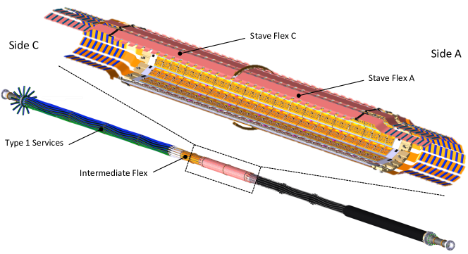
The ATLAS ID, including the IBL detector and its envelope, is shown in Figure 1. The 3-dimensional structure of the IBL detector with its services is shown in Figure 2.
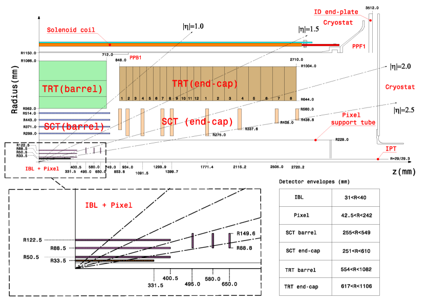
The main IBL layout parameters are summarised in Table 1 and a comparison between the technical characteristics of the IBL and the Pixel detector is shown in Table 2. With a mean sensor radius of (compared with for the Pixel B-Layer), the IBL sensors and front-end electronics must cope with a much higher hit rate and radiation doses of NIEL and 250 MRad TID during Phase-I operation. To address these requirements, a new front-end read-out chip, the FE-I4B [8], was developed in CMOS technology satisfying the ATLAS requirements of radiation tolerance and read-out efficiency at high luminosity. In addition, the FE-I4B chip has a substantially larger active area compared to the FE-I3 front-end chip [4] of the Pixel detector, and a cell size reduced to from , the shorter side being in the transverse plane. The smaller layer radius and the reduced pixel cell length are crucial parameters in defining the performance improvement of the ID, in particular the track-extrapolation resolution.
| Item | Value |
|---|---|
| Number of staves | 14 |
| Number of physical modules per stave | 20 (12 planar, 8 3D) |
| Number of FEs per stave | 32 |
| Coverage in , no vertex spread | |
| Coverage in , 2 () vertex spread | |
| Active stave length () | 330.15 |
| Stave tilt in (degree) | 14 |
| Overlap in (degree) | 1.82 |
| Center of the sensor radius () | 33.5 |
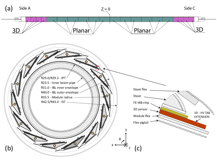
The IBL stave configuration is shown in Figure 3. Two module types [9] are installed on each stave. A total of 12 double-chip planar n-in-n sensors similar to those equipping the Pixel detector, each bump-bonded to two FE-I4B read-out chips, populate the central stave region. Four single-chip 3D sensors, adopted for the first time in a collider tracking detector and each bump-bonded to one FE-I4B chip, populate each end of the stave. The staves are mounted with the sensors facing the beam pipe and are inclined in azimuth by to achieve an overlap of the active area. This tilt also compensates for the Lorentz angle of drifting charges in the case of planar sensors, and the effect of partial column inefficiency for normal incidence tracks in the case of 3D sensors. Owing to space constraints, the sensors are not shingled along the stave (in ). To minimise the dead region, modules are glued on the stave with a physical gap of .
| Technical characteristic | Pixel | IBL |
| Active surface () | 1.73 | 0.15 |
| Number of channels (x 106) | 80.36 | 12.04 |
| Pixel size () | 50400 | 50250 |
| Pixel array (columns rows) | 16018 | 33680 |
| Front-end chip size () | 7.610.8 | 20.219.0 |
| Active surface fraction () | 74 | 89 |
| Analog current () | 26 | 10 |
| Digital current () | 17 | 10 |
| Analog voltage () | 1.6 | 1.4 |
| Digital voltage () | 2.0 | 1.2 |
| Data out transmission () | 40-160 | 160 |
| Sensor type | planar | planar / 3D |
| Sensor thickness () | 250 | 200 / 230 |
| Layer thickness () | 2.8 | 1.88 |
| Cooling fluid | C3 F8 | CO2 |
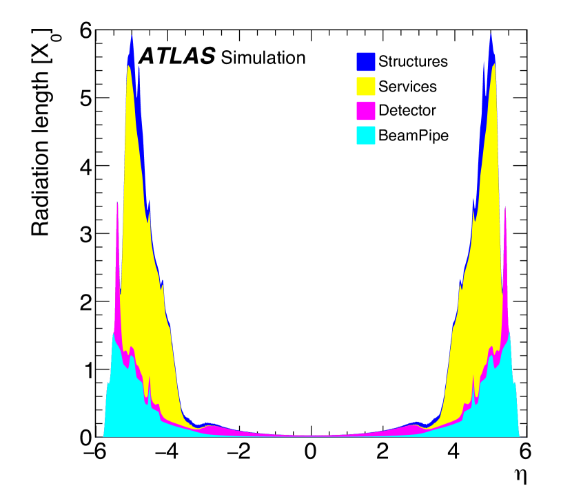
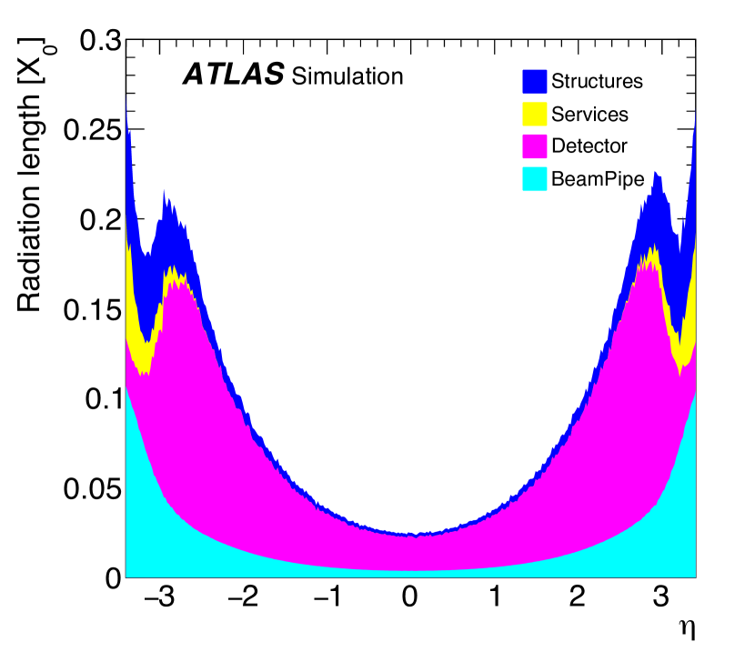
Minimising the material budget is very important for the optimisation of the tracking and vertex performance. The IBL radiation length, averaged over azimuth and taking into account the stave tilt and the overlap between staves, is estimated to be 1.88% X0 for tracks produced perpendicular to the beam axis at . This is less than that of the Pixel B-Layer333The as-built IBL radiation length was evaluated using the ATLAS geometry model, as discussed in the IBL TDR [6]. The difference with respect to the value reported in the IBL TDR is mainly due to an initial underestimation of the module material and the addition of the IPT. A recent description of the ATLAS ID material and its comparison with Run 2 collision data is now available [10].. The reduced thickness was achieved by using more advanced technologies as discussed in the following sections. These include: a new low-mass module design; local support structures (staves) made of low density, thermally conductive carbon foam; the use of CO2 evaporative cooling, which is more efficient in terms of mass flow and pipe size; and electrical power services using aluminium conductors. Table 3 reports the main contributions to the IBL material budget. Figure 4 shows the material traversed by a straight track originating in as a function of , smeared over the azimuthal angle.
| Item | Value () |
|---|---|
| Beam pipe | 0.32 |
| IPT | 0.12 |
| Module | 0.76 |
| Stave | 0.60 |
| Services | 0.19 |
| IST | 0.21 |
| IBL total | 1.88 |
2.2 System overview
The IBL electronic system includes the FE-I4B read-out chip, the off-detector read-out boards (the read-out driver (ROD) [11] and the back-of-crate board (BOC) [12, 13]), the detector control system (DCS) [14], the electronics and sensor power supplies, and all of their associated electrical and optical services. The data acquisition (DAQ) [15] controls the transfer of data to and from the off-detector read-out boards, while the DCS controls the electrical and environmental monitoring of the detector as well as the power distribution to the pixel sensors and FE-I4B chips.
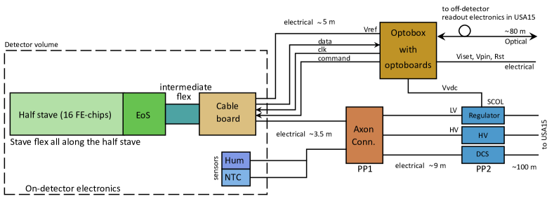
The electrical service design was driven by physical space constraints, especially in the inner region where all services and connectors must fit into the narrow IBL envelope over a length of approximately , and by the conflicting requirements of material budget, radiation hardness and electrical performance. Optical transmission is excluded in the IBL envelope because of the high radiation level. Figure 5 shows a block diagram of electrical services for one half-stave (the services are symmetrical, at each end of a stave). Each module of a given half-stave is connected electrically by a stave flex to an end-of-stave (EoS) card. The stave flex transfers the data from the half-stave, as well as control signals from the DAQ and DCS, and the power distribution. In the EoS region the detector services are connected via intermediate flexes to a cable board. The cable board connects the flexes to -long extensions (Type 1 cables) that reach the ID end-plate where the first Patch Panel (PP1) is located to allow for electrical and optical connections to the external services after installation in ATLAS. A second break of the electrical services occurs at another Patch Panel (PP2) on the detector periphery that is accessible during a short shut-down.
Details of the FE-I4B chip and the module flex hybrid that connect a module to the stave flex are described in Section 3, while those of the stave flexes are described in Section 4. The off-detector electronics and power-supplies, as well as the electrical and optical services, are described in Section 6.
2.3 Tracking and flavour tagging performance
The ATLAS ID provides charged particle tracking with high efficiency in the range over the full azimuthal range. The pixel layers are crucial for the reconstruction of charged particles trajectories, for their extrapolation to the production point and for the reconstruction of multiple collision and decay vertices which occur in each bunch crossing. The pixels are therefore of crucial importance to the flavour tagging performance. Any inefficiency of the innermost B-Layer would result in a degradation of that performance.
A first assessment of the expected improvements in tracking and vertex reconstruction performance was performed for the IBL Technical Design Report (TDR) [6]. Since then, the ATLAS simulation, digitisation and cluster reconstruction algorithms have been refined and improved.
The IBL improves the track extrapolation resolution with respect to the Pixel detector of Run 1 by providing an additional high-precision hit closer to the interaction point. This is particularly important for low particles, where it mitigates the effect of multiple scattering in the detector material on the track extrapolation, thus improving the impact parameter resolution in both the transverse () and longitudinal () projections. The smaller pixel pitch of the IBL in the longitudinal direction contributes to improving the resolution in across the full spectrum.
The track reconstruction performance has been evaluated using Monte Carlo simulations of events, comparing the Run 1 detector geometry to a geometry including the IBL, while keeping all other conditions unchanged. An improvement in the resolution of approximately 2 (1.5) for tracks with of 1 (100) GeV is observed following the addition of the IBL. In the transverse direction, the addition of the IBL improves the resolution by a factor of approximately 2 for tracks with of 1 GeV, with the resolutions for the two geometries converging beyond 10 GeV. These results are confirmed by comparing the track impact parameter resolution measured in Run 1 (2012) data with that in Run 2 (2015) data [16].
In addition to the charged particle track reconstruction, these improvements enhance the primary vertex reconstruction and resolution, the secondary vertex finding, and the flavour tagging performance, hence considerably extending the physics reach of ATLAS analyses.
The IBL also helps to maintain the performance and robustness of the ID track reconstruction when the B-Layer read-out efficiency deteriorates at high peak luminosity, or after a large integrated luminosity (radiation damage to the sensors and front-end electronics as well as possible irreparable failures of its chips and modules).
The flavour tagging performance expected with the addition of the IBL is evaluated using a more realistic simulation of the ATLAS ID based on the final IBL geometry, an updated digitisation model and improved reconstruction algorithms with respect to the IBL TDR. The latter include a refined neural network clustering algorithm [17], a new tracking configuration, which improves the treatment of shared clusters in the core of a dense jet environment [18] and new flavour tagging algorithms. These results supersede those presented in the IBL TDR. Results are based on fully simulated production events at a collision energy of 13 TeV. The average level of pile-up is approximately 20, reflecting the Run 1 luminosity profile. Jets used for flavour tagging are reconstructed using the anti- algorithm [19] with radius . ATLAS combines the discriminating variables obtained from impact parameter, inclusive secondary vertex and multi-vertex reconstruction algorithms. A detailed description of these algorithms can be found in reference [20].
The combination of the input variables obtained from these algorithms is obtained using a boosted decision tree (MV2c20) [21]) that returns a continuum variable peaked around 1 for jets likely to contain a -flavoured hadron and around for those likely to originate from light-flavoured quarks. This MV2c20 is an evolution of the neural network algorithm used during Run 1 [20]. In order to perform an useful comparison, the MV2c20 algorithm has been separately re-trained for the sample generated using the ATLAS Run 1 geometry, without the IBL, and the ATLAS Run 2 geometry, which includes the IBL.
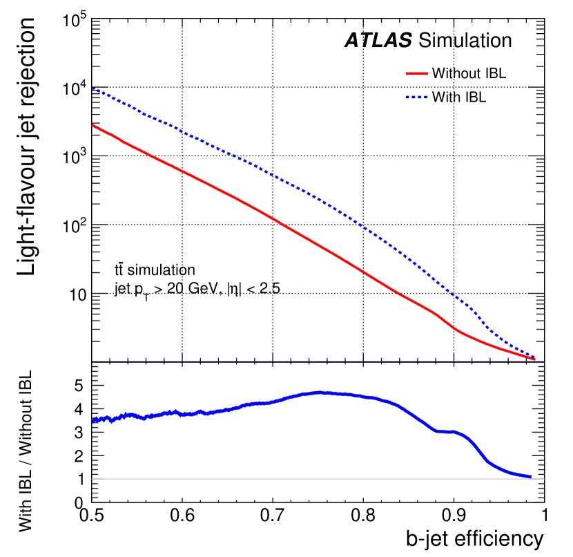
Figure 6 shows the light-jet and -jet rejection as a function of the -jet purity obtained with the two configurations. The addition of the IBL improves the light-jet (-jet) rejection by a factor up to 4 (1.8) for -jet tagging efficiencies up to 85%. Physics analyses will most often profit from the improved performance by re-tuning their -tagging requirements in such a way to keep a similar background rejection with an increased signal efficiency. The improvement in performance at constant rejection is summarised in Table 4 for different working points.
| light-jet rejection | -jet efficiency | -jet efficiency |
|---|---|---|
| without IBL (%) | with IBL (%) | |
| 1000 | 57 | 65 |
| 100 | 71 | 79 |
| 10 | 84 | 90 |
| -jet rejection | -jet efficiency | -jet efficiency |
| without IBL (%) | with IBL (%) | |
| 20 | 56 | 62 |
| 10 | 63 | 68 |
| 5 | 72 | 76 |
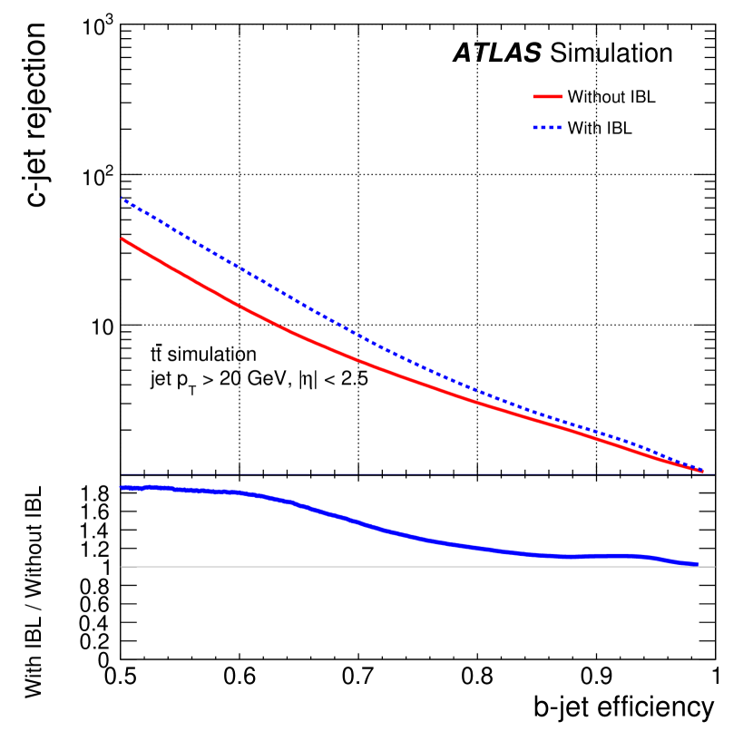
The -tagging performance as a function of jet is shown in Figure 7. The largest improvements are seen at low values of the jet where the proximity of the IBL to the interaction region significantly reduces the impact of multiple scattering in the track reconstruction. The improvement in light-jet (-jet) rejection ranges reaches a factor 4 (1.6) for jet 100 GeV while at higher the tracking performance gain is limited by shared clusters from collimated tracks produced in the core of high jets.
3 Modules
The basic building block of the IBL detector is the module. For each beam crossing an FE-I4B read-out chip records, digitises and locally stores the data from a silicon sensor that is connected to it. Two sensor technologies are used: planar and 3D. A planar silicon wafer contains four sensor tiles, each of nominal dimension ( in the production process after dicing). A 3D silicon wafer contains eight sensor tiles, each of dimension . There are consequently two module types, planar and 3D:
-
-
A planar module consists of a planar sensor tile connected to two FE-I4B chips. Each chip consists 26880 pixel cells having analog and digital circuitry arranged in a matrix of 80 columns of pitch and 336 rows of pitch. Each FE-I4B cell is bonded using Sn/Ag bumps to a corresponding cell of the planar tile;
-
-
A 3D module consists of a 3D sensor tile connected to a single FE-I4B chip with each cell of the FE-I4B chip bonded to a corresponding cell of the 3D tile;
-
-
A double-sided, flexible printed circuit (the module flex hybrid) connects the module to external electrical services.
The sensor design, production and yield is discussed in Section 3.1. This is followed by a discussion of the FE-I4B production and yield in Section 3.2. The module hybridisation, that is the bump-bonding of the FE-I4B chip(s) and a wafer to produce a bare module, is made industrially. A module flex hybrid is then attached at module production sites to the bare module, prior to detailed performance studies of the final (dressed) module. The module hybridisation, the module flex hybrid connectivity and the final performance are described in Sections 3.3 and 3.4. Finally, the overall module production yield is summarised in Section 3.5.
3.1 Sensors
Two sensor technologies are used for IBL modules. The planar sensor is a development of the Pixel detector sensor design, with several improvements. Most notably, since the limited IBL clearance precludes sensor shingling along the staves (as in the Pixel detector), the inactive sensor edges are substantially reduced to minimise efficiency losses. The 3D sensor design [22] is a new technology developed for increased radiation hardness, and relies on columnar electrodes penetrating the substrate, reducing the drift path with respect to the planar approach while keeping a similar thickness and thus signal size. As discussed in detail in reference [9], both sensor types show satisfactory test-beam performance in terms of noise, hit efficiency and hit uniformity for a fluence of up to . An effective inactive edge width of () was measured for planar (3D) sensors.
The planar n+-in-n sensors have proven their excellent performance during the Run 1 operation of the Pixel detector and are a well-developed technology. Nevertheless, the 3D sensors have a potentially important advantage in terms of power consumption after high radiation because of their lower operating voltage.
Double-chip planar sensor modules cover the central region of the detector, of the active area, while the high regions are populated by single-chip 3D sensor modules. This mitigates the reduced efficiency measured for normal incidence in the region of the 3D sensor electrodes.
3.1.1 Planar design
The design of the planar IBL sensor is an evolution of the Pixel detector sensor [4] with n+-in-n pixels. The n-side segmentation matches in size the FE-I4B read-out electronics connected via bump-bonds; a guard-ring structure is placed on the p-side. The planar IBL double-chip sensors are produced at CiS444CiS Forschungsinstitut fr Mikrosensorik und Photovoltaik GmbH, Erfurt (Germany)., using n-type wafers of diameter and thickness, with resistivity in the range and a crystal orientation. Each wafer contains four sensor tiles of mean dimension after dicing. Details of the sensor design can be found in reference [23]. Key features include slim edges achieved by stretching the edge pixel size opposite to the guard-rings to , possible in n+-in-n sensors because of the double-sided process; this option was implemented after extensive studies of the sensor efficiency in the peripheral area [24]. The number of guard-rings was optimised based on a complementary study, which evaluated the breakdown behaviour after partial guard-ring removal [25]. Compared to the Pixel detector sensor, the number of guard-rings has been reduced from 16 to 13 and the cutting edge has been moved closer to them, as indicated in Figure 8 where the overall reduction of the inactive edge (from 1100 to ) is shown.
(a) 
(b) 
The nominal pixel size is by pitch, matched to that of the FE-I4B chip. The two central columns of these double-chip sensors are extended to rather than to cover the gap between the two adjacent FE-I4B chips.
3.1.2 3D design
In 3D pixel sensors, the columnar electrodes penetrate the substrate instead of being implanted on the wafer surface. The depletion electric field is therefore parallel to the wafer surface. The position and doping of the wide columns define the pixel configuration; the distance between electrodes can be typically fives times smaller than the sensor thickness, thereby dramatically reducing the charge-collection distance and depletion voltage. Although the fabrication process of 3D sensors is more complex, significant advantages can potentially be realised by independently controlling the drift distance and the sensor thickness. Because of the low depletion voltage, the power dissipation per unit leakage current is reduced. The cooling requirements are therefore less demanding. The signal size is determined by the sensor thickness, independently of the small drift distance. Furthermore, the drift perpendicular to the track direction results in fast signals, which are robust against charge trapping caused by heavy radiation damage [22].
The IBL 3D sensors were fabricated at FBK555Fondazione Bruno Kessler, Povo di Trento (Italy). and CNM666Centro Nacional de Microelectronica, Barcelona (Spain). with a double-sided technology [26, 27]. Starting from p-type Float Zone wafers of diameter and thickness, with high-resistivity (10 to ) crystalline silicon and orientation, columnar electrodes of diameter were obtained by Deep Reactive Ion Etching (DRIE) and dopant diffusion from both wafer sides, without the presence of supporting wafers. By doing so, the substrate bias can be applied from the back side (p+), as in planar devices. Figure 9 shows details of the 3D column layout.
Each pixel contains two read-out (n+) columns (two-electrode configuration), with an inter-electrode spacing between n+ and p+ columns of . In order to maintain a reasonable yield, each wafer contains eight sensor tiles of dimension , rather than the four larger sensor tiles of the planar design. A wide region separates the active pixel area from the physical edge of the tile.
The main differences between FBK and CNM 3D sensors are the following:
- -
-
-
in FBK sensors, the surface isolation between n+ electrodes is obtained by a p-spray layer on both wafer sides, whereas in CNM sensors, p-stops are used on the front side (n+) only;
-
-
the edge isolation in FBK sensors is based on multiple rows of ohmic columns stopping the lateral spread of the depletion region [30], whereas in CNM sensors a 3D guard-ring, surrounded by a double row of ohmic columns, is used to sink the edge leakage current.
Table 5 summarises the main parameters of the IBL sensors.
| Parameter | Planar | 3D FBK | 3D CNM |
|---|---|---|---|
| Tile dimension [] | 41315 18585 | 20450 18745 | 20450 18745 |
| Sensor thickness [] | 200 | 230 | 230 |
| Sensor resistivity [] | |||
| Pixel size (normal) [] | 250 50 | 250 50 | 250 50 |
| Pixel size (tile edge) [] | 500 50 | 250 50 | 250 50 |
| Pixel size (tile middle) [] | 450 50 | - | - |
| Edge isolation | Guard-rings | Fences | 3D guard-ring, fences |
| Pixel isolation | p-spray | p-spray | p-stop on n-side |
| Nominal operating bias voltage [] | / | / | / |
| (non-irradiated / ) | |||
| Maximum operational power [] | 90 | 15 | 15 |
| ( and ) |
3.1.3 Sensor production and quality assessment
The electrical quality of the sensors was evaluated from the measurement of the current-voltage (I-V) dependence, as this is sensitive to bulk and surface defects. Tiles satisfying the selection criteria described below were chosen for hybridisation (connection between the sensor and the FE-I4B read-out electronics).
The planar design includes a grid structure that allows biasing of the entire sensor by means of a punch-through technique [31]. This bias grid was used to evaluate the quality of the tiles before the sensors were connected to the read-out electronics with the bump-bonding process. After bump-bonding the pixels were biased through the FE-I4B chip while the bias grid, connected to ground via a special bump in the periphery of the pixelated region, was not in operation.
The leakage current of the planar tile, evaluated at an operating voltage (V) below the depletion voltage (V), was required to be I(V) < , and the slope of the I-V curve was limited to I(V)/I(V) < 1.6. Wafers with two or more planar tiles that satisfied this requirement were sent for under-bump metallisation (UBM) and dicing at IZM777Fraunhofer IZM, Gustav-Meyer-Allee 25, 13355 Berlin, Germany.. The yield of the planar production (the percentage of planar tiles satisfying the above criteria) before under-bump metallisation and dicing was .
Due to the difficulty of implementing a bias grid structure compatible with the 3D design, alternative evaluation methods were developed for 3D sensors:
-
-
FBK sensors include a metal grid connecting all pixels in each column to a pad located in the periphery of the active region. By measuring the I-V curves of the 80 columns with a specially designed probe card, the quality of each sensor on the wafer can be evaluated. The metal layer was removed by chemical etching after the I-V measurement and the wafers with three or more selected tiles were sent to IZM for UBM and dicing. The sensors that passed the selection criteria were bump-bonded to read-out chips. The sensors were required to have a breakdown voltage V < , V > and I(V) < where V = V. The slope of the I-V curve was also constrained to satisfy I(V)/I(V) < 2. The sensor yield of the FBK production on the selected wafers was .
-
-
The CNM sensor selection criteria were initially based on the leakage current measured through the 3D guard ring structure surrounding the pixelated area. While the p-side of the wafer was biased, the 3D guard ring was connected to ground via a dedicated pad, and the I-V curve was measured for each sensor before the wafer dicing. After hybridization, the 3D guard ring was connected to ground through two special bumps of the FE-I4B chip. The CNM sensors were required to satisfy V < , V > and I(V) < with V = V. I is the leakage current measured on the 3D guard ring. The slope of the I-V curve was required to satisfy I(V)/I(V) < 2. Wafers with at least three sensors passing the selection criteria were sent to IZM for UBM and dicing. Initial studies indicated a good correlation between V measured through the 3D guard ring structure and that after detector assembly [9]. However, during module assembly, the correlation proved to be poor, with several CNM 3D modules showing a low V. This was because of defects located in the central volume of the sensor that do not affect the region probed by the 3D guard ring.Once this lack of correlation was established, all CNM sensors that were not assembled were re-tested on a probe station. The n-side of the sensor was placed in contact with a grounded chuck via the under-bump metallisation (Section 3.3.1), while the p-side was connected to the bias potential. Those sensors satisfying V < were selected for hybridisation. The sensor yield of the CNM production on the selected wafers, as measured with the 3D guard ring method, was . However, after re-testing, the final CNM production yield was similar to that for FBK wafers.
3.2 On-detector electronics
3.2.1 The FE-I4 front-end chip
The FE-I4B front-end chip was developed for the IBL read-out. A first version, the FE-I4A [8, 32], was fabricated in 2010 and used to develop and validate the IBL module design [9]. The FE-I4A was not intended for the final detector and the pixel matrix was non-uniform to allow performance comparisons between various analog circuit design choices. The FE-I4B chip was first fabricated in 2011 [33, 34] and tailored to fully meet the IBL requirements. In addition to selecting the analog design and making the pixel matrix uniform, specific powering choices were made and data acquisition features added.
The FE-I4A and FE-I4B both contain read-out circuitry for ybrid pixels arranged in 80 columns of pitch by 336 rows of pitch. Each FE-I4 pixel contains a free running clock-based amplification stage with adjustable shaping, followed by a discriminator with an independently adjustable threshold. The chip keeps track of the time stamp for each discriminator as well as the 4-bit Time over Threshold (ToT)888 The Time over Threshold is defined as the time the amplifier output signal stays above threshold, measured in units of the LHC clock (25 ns). This quantity is related to the collected charge.. Information from all firing discriminators is kept in the chip for a latency interval programmable up to 255 LHC clock cycles of 25 ns, and is retrieved if a trigger is supplied within this latency. The IBL data output is a serial Low Voltage Differential Signal (LVDS), 8b/10b encoded at a rate of . The chip has many configurable settings that are stored in triple-redundant registers providing the required radiation hardness to single event upsets (SEU) [35].
Because of space and material limitations, the IBL FE-I4B chips are powered from a single DC supply over long cables providing a resistive load. The single voltage feeds two Shunt-LDO999A shunt combined with a Low-Drop-Out regulator. voltage regulators [36, 37] drawing a minimum standing current of even when the chip is neither clocked nor configured. This limits the amplitude of voltage transients resulting from current changes on the resistive supply lines, particularly important since the difference between the nominal and maximum input voltage ratings is small. The regulators and attendant voltage references have an input voltage limit of , compared with nominal operation at . Once the chips are configured and clocked, and their internal current draw exceeds , the regulator shunt elements shut off and draw no additional current. The chip operates internally with two voltage rails generated by the regulators, nominally for the analog circuitry and for the digital circuitry. Both voltages are adjustable with a hard-wired maximum around (which varies slightly from chip to chip). The voltage references use a combination of a programmable current reference (feeding a poly-silicon resistor) and a fixed voltage reference. This combination was chosen to allow reliable start-up at low temperature (as low as ), as well as excellent stability (< ) up to high radiation dose ().
Several features important for IBL operation were introduced in the FE-I4B design following experience with prototype FE-I4A modules. Some details of the analog bias distribution and charge injection were changed to correct for degradations observed in the FE-I4A after the expected IBL lifetime dose, particularly at low temperatures. A programmable event-size limit was introduced to avoid data acquisition time-outs from occasional pathologically large events. Bunch crossing and trigger counters were increased to respectively 13 and 12 bits, to avoid ambiguities in tracking the state of each chip. Improved diagnostics were implemented to count and report any skipped triggers (the chip will skip any triggers received when the 16-bit trigger buffer is full).
3.2.2 FE-I4B production and quality assessment
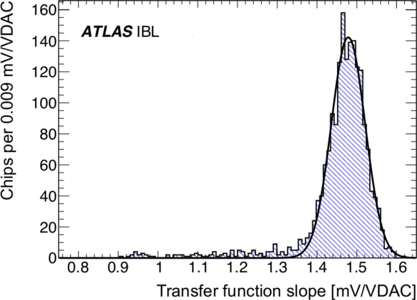
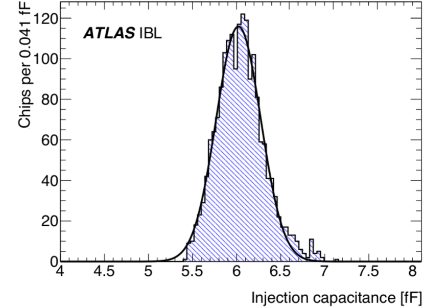
For the IBL production, FE-I4B chips on fifty-one diameter wafers were tested. The data acquisition and handling were performed with a custom read-out system [4, 38]. A custom PCB was used to interface the read-out system hardware with a probe card, establishing electrical contact with 108 FE-I4B pads. All 60 chips of a wafer were probed with an average measurement time of 2.5 days. The goal was to identify FE-I4B chips that were suitable for the IBL and to measure their calibration constants. For chip calibrations it was necessary to make contact with dedicated FE-I4B pads not wire-bonded on the IBL read-out circuit. The chip calibrations were therefore only possible at wafer level. Two calibration constants of the internal charge injection circuit are shown in Figure 10. The circuit distributes a voltage step to injection capacitors present in each pixel and is needed to tune the FE-I4B chips during IBL operation. On average for the accepted chips, the injected charge changes with the value (VDAC) of the injection circuit digital-to-analog converter (DAC) setting approximately as
to provide a transfer function between the value of the DAC setting and the signal.
More than 50 tests were used to evaluate the chip response to charge injection, the functionality of digital hit processing, the chip configurability, and the power consumption. Approximately 18000 values were recorded per wafer. A custom made software designed for wafer and module tests of the IBL production was used to automatically determine the chip status. The selection criteria were defined after the distributions of the first ten wafers were studied. A detailed description of the tests and selection criteria is available elsewhere [39].
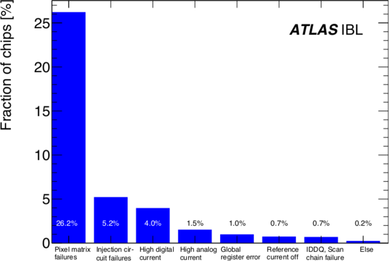
Test results of 2814 fully probed chips are listed in Figure 11. In addition, 246 chips ( of all chips) were not fully probed because of an anomalous high current at start-up (dead-shorts). Additional IDDQ101010Measurement of the supply current (Idd) in the quiescent state., Scan chain and Shmoo plot111111A plot showing the range of conditions (voltages, temperatures and inputs) in which the chip operates. tests were made by an external company for the first afers, but the failure rate was low (less than ). In total, 1821 chips () were qualified for IBL module assembly.
Since the powering scheme was not finalised at the time of wafer testing, the on-chip power regulators of the FE-I4B chips were only tested after the module assembly (Section 3.4).
3.3 Module assembly
3.3.1 Hybridisation of the FE-I4B chip and the sensor
The connection between sensor and electronics was achieved using fine-pitch bump-bonding and flip-chip technology. This was already used with a pitch for the construction of the Pixel detector modules [4]. The IBL modules use a similar electroplated (SnAg) bumping process provided by IZM. The bumping process is divided into three steps: under-bump metallisation (UBM) on the sensor and FE-I4B wafers; solder bump deposition on the FE-I4B wafers; and a flip-chip of the diced FE-I4B chips and sensors. The UBM is necessary due to the non-solderable aluminium pads on the sensors and FE-I4B chips; the UBM metal stack consists of electro-deposited Cu on top of a sputtered Ti/W adhesion layer. Solder bumps are then deposited on the FE-I4B wafers using electroplating only. The flip-chip operation follows the dicing of the sensor wafers. The FE-I4B chip is placed on the sensor substrate with high accuracy and the assembly is soldered to form the electrical and mechanical interconnection in a reflow soldering process. The sensor bonded to the FE-I4B chip(s) is commonly referred to as a bare module.
The procedure was modified with respect to that used for Pixel modules to suit the dimensions of the IBL module components. The FE-I4B chip covers an area of 20.27 and was thinned to before bump-bonding. Unconstrained, the thinned FE-I4B would undergo a distortion exceeding during the high temperature reflow soldering phase, which would result in unconnected bumps especially in the outer areas of the assemblies. To avoid this, a temporary -thick sapphire glass handle wafer was bonded to the FE-I4B chip before UBM. A polyimide bonding technique allowed a laser-induced debonding of the glass carrier at room temperature after dicing and flip-chipping. This debonding process used an UV excimer laser with a wavelength of traversing the glass carrier to the bonding interface. The glass carrier was optimised to ensure that the laser light was fully absorbed in the polyimide bonding layer, thus releasing the FE-I4B chips.
Only of the chip length is dedicated to End-of-Column (EoC) logic outside the active pixel matrix. The size is determined by the need to wire bond the I/O and power pads to the read-out chip with the bump bonded sensor in place. The chip-level logic and global configuration occupy less than of the periphery. Once bonded, most of the EoC part extends beyond the sensor area so that the wire bonding pads at the output of the EoC logic are still accessible to connect the read-out chip via aluminium-wire wedge bonding.
3.3.2 Module flex hybrid
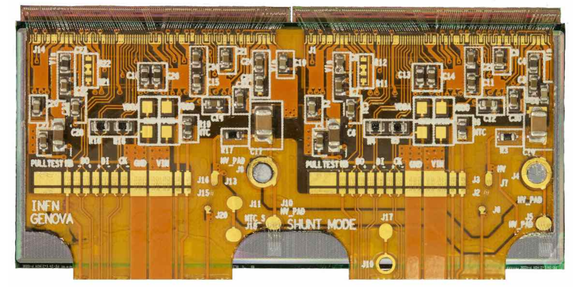
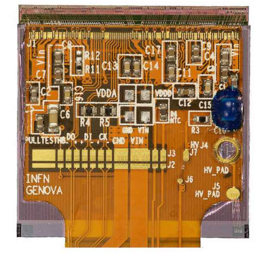
The module flex hybrid is a double-sided, flexible printed circuit board which routes the signal and power lines between the stave flex hybrid and the FE-I4B chips, holds the required passive components, and routes the bias voltage to the sensor via Cu traces. Figure 12 shows a photograph of the module flex hybrids for single-chip and double-chip modules. The envelope of the module flex hybrid is defined by the sensor dimensions and it is slightly narrower than the sensor width.
The module flex hybrids are glued to the back side of the sensor and connected to the longitudinal stave flex, which is located at the back side of the stave, via thin transversal wings, one per read-out chip (Section 4.2). The -thick flex stack consists of two -thick copper layers embedded in dielectric polyimide sheets, glued with acrylic adhesive. Passive components are soldered on the module flex hybrid for the FE-I4B chip decoupling, power supply and HV filtering, and for terminations of the signal traces. The module temperature monitoring and interlock is made via a Negative Temperature Coefficient thermistor (NTC) mounted on the module flex hybrid. All passive components are soldered on the top layer of the module flex hybrid. Special emphasis is given to HV routing and filtering since the flex hybrid must be functional up to . To avoid HV discharges, wider spacing between the HV traces and the data and LV traces is introduced. The HV capacitor is encapsulated with a polyurethane resin and thick Kapton®121212Kapton® is a Dupont Corp. trademark for polyimide films, see http://www.dupont.com. cover layers are used on the top and bottom of the flex hybrid.
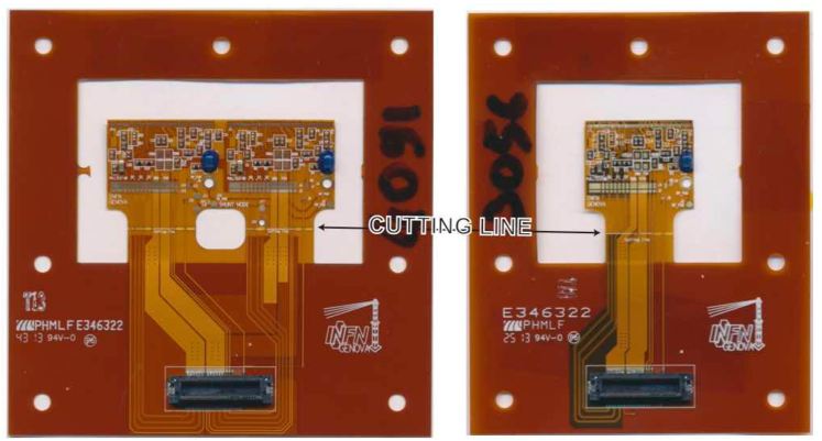
All signal and power traces of the module flex hybrid are routed to a connector on a frame outside the module area that is used during the module production QA. A temporary wire bond connection is necessary to connect all signal and power lines from the flex to the connector on the frame. Prior to the loading of the module to a stave the connector area is cut away. The cutting line is approximately from the sensor.
The module flex hybrids were produced by Phoenix S.r.l.131313Phoenix S.r.l., Via Burolo 22, 10015 Ivrea (Torino), Italy. and the surface mount component loading and encapsulation was made by Mipot S.p.A.141414Mipot S.p.A., Via Corona 5, 34071 Cormons (Udine), Italy.. Basic QA operations such as testing of line integrity for open and shorted connections were made by the vendors and were followed by more detailed tests at the two module assembly sites. These procedures included HV standoff tests at , visual inspection and dedicated cleaning to allow for high-quality wire bonding.
3.3.3 Final module assembly
The final (dressed) module assembly was made at two module production sites in the period 2012 to 2014, following four assembly steps described below.
A detailed visual inspection of the module flex hybrid was initially made, together with electrical tests of the line and pad integrity, and the hybrid components. To ensure a good wire bonding performance, the flex hybrid was then cleaned in an ultrasonic bath, rinsed with distilled water, and dried. The visual inspection was then repeated.
A visual inspection of the bare module was made to identify scratches or other damage. For planar double-chip modules a re-measurement of the I-V was made to check the sensor quality. Thirteen planar modules () and eight 3D modules () were rejected.
The key assembly step is the alignment and attachment of the bare module and the module flex hybrid. The module flex is glued on the sensor back-side. For this reason, it is necessary to visually access the sensor alignment marks, and to be able to wire-bond to both the FE-I4 chip and the flex wings. An alignment precision of order is required. The alignment and gluing procedure differed slightly between the production sites, and the detailed jig designs were developed autonomously. Separate alignment jigs were developed for the planar double-chip and 3D single-chip modules. Several jig sets were made to ensure production capacity, but the module assembly rate was in fact determined by the component supply. Both the module flex and the bare module were initially aligned on separate jigs using alignment marks, and fixed in place via vacuum. The module flex was then removed with a special jig, maintaining the alignment position but allowing access for the deposition of glue. The jig was designed to protect the hybrid components. Glue patterns were then deposited on the flex hybrid: a double tape strip (PPI RD-577F151515PPI RD-577F®, PPI Adhesive Products GmbH, see www.ppi-germany.de. or ARclad161616ARclad®, Adhesives Research Corp., see www.adhesivesresearch.com.) was placed underneath the FE-I4B wire bond pads, and epoxy glue patterns (UHU EF 300171717UHU EF 300®, UHU GmbH, see www.uhu.com. or Araldite 2011181818Araldite® is a trademark of Huntsman Advanced Materials, see ) were placed under the remainder of the module flex hybrid, especially under the wire bond bridge area and the HV connection pads. The jigs were then aligned and brought into contact. Pressure was applied on the assembly, and in particular around the critical wire bond regions, during curing.
The final step was the wire bonding of the FE-I4B chip and sensor to the module flex hybrid and of the wire bond bridge to the test connector (Section 12), using -thick aluminium wire (at least three wire bonds were applied to the low- and high-voltage pads for redundancy and safety). Wire bond pull tests were consistently recorded to ensure the bond integrity.
At each stage of the assembly, details of the module components, as well as metrology and bonding information, were recorded. No site dependence of the module quality was identified.
Fully dressed planar (double-chip) and 3D (single-chip) modules are shown in Figure 13. Table 6 summarizes the material budget (units of radiation length for normal incidence) of the IBL modules; the contributions of the different components are averaged over the active module area.
A total of 688 fully dressed modules (410 planar, 162 3D CNM and 116 3D FBK) were delivered for module testing, tuning and characterisation.
| X/X0() | ||
|---|---|---|
| Total FE-I4B + bumps | 0.21 | |
| FE-I4B chip | 0.20 | |
| Bump-bonds | 0.01 | |
| Planar (3D) sensor | 0.24 (0.27) | |
| Total module flex hybrid | 0.13 | |
| Cu traces | 0.076 | |
| Polyimide/epoxy | 0.028 | |
| SMD components | 0.025 | |
| Total planar (3D) module | 0.58 (0.61) |
3.4 Module performance and quality assurance
| Test Name | Test Purpose | Test stage |
|---|---|---|
| Sensor current vs. applied bias voltage | Sensor operability and | Q, F |
| reference characteristics measurement | ||
| Power-up test | Chip supply voltage and current test | Q, F |
| Shunt-LDO I/V scan | Shunt-LDO warm/cold calibration | Q, F |
| and functionality test | ||
| Generic ADC test | Generic ADC warm/cold calibration and | Q, F |
| Shunt-LDO calibration verification | ||
| Sensor bias ON | Ramp-up of sensor depletion bias | Q, F |
| Digital test (high threshold) | Pixel read-out chain functionality | Q, F |
| Module tuning | Multi-step threshold and feedback | Q, F |
| current adjustment (global and pixel level) | ||
| Digital test (operation threshold) | Pixel digital read-out chain functionality | Q, F |
| Analog test (operation threshold) | Pixel analog read-out chain functionality | Q, F |
| Threshold and noise measurement | Threshold and noise (ENC) measurement | Q, F |
| ToT verification at the charge | Charge measurement verification | Q, F |
| of (MIP) | ||
| Crosstalk test | High analog charge injection | Q, F |
| for inter-pixel crosstalk test | ||
| t0-tuning | Injection timing fine adjustment | F |
| In-time threshold measurement | Threshold for hit detection within | F |
| single bunch crossing measurement | ||
| ToT calibration | Full range ToT to charge calibration | F |
| Noise occupancy measurement | Noise hit probability at operation threshold | F |
| and noisy pixel masking | ||
| Source scan | 241Am high statistics source scan | F |
| for bump connectivity test | ||
| Low threshold operability test | Noise occupancy as function | F |
| of threshold measurement | ||
| Sensor bias OFF | Ramp-down of sensor depletion bias | Q, F |
| Threshold and noise measurement | Threshold and noise (ENC) measurement | Q, F |
| with undepleted sensor to detect defective bumps |
Prior to the loading of modules onto a stave, each module was tested to ensure its mechanical and electrical functionality, its tolerance to environmental stress, and its electrical performance. The performance validation identified both module-level failures and pixel-level failures. Modules were selected for stave loading on the basis of this validation and only modules passing all tests were selected. At the pixel level, any pixel that failed at least one electrical test was recorded and modules with a bad pixel count of more than were rejected. The bad pixel category also included bad pixels resulting from nonconformities such as re-work, sensor scratches or the chipping of electronic components.
An initial electrical verification, including the sequential room-temperature tests labelled Q in Table 7, was performed after the module assembly. Modules accepted by this initial test were then subjected to an environmental stress test of thermal cycles between and . The modules were not powered during the thermal cycles. Seventy-three modules ( of those delivered) were rejected at this stage because of major mechanical or electrical failure, a large fraction being due to a defective on-chip power regulator on the FE-I4B chips. As noted in Section 3.2.2, the power regulators were not tested at the wafer level.
An extensive validation stage was then made for each module at both the module and individual pixel level. This included the sequential tests labelled F in Table 7. The different measurements are described in Sections 3.4.1 through 3.4.5.
A measurement of the sensor I-V was initially made at room temperature with a requirement on the breakdown voltage (V) depending on the module type. Modules failing the V requirement were rejected. A detailed electrical calibration and characterisation was then made at the foreseen detector operation temperature of . This included the module timing and threshold calibration and validations of the operational range (for example the low threshold operability). Finally, pixel-level failures, for example threshold tuning failures, bump-bond failures and noisy pixels, were identified and recorded. Forty-one modules ( of the delivered modules) were rejected following this detailed electronic validation. Accepted modules were ranked according to their quality, and as discussed in Section 5.3, an additional penalty was applied to a module in case of mechanical rework or any other problems in the production and testing procedure.
3.4.1 Module I-V characteristics
The leakage current was measured as a function of the sensor bias voltage (I-V characteristic) during both the initial room-temperature electrical test and the full performance test. The breakdown voltage (V) was used as an acceptance criterion for the modules. Example I-V curves for ten randomly chosen modules of each module type are shown in Figure 14(a). From these curves, V can be determined. The I-V behaviour was measured with the FE-I4B chip unpowered and at approximately . A current limit of was used to protect the modules.
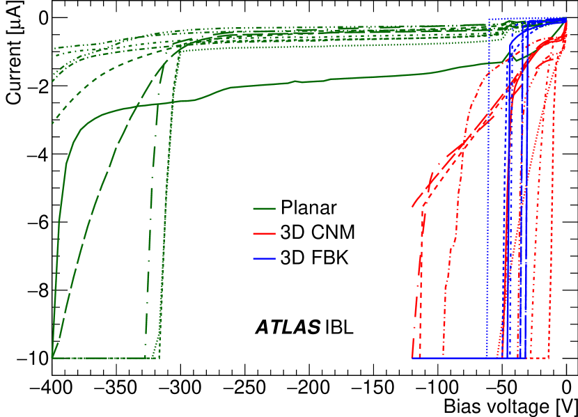
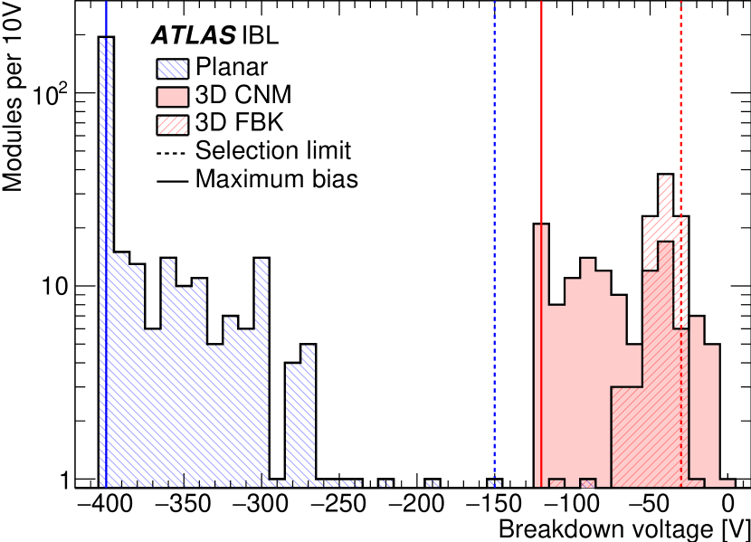
As shown in Figure 14(b), V depends on the module type. The V of planar modules was required to be less than , below the nominal bias voltage, V = . Only four of the dressed planar modules failed the sensor breakdown voltage criterion. The V of the FBK and CNM modules is , and for this reason all 3D modules having a V above at the final performance test were rejected. As already noted (Section 3.1.3), the sensor test procedure at wafer level was significantly different for the CNM and the FBK modules. For the 3D FBK modules, only one module was rejected. However, for CNM modules, the correlation between V at wafer level and for dressed modules was poor. For this reason, the wafer-level criteria were relaxed and 27 of the dressed CNM modules failed the V requirement. Furthermore, in some cases, the early soft breakdown is thought to originate in the p-stop region around the n-columns. After radiation, the leakage current due to radiation damage in the silicon bulk dominates.
3.4.2 Module time-walk and threshold tuning
During detector operation, the IBL modules digitise the measured hits with respect to the master clock, which is synchronised to the LHC clock. Only hits that are recorded within one clock cycle, i.e. within a sensitive time of , can be assigned to the correct bunch crossing of the LHC. The in-time hit detection probability is significantly influenced by the time-walk effect of the charge sensitive amplifier. Small signal charges at the input of the amplifier cross the discriminator threshold with some time delay with respect to a large reference charge and therefore the knowledge of this time-walk is important for the IBL operation.
To measure the time-walk, the time difference between the arrival time of the signal charge at the input of the amplifier and the time at which the amplifier output voltage crosses the discriminator threshold needs to be determined. During this measurement, the charge is generated by the on-chip charge injection circuitry and thus the signal charge arrival time is determined by the charge injection time, which needs to be precisely measured and adjusted. The FE-I4B chip has adjustable on-chip chip-level injection delay circuitry that is used to tune the charge injection timing. The circuitry delays the injection timing globally with respect to the chip master clock, thus decreasing the time difference between the charge injection and the digitisation time window. The injection delay is scanned and the hit detection probability is measured as a function of the delay setting for a large injected charge, using a single clock cycle digitisation window. This results in a box-shaped function as shown in Figure 15(a) for a single pixel, in this case for an injected charge of approximately . The time difference between the master clock and the charge injection (i.e. injection delay) for a hit detection probability is defined to be the hit detection time. The difference between the hit detection time for two consecutive digitisation windows is known to be (one bunch crossing) and this is used to calibrate the step-width of the delay circuitry. The step-width of this particular FE-I4B chip is . The mean hit detection time of the full pixel array is measured and the time t is defined to be the mean hit detection time of the chip plus a safety margin of to ensure that early pixel timings are not excluded.
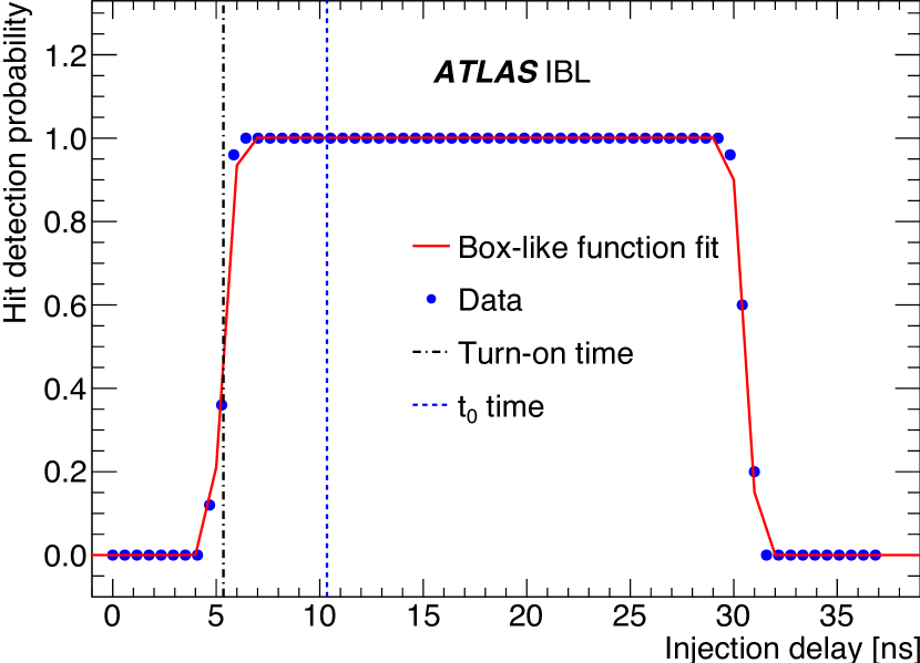
The calibration of the internal injection timing was verified with reasonable agreement using charge pulses induced in a planar sensor using a picosecond laser. The scanning procedure measuring t is similar to that based on internal injection but with the injection time being controlled outside the FE-I4B chip, thus providing an important cross check.
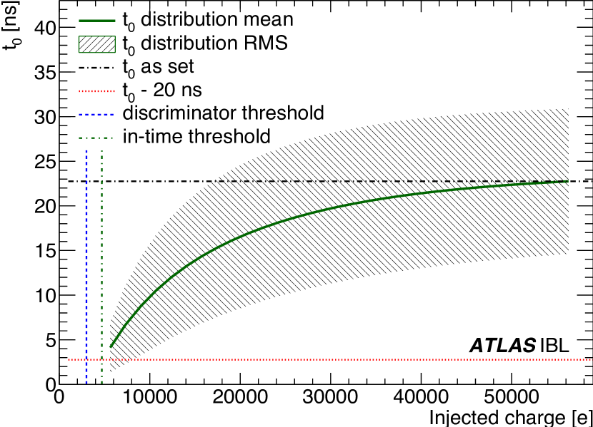
As shown in Figure 15(b) the value of t measured as a function of the injected charge reveals the effect of time-walk. For high charges the mean t saturates at a fixed delay. For small charges, closer to the discriminator threshold, t is smaller, i.e. the time between charge injection and the digitisation time window is larger. Given the safety margin added for early signals, the time-walk must not exceed for an injected charge to be detected in the correct digitisation window, i.e. the correct bunch crossing. The time-walk can be related to the input charge in electrons using Figure 15. The charge corresponding to time-walk is called the overdrive, and the in-time threshold is the sum of threshold plus overdrive. Injected charges greater than the in-time threshold will be detected in the correct bunch crossing. Smaller hits will be ’out-of-time’. Out-of-time hits can be recovered with on-chip processing. In the FE-I3 chips of the Pixel detector, there is a function to duplicate all hits below a programmable ToT value to the prior bunch crossing, at the cost of a significantly increased data volume. The FE-I4B chip contains a more sophisticated recovery method that limits the impact on the data volume. Hits with a ToT value of 1 or 2 (optional and programmable) can be replicated in the previous bunch crossing assignment, if they are adjacent to a larger hit. This exploits the fact that low-charge hits are mostly due to charge sharing, since charged particles are unlikely to produce very low-charge single-pixel clusters.
The tuning algorithm used to generate the initial module configurations included a global threshold adjustment, a module feedback current and threshold tuning, and a final iterative pixel-level feedback current and threshold tuning. The threshold was measured using a known injected charge and measuring the hit efficiency, initially at the global level and then at the pixel level. The mean value for each FE-I4B chip was tuned to be at a nominal temperature of .
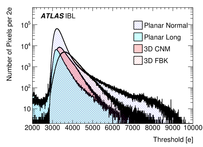
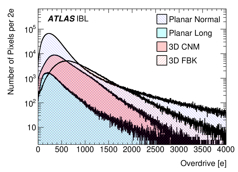
The in-time threshold can also be measured using a threshold scan algorithm with a single bunch crossing read-out, following a t adjustment. Therefore, the time-walk could be measured during the IBL module production using the so-called overdrive measurement (calculated for each pixel as the difference of in-time threshold and the discriminator threshold). Both the in-time threshold and the overdrive distributions are shown in Figure 16. The in-time threshold distributions show the expected dependence on the sensor type; the detector capacitance influences the rise-time of the amplifier and thus the mean time-walk. Similar to the noise distributions for the three module types, the overdrive distribution for planar modules (mean , RMS ) has a lower mean than for CNM modules (mean , RMS ) and FBK modules (mean , RMS ). A small number of pixel channels in the tails of the in-time threshold distribution result from poorly determined threshold fits. These mean time-walk values are well within the out-of-time hit recovery capability of approximately for the FE-I4B chip [34].
3.4.3 Module ToT-to-charge calibration
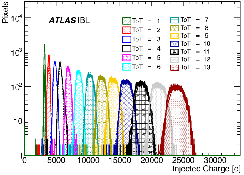
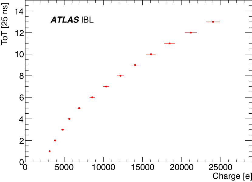
The ToT is calibrated after the discriminator threshold calibration, as that affects the ToT along with the feedback amplifier current, and vice versa. The limited available charge information due to only four ToT bits complicates the ToT-to-charge calibration. A calibration method was implemented to measure the injected charge histograms for a specific value of the ToT. For each pixel the injected charge value is stored for the pixel that responds with the chosen ToT. This results in charge histograms as shown in Figure 17(a). The mean values and the widths of the distributions of injected charge are used as a look-up table for the charge-to-ToT calibration function (Figure 17(b)). The measurement was made on each IBL module, initially for a given chip and then at the pixel level, and the result was stored for each pixel. Because of the maximum injected charge, the ToT 14 distributions were biased, and excluded from the calibration.
3.4.4 Module electronic noise
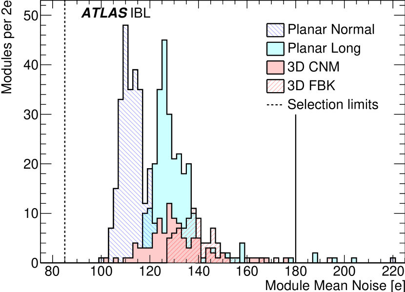
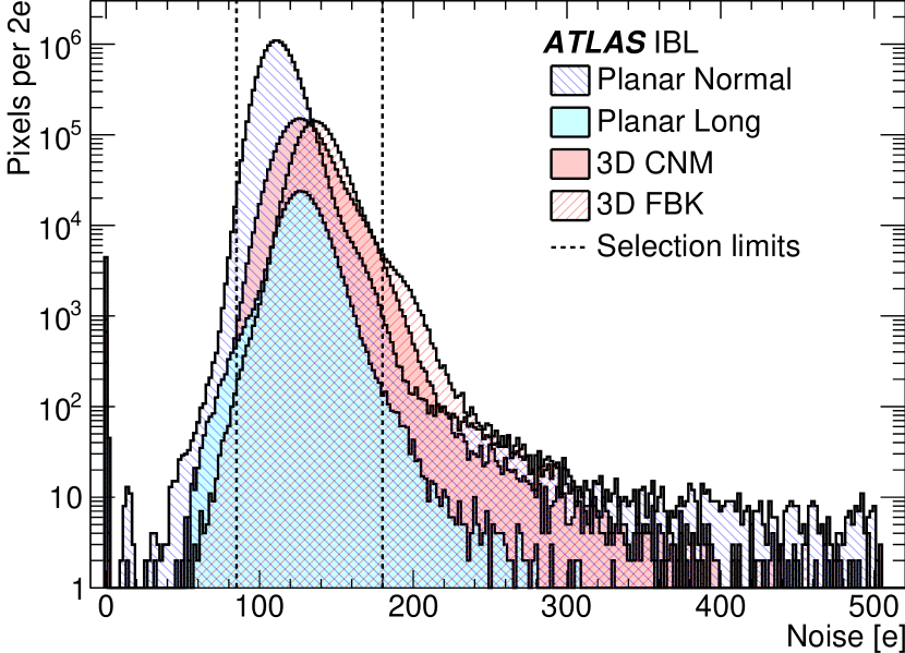
The average noise of a single pixel is measured in units of Equivalent Noise Charge (ENC)191919Noise is usually measured in charge units and is defined as the charge necessary at the input of an amplifier to generate the same output signal as the observed noise. This quantity is called Equivalent Noise Charge (ENC).. The pixel noise is an important figure of merit for the pixel module performance. It is mainly determined by the capacitance at the input node of the preamplifier and by the leakage current. Both depend on the sensor type. In addition, the noise (ENC) can be affected by external parameters such as the module flex hybrid circuit quality and the power supply stability. No influence of the IBL powering mode using the on-chip regulators is expected [37]. The noise (ENC) is evaluated from measurements of the pixel occupancy as a function of injected charge in the vicinity of the threshold value (the so-called S-curve method), using the same injected charge circuitry as that used for the pixel ToT calibration and threshold tuning. Figure 18(a) shows the mean noise (ENC) measured for each module during the full electrical test. The minimum and maximum selection limits for the mean module noise are shown by vertical lines. Figure 18(b) shows the noise (ENC) measured for individual pixels. The minimum and maximum selection limits for the noise of individual pixels are shown by vertical lines. Only of the pixels fail this selection and are flagged. The 3D modules have a higher noise (respectively and for FBK and CNM modules) in the same tuning condition as the planar modules (). This is expected because of the higher pixel capacitance of 3D sensors. The RMS width of all three distributions is comparable and ranges from to .
3.4.5 Module bump-bond connectivity and individual pixel failures
Scans to reveal possible bump failures were made at the level of individual pixels. These scans included threshold and noise measurements without the sensor bias applied, crosstalk measurements and 241Am source measurements.
As noted in Section 3.5, the initial production batches suffered from a very high bump-bonding failure rate, as determined during threshold and noise measurements at the initial test phase. Production was halted until the problem was solved.
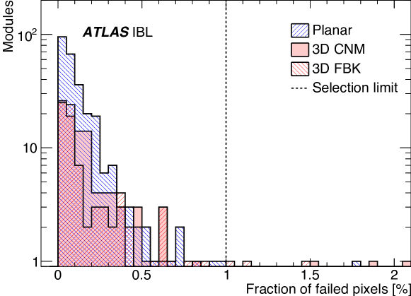
An 241Am source scan was made on each IBL module in the final test sequence and proved to be the most reliable test for open bump-bond detection. Based on the individual pixel hit rate with respect to the average hit rate per pixel for each module type, noisy pixels could be identified. Remaining bump-bonding failures could also be identified as resulting from shorts (or high electronic coupling) or open bumps. Figure 19 shows the fraction of failed pixels for each module in the final source test. Pixels with less than or more than of the mean pixel occupancy were considered as failing. A total of 19 modules had more than of bad pixels and were rejected.
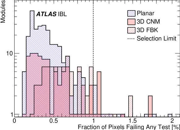
After each test of an individual failure mode, failing pixels were counted (with no double counting for multiple failures). The fraction of pixels that failed in any test is shown in Figure 20 for all modules. This fraction was required to be less than during the module production QA and was used as a basis for the final module selection. The mean fraction of failing pixels for accepted planar modules was . The mean fraction of failing pixels for CNM () and FBK () modules is comparable to the planar module distribution.
Occupancy distributions, measured using a 90Sr source after the loading of modules onto staves, are shown for each sensor type in Section 5.2.5.
3.5 Module production and yield
The IBL module production was started in July 2012 and completed in April 2014. Bare modules were delivered in batches of about twenty modules for each module type. Fully dressed modules were then assembled, tested in detail and selected according to the quality criteria described in Section 3.4. Accepted modules were then sent to be loaded on staves as described in Section 5.
After the production of the first module batches, a high bump-bonding failure rate was observed and the module production was halted for approximately four months until the problem was understood and improved procedures were implemented. Two types of bump defects were identified: large areas of disconnected bumps and a small number of isolated bumps electrically shorted to a neighbour. During the production stop, both bump-bonding defects were investigated in detail in close collaboration with the bonding vendor. Both problems were traced to the usage of a flux during the soldering process: the disassembled sensors and FE-I4B chips of defective modules showed polymerised flux residuals that acted as a spacer during the reflow, preventing a proper bump connection between the sensor and the FE-I4B pixel. For shorted pixels the results were less conclusive but flux residuals in areas with larger number of shorts were also found. The solder flux applied to the FE-I4B chip prior to the flip-chip and reflow was replaced by glycerin as the new tacking media. With this new flip-chip method neither problem recurred.
Figure 21 summarises the IBL module production yield including the first batches where the bump-bonding problems were identified. In the figure the yield is expressed in terms of rejected modules, separately for planar, CNM and FBK modules. The yield is divided into different production batches (L1 to L5) with similar laser de-bonding and flip-chip methods applied. All modules assembled with the initial flip-chip method using solder flux are grouped in L1.
Another change during the module assembly concerned the laser de-bonding of the glass carrier. The initial vendor was replaced by a second vendor, which was qualified during the production; the first modules from this vendor are in batch L3 for the planar modules, and L4 for the FBK and CNM modules.
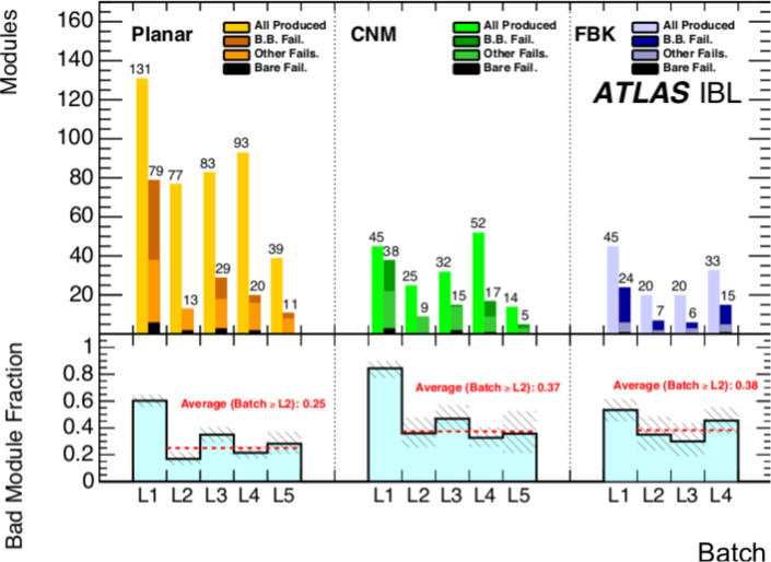
The production yield of the first batch L1 was poor for all module types because of the bump-bonding problems. Respectively , and passed the acceptance criteria for planar, CNM and FBK modules. For batches L2-L5, the yield improved to an average of , and , respectively. The initial modules coming from the second laser de-bonding vendor showed a higher rate of bump-bonding defects, mainly due to problems with the handling of the thin modules during and after the glass carrier removal. The bump-bonding failures result mainly from mis-handling during the laser de-bonding, and not on the sensor type. The mean failure rate was less than for planar and CNM modules, and for FBK modules. A summary of the failure rates, separately for the batches Lnd L L is reported in Table 8.
| Planar | 3D CNM | 3D FBK | |
| Batch L | |||
| Delivered bare modules | 131 | 45 | 45 |
| Bare module failures | 6 | 3 | 1 |
| Delivered dressed modules | 125 | 42 | 44 |
| Accepted modules | 52 | 7 | 21 |
| Bare module failures [%] | 5 | 7 | 2 |
| Bump-bonding (B.B.) failures [%] | 31 | 36 | 40 |
| Other failures [%] | 24 | 42 | 11 |
| Total failure rate [%] | 60 | 84 | 53 |
| Batches L L | |||
| Delivered bare modules | 292 | 123 | 73 |
| Bare module failures | 7 | 3 | 1 |
| Delivered dressed modules | 285 | 120 | 72 |
| Accepted modules | 219 | 77 | 45 |
| Bare module failures [%] | 2 | 2 | 1 |
| Bump-bonding (B.B.) failures [%] | 6 | 9 | 25 |
| Other failures [%] | 16 | 26 | 12 |
| Total failure rate [%] | 25 | 37 | 38 |
Other defects observed during the module production were mainly of mechanical or electrical nature. During the production a constant electrical failure rate of approximately was observed, mainly from the on-chip regulators, which were not tested during wafer probing of the FE-I4B wafers. Other electrical problems included failing double columns of the FE-I4B chip, and communications issues, but the rates were low. Several CNM modules in L2 and L3 showed problems with a low sensor breakdown voltage, due to insufficient testing procedures during the sensor wafer QA (Section 3.1.3). CNM sensors used for the batches L4 and L5 were re-tested after UBM deposition and dicing and the yield improved slightly. However, this re-testing introduced new defects on the sensors’ pixel side, increasing the bump-bonding failure rate.
The quality of each accepted module was characterised on the basis of:
-
-
The number of bad channels, based on source scan results, digital tests and other analog measurements at the operating temperature;
-
-
Electrical measurements such as the mean noise, threshold, noise dispersion, and the regulator voltages;
-
-
Mechanical anomalies or damage including non-conformal glue distribution, invisible alignment marks and reworked wire bonds.
The highest quality modules were placed closest to the interaction region.
4 Stave components
The IBL modules are supported and cooled by 14 staves, cylindrically arranged around the beam pipe axis, as described in Section 2.1. Two symmetric multi-layer flexible circuits, the stave flexes, are glued on the back of the mechanical stave structure and route electrical services between individual modules and the EoS region. The design, production and QA of the bare staves and stave flex components, and their assembly until the loading of modules on the stave, are described.
4.1 The bare stave
The bare stave should satisfy several important design criteria: a low material budget to improve physics performance; an excellent module thermal performance to optimise the pixel signal-to-noise and to prevent thermal runaway; good mechanical stability for efficient tracking performance; and a low Coefficient of Thermal Expansion (CTE) of component materials to reduce the mechanical stress.
4.1.1 Bare stave material
The constraints of low material budget and high structural reliability for the bare stave has resulted in specific design and material choices. The stave is assembled from four main components (Figures 22 and 23), together with thermally conducting epoxy202020Stycast 2850FT thermally conducting epoxy encapsulant, see http://www.henkel-adhesives.com/electronics.htm: a external diameter titanium T40 cooling tube; a carbon foam section212121K9 Carbon Foam, Allcomp Inc., see http://www.allcomp.net to drain the heat flux; carbon fibre laminates222222RS-3/K13C2U uni-directional prepress, Tencate Advanced Composites, see https://www.tencate.com to reinforce the stave stiffness; and PEEK232323Polyether-ether-ketone, VIRTEX® PEEK 450CA40, Victrex plc., see https://www.victrex.com/en/ elements to fix the stave on the IBL support.
Each of the stave components requires special manufacturing and precise machining techniques. For example, the carbon laminates require fabrication in an autoclave to obtain the required transverse thermal conductivity (). Because of the high critical pressure ( at ) of the bi-phase CO2 cooling system, the titanium cooling pipes must fulfill stringent pressure requirements, with a minimal wall thickness. The total material budget of the bare stave is . The contribution of each component is detailed in Table 9 and the main properties of the materials used are summarised in Table 10. Each stave has a length of , measured between the end block fixation points, and a width of .
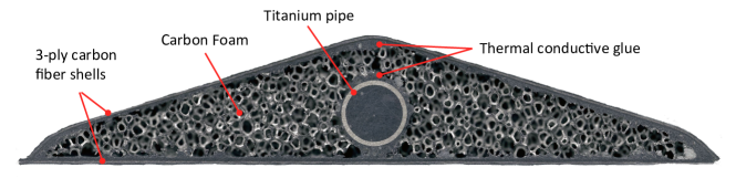
| Component | Material | Volume/stave | Equiv. Thickness | X0 | X/X0 |
|---|---|---|---|---|---|
| () | () | () | () | ||
| Back stiffener | RS-3/K13C2U prepreg | 2.020 | 0.144 | 21.1 | 0.068 |
| Epoxy layers | Stycast 2850FT | 3.290 | 0.234 | 8.97 | 0.261 |
| Carbon foam | K9 | 21.600 | 1.536 | 213 | 0.072 |
| Cooling pipe | Titanium T40 | 0.411 | 0.029 | 3.56 | 0.082 |
| Face plate | RS-3/K13C2U prepreg | 1.903 | 0.135 | 21.1 | 0.064 |
| End-of-Stave fixation | PEEK 450CA40 | 2.510 | 0.178 | 25 | 0.071 |
| Central fixation | PEEK 450CA40 | 0.075 | 0.005 | 25 | 0.002 |
| Total: | 0.621 |
| Component | Density | Thermal | CTE@ | Young’s | Tensile | Compressive |
| () | Conductivity () | () | modulus | Strength | Strength | |
| () | () | () | () | |||
| Titanium T40 | 4.51 | 16.4 | 8.6 | 102 | 430 | 340 |
| K9 carbon foam | 0.20 | 28.3 | 0.293 | 3.6 | 1.8 | |
| RS-3/K13C2U prepreg | 1.73 | (x) 96 | (x) -0.7 | (x) 410 | ||
| (y/z) 0.5 | (y/z) 15 | (y/z) 5.6 |
4.1.2 Bare stave quality control and production
The bare stave production is a 13-step process that requires careful QA to ensure a uniform quality. The QA included a visual inspection to check for cracks or mechanical non-conformities, a weight and metrology control, and a pressure test and helium leak test for the cooling tubes. A total of 33 bare staves were produced, and a similar number of prototypes were built to verify the design performance and to tune the production process. Table 11 summarises the yield of the bare stave production.
| Bare stave characterisation | Quantity |
|---|---|
| Bare staves produced | 33 |
| Staves used as prototypes | 2 |
| Staves rejected after visual inspection | 7 |
| Staves rejected after metrology | 0 |
| Staves rejected after high pressure and He leak test | 0 |
| Staves accepted for stave flex assembly | 24 |
| Bare stave failure rate during QA |
The stave weight was systematically checked to control the manufacturing uniformity. The average stave weight of the 33 produced staves is .
Given the very tight envelope requirements of the IBL, the bare stave planarity, R, is an important factor that was controlled during the metrological survey. Deviations from planarity impact the module loading activity and the minimum gap between two adjacent staves around the beam pipe. The design specification required R to be less than along the stave length. Figure 24 shows the mean planarity on all produced staves, measured at 34 points along the stave profile and in three azimuthal positions as indicated in the stave profile shown in the figure ( and at the stave edges, and at the centre of the stave). The staves have a slight undulated profile.
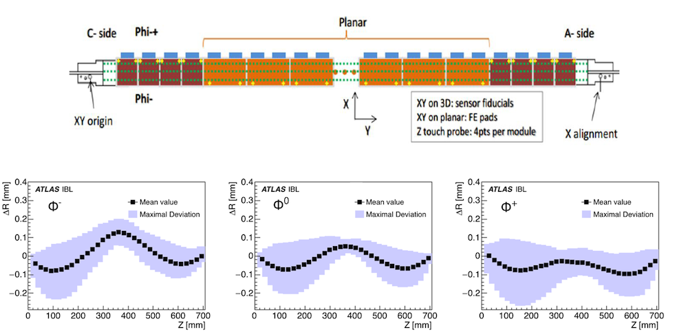
4.2 Stave flex
The on-stave electrical service lines (the stave flex) connect each module of a stave to the Type 1 internal services at the EoS. The stave flex design presented unique mechanical and electrical challenges including:
-
-
Space limitations force the services to be tightly integrated with the stave itself, with a design specification for the maximum amount of material averaged over the stave width;
-
-
High-quality transmission of data is required along the stave to the EoS, and subsequently from the EoS to the optical module (opto-board) at PP1;
-
-
The operability of the FE-I4B over the full range of drawn currents requires that the round-trip low-voltage drop is less than ;
-
-
Via interconnections are required between the Al and Cu layers.
4.2.1 Stave flex layout
A single stave is served by two stave flexes, one from each side (A and C, see Figure 3) and symmetric about the stave centre. The stave flexes run along the back-side of the stave, facing away from the interaction point. Each stave flex serves 16 FE-I4B chips and includes:
-
-
4 low-voltage (LV) supply lines, each serving 4 FE-I4B chips in parallel;
-
-
4 high-voltage (HV) supply lines, each serving either 2 double-chip planar or 4 single-chip 3D modules;
-
-
16 pairs of LVDS output lines;
-
-
8 pairs of LVDS data input and clock lines, each connected to 2 FE-I4B chips in parallel;
-
-
8 lines reading out 4 equidistant NTC (Negative Temperature Coefficient) sensors located on the module flexes242424All 3D (planar) modules carry one (two) NTC sensors mounted on the module flex hybrid. However, only four of the 16 NTC sensors are read out, to reduce the number of lines on the stave flex..
The stave flex, shown in Figure 25, consists of a longitudinal section, a dog-leg part and a connector region, with a total length of . The longitudinal section, approximately long and wide, is equipped with 16 identical wings that provide electrical and mechanical connections to the FE-I4B chips. The wing pitch of corresponds to the inter-distance between FE-I4B chips in the planar modules, but is approximately too short for 3D modules; this mis-alignment is corrected using angled wire-bonding between the wing flex and the module flex (Section 3.3.2). Each wing is long and wide. Two ears at the edge of the wing ease the gluiing of the wing flex to the module during the integration phase. As the wing needs to be bent by to be glued on the module, a row of small holes are drilled between the metallic lines to make the polyimide (Kapton®) more flexible. The dog-leg region creates a shift in both the radial and azimuthal directions, allowing services to be positioned in the correct location between cooling pipes in the EoS region. The connector region at the end of the stave is equipped with eight Panasonic AXT540124252525Narrow pitch 40-pin connectors AXT540124 (socket) / AXT640124 (header) from Panasonic Electrical Works, https://www.panasonic-electric-works.com SMD sockets.


The stave flex has six metal layers of which two are thick Al traces used for the power and ground, and four have Cu traces; the stack-up is shown in Figures 26 and 27. The total thickness is approximately . Routing between layers is achieved using vias, which are described in Section 4.2.2. Thin stiffeners are glued on the bottom under the connectors to ensure good connector insertion and removal reliability. The top metal layer is only used to route the HV signals, in order to maintain sufficient distance between the HV traces to guarantee isolation. The signal and NTC lines are distributed on the LVDS1 and LVDS2 layers, but the layout differs for the A- and C-sides to ensure the same layout for the signal connectors at the EoS. The routing of LVDS traces has been optimized to avoid cross-talk and to have a controlled differential impedance of . To better control the impedance of the signal traces on the LVDS2 layer, a Cu ground shield is added below it. This thick ground shield has a meshed structure optimised to maintain good electrical performance while minimising the additional material budget. The stave flex thickness averaged over its length and width is approximately with contributions from Al, Cu, polyimide and epoxy glue. The Cu contribution increases along the stave towards the EoS while the Al is almost constant along the stave length. The quoted material does not include the average wing contribution. The contribution of the stave flex and the wings to the IBL material budget is approximately , once smeared over the azimuthal angle. Details of the material contribution of the stave flex and wings are reported in Table 12.
| Component | Material | Thickness | Equiv. Thickness | Average X/X0 | Central X/X0 | Smeared X/X0 |
|---|---|---|---|---|---|---|
| () | () | () | () | () | ||
| Stave Flex | Cu | 61 | 7 | 0.041 | 0.011 | 0.029 |
| Al | 100 | 92 | 0.104 | 0.101 | 0.072 | |
| Polyimide | 163 | 163 | 0.057 | 0.057 | 0.040 | |
| Glue | 173 | 173 | 0.060 | 0.060 | 0.042 | |
| Total Stave Flex | 497 | 0.262 | 0.230 | 0.182 | ||
| Wings | Cu | 19 | 3.8 | 0.024 | 0.026 | |
| Polyimide | 38 | 21.4 | 0.007 | 0.008 | ||
| Glue | 10 | 5.6 | 0.002 | 0.002 | ||
| Total Wings | 67 | 0.034 | 0.036 |
The CTE of the stave flex is approximately , which is significantly different from the almost zero value of the carbon stave structure. To ensure the mechanical integrity of assembled and loaded staves during thermal cycling, the stave flex is glued to the carbon structure (Section 4.3.1).
4.2.2 The process flow
The stave flexes were produced at the CERN PCB workshop. The Cu and Al stacks (Figure 26) were processed separately. The material used for the four Cu layers were two double-sided Cu-clad laminates on polyimide substrates, one used for the TOP/LVDS2 and the other for the GND/LVDS1 routing layers. The Cu and Al stacks are then laminated together.
A feature of the stave flex is the use of low-resistivity vias joining the GND/VCC Al layers to the TOP Cu layer. Following successive etching and deposition steps to create the Al/Cu vias, there is a deposition of of Cr and of Cu in the location of the power vias. The stave flex process is completed by:
-
-
pressing together the Cu and aluminum stacks and drilling the power vias;
-
-
Cu electroplating of the power vias to connect the TOP layer with GND/VCC, followed by polyimide cover layers on the two stave flex sides;
-
-
gold plating the bonding and soldering pads and cutting the stave flex to its final shape.
The power and signal vias are shown in the cross-sectional view of the stave flex in Figure 27. The final power vias have a typical resistance of 3-.
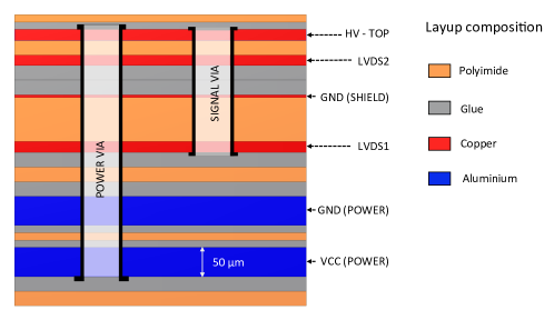
4.2.3 Quality control and production
The stave flex production was organised in batches of up to 4 sheets with three stave flexes each, all of the same type, either for the A-side or the C-side. After being diced and mounted with connectors, the flexes were cleaned and shipped to the qualification laboratory. The qualification consisted of:
-
-
a visual inspection to identify mechanical damage and surface anomalies, and a first electrical test to check resistance measurements, continuity or shorts;
-
-
the bending of the 16 stave flex wings on themselves (to allow later connection to the module flexes), with Araldite 2011 gluing on the back-side, followed by mechanical measurements and an electrical continuity test for possible broken lines, at room temperature;
-
-
ten thermal cycles between and ;
-
-
an extended (one day) HV test at with a current limit at and a final electrical verification of resistance, continuity and shorts;
-
-
a final visual inspection and sign-off for delivery.
Table 13 reports the stave flex yield. Six stave flexes were rejected during production by the vendor because of electrical or mechanical non-conformity, mainly at the beginning of the production. Two stave flexes were rejected because of a high resistivity of the LV via connection to the stave flex wings. The resistivity of the LV lines determines the round-trip voltage drop and a high inter-wing resistivity indicates a possible weak via connection. The voltage drop was uniform and typically for I = 2 A in the last batches, well within the specification. Two staves were rejected because of non-conformities identified during the visual inspection, and one stave was rejected because of HV non-conformities. Finally, electrical tests were repeated at CERN before and after gluing the stave flexes on the stave. A small HV resistivity change was observed on one stave, but the stave flex was not rejected.
| Stave flexes | Number |
|---|---|
| Produced | 72 |
| Rejected during production | 6 |
| Rejected after visual inspection | 2 |
| Rejected after the electrical test | 2 |
| Rejected after the HV test | 1 |
| Rejected after the thermal cycles | 0 |
| Rejected due to mishandling | 0 |
| Accepted for loading | 61 |
| Total failure rate | 15% |
4.3 Bare stave and stave flex assembly
4.3.1 Stave flex gluing
A pair of stave flexes is directly glued on the stave back stiffener with a procedure that was developed to meet stringent mechanical and thermo-mechanical constraints, for example the constraint of the stave envelope with an assembly accuracy of in the longitudinal direction and in the transverse direction, the thermo-mechanical characteristics of the two different materials and the minimisation of the material budget. Furthermore, the flexes must meet a radiation hardness requirement of .
Following validation of the glue deposition process, radiation hardness and mechanical stiffness, Araldite 2011 glue, together with a polyimide wet etching for the stave flex surface, were chosen. Based on these tests, a Pyralux LF111 262626Pyralux® is a DuPont Corp. trademark of a polyimide (Kapton®) substrate with a laminated or cladded layer of metal/adhesive, used for flexible PCBs, see http://www.dupont.com. In particular, Pyralux® LF111 coverlay is a polyimide film coated on one side with a proprietary acrylic adhesive. bond ply was added as a flex bottom layer in order to apply the glue to a acrylic layer after surface treatment, rather than to the polyimide directly.
The above choice was validated with an ageing test using a production IBL stave glued with production stave flexes according to the final gluing procedure. Both thermal and radiation loads were applied to the assembly during the test while using a 10 MeV electron source. After approximatively and 110 thermal cycles between and , no critical damage was observed on the stave-flex glue joint [40].
4.3.2 Quality control of stave assembly components
During prototyping, one stave flex started to delaminate after several thermal cycles. A carbon clip was added to the design in order to prevent this problem. Out of 22 production assemblies built for the IBL, only one stave encountered a critical problem due to the glue mixture mistake, which led to a polymerisation failure. The remaining assembled staves underwent a QA procedure to fully qualify the assembly before module loading. A summary of the assembled staves and their usage is detailed in Table 14.
| Staves | Number |
|---|---|
| Staves accepted for stave flex assembly | 24 |
| Staves used for system test prototypes | 2 |
| Staves assembled with stave flex | 22 |
| Staves rejected after stave flex assembly | 1 |
| Staves qualified for module loading | 21 |
| Staves loaded with modules | 20 |
As a first qualification step, the staves were visually inspected and the stave flexes were electrically tested to verify that the services were not damaged during the assembly process. The staves were then thermally stressed: an initial phase at for was followed by 10 cycles of from to and finally a stabilisation phase of at [41]. A metrology survey was made before and after thermal cycling to measure deformations of the mechanical supports by the flex gluing and to verify that the assembly still respected the required envelope. The stave planarity measurements, before and after thermal cycling, are summarised in Figure 28 [41]. The planarity of one typical stave before and after flex gluing, and after thermal cycling, is shown in Figure 29. As expected, due to the different CTE of the materials and the stave flexes being glued on just one side of the back of stave, the shape of the mechanical supports is affected by the assembly of the flexes and by the thermal cycling. Before thermal cycling, only four staves exceeded the specified bare stave envelope of . After thermal cycling, the planarity is slightly deteriorated, but remains less than and within the clearance after integration in the IST of .
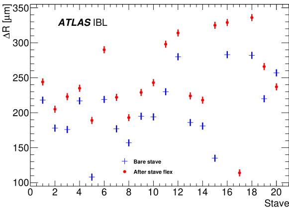
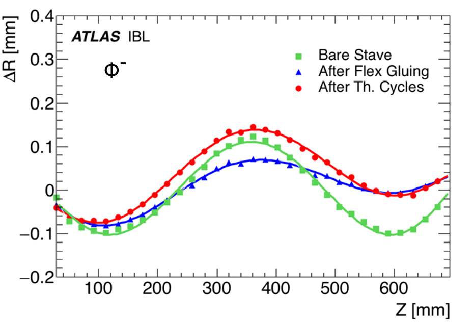
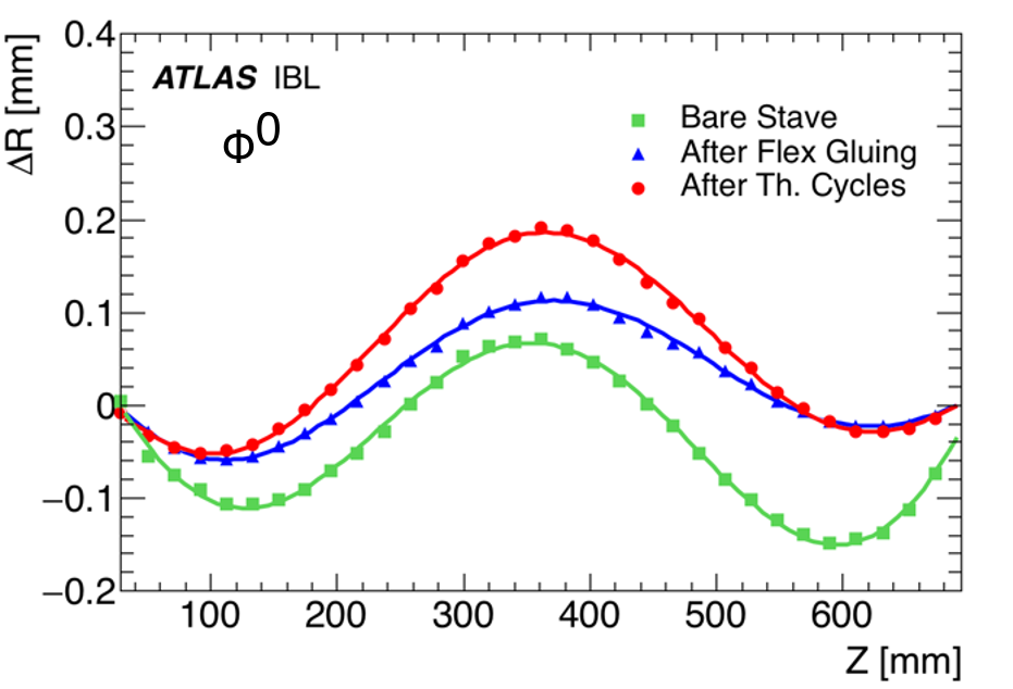
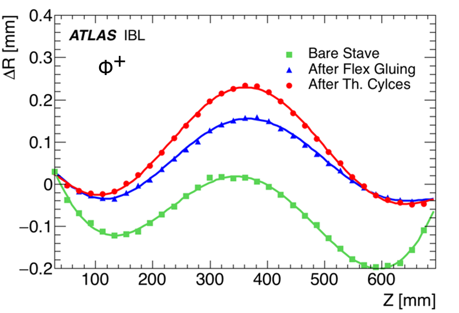
5 Stave loading and quality assurance
Twenty staves were loaded with qualified good modules. Details are provided in reference [41]. The QA procedure [42] provided a detailed characterisation of the stave including calibration in cold conditions and data taking with radioactive sources. Pixel defects were classified according to the type of failures observed in the FE-I4B chip, in the sensor and in the bump bonding. Two staves were accidentally damaged by an excess of humidity during the QA procedure (Section 5.4). Of the 18 remaining staves that satisfied the QA procedure, the best 14 were selected for assembly in the IBL detector.
5.1 Stave loading and rework
Qualified modules were loaded on the staves following the procedure described below and sketched in Figure 30. Each qualified stave was installed in a loading tool where a thick thermal grease272727HTCP, Electrolube, see https://www.electrolube.com/core/components/products/tds/044/HTCP.pdf. layer was applied to half of its surface using a stainless steel template shim. After removing the template, the positioning tools were installed, and two Araldite 2011 glue drops per FE-I4B chip were applied with a needle on the thermal grease template openings to later fix the modules on their position. The modules were then installed, one at a time, using spacers to achieve a precise gap between neighbouring modules. A load of per FE-I4B chip was placed on the modules during the glue-dot curing period. After the removal of weights and positioning tools, an optical inspection was performed before repeating the process on the other half of the stave.


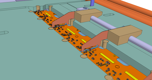
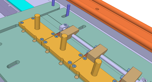
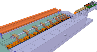
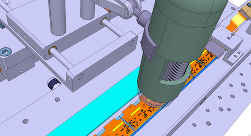
After loading, the modules were connected to the stave flex following the procedure sketched in Figure 31. First a layer of Araldite 2011 was deposited on each of the stave flex wings using a mask. A tool constrained the wings to stay in their nominal position. A load of per FE-I4B chip was applied during the glue curing period. A -thick Kapton® insulator was then inserted between each powering sector. Finally, wire-bonds were added to connect the modules to the wings of the service flex, enabling the stave powering and data transmission. As a last step, the stave envelope was checked to ensure that the mechanical constraints of the IBL were fulfilled.


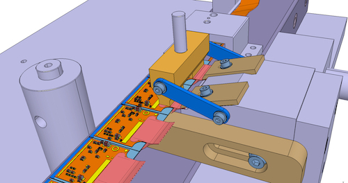


A module re-work procedure, sketched in Figure 32, was established to replace modules if required as a result of mechanical damage or functional issues. A -thick Kapton® spacer and holders were installed at each side of the module to be replaced, protecting the neighbouring modules. The module was removed using a spatula and the stave face plate was cleaned from grease or glue. A new module was then loaded following the procedure described above, using a set of dedicated tools. In total, twenty-two modules were re-worked: fifteen modules were replaced due to module damage during the module loading procedure that compromised the integrity of the sensor, the FE-I4B chip or the module flex; five modules were replaced because of failures of the FE-I4B chip after loading; and two modules were replaced because they failed the QA tests made before final integration. In addition, due to the cleaning and re-bonding intervention performed (Section 5.4), six modules were replaced on the twelve re-bonded staves.
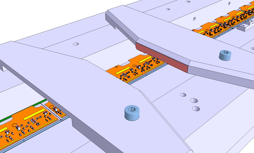


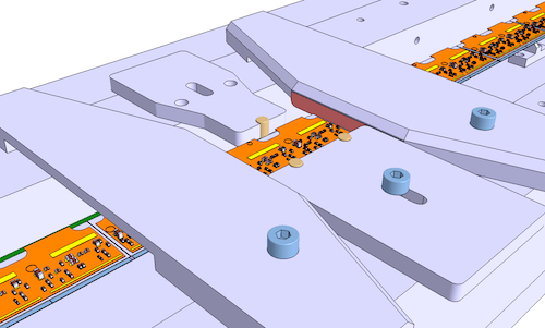

5.2 Quality assurance of the stave assemblies
5.2.1 Stave cooling performance
An essential aspect of the stave design is the removal of heat from the IBL modules, under any foreseeable environmental and running condition. The sensor temperatures must be controlled, as an increasing sensor temperature will result in an increased sensor leakage current that may lead to thermal runaway [43], damaging the module. To minimise the effects of reverse annealing and thermal runaway in the sensors, the target temperature of IBL modules during operation is below . Furthermore, the modules must remain cool during beam-pipe bake-out procedures when the beam pipe at the IBL contact points reaches .
The bi-phase CO2 cooling system (Section 7.5) was chosen to achieve the required low temperature module operation while minimising the pipe diameter and the associated radiation length [44]. The external diameter titanium T40 cooling tubes have a wall thickness to meet the CO2 critical pressure ( at ) requirements.
Several simulations were performed to estimate the stave thermal performance, quantified by the Thermal Figure of Merit (), i.e. the thermal resistance between the cooling fluid and the sensor surface. Considering the various heat sources and an active sensor area , the sensor temperature can be expressed as:
where is the power dissipated in the chip; is the power dissipated in the module flex; and is the power dissipated in the sensor. In worst-case conditions for , and , the thermal runaway was estimated to occur for the > .
Figure 33(a) shows the measurement for a prototype stave during the final design qualification. The measured
is for , conservatively a factor two below
the value at thermal runaway. To qualify the thermal performance of the stave during production, the temperature uniformity was measured for each stave after module loading. All of the installed staves show a temperature dispersion within , as shown in Figure 33(b), which is a good indication of the production uniformity.
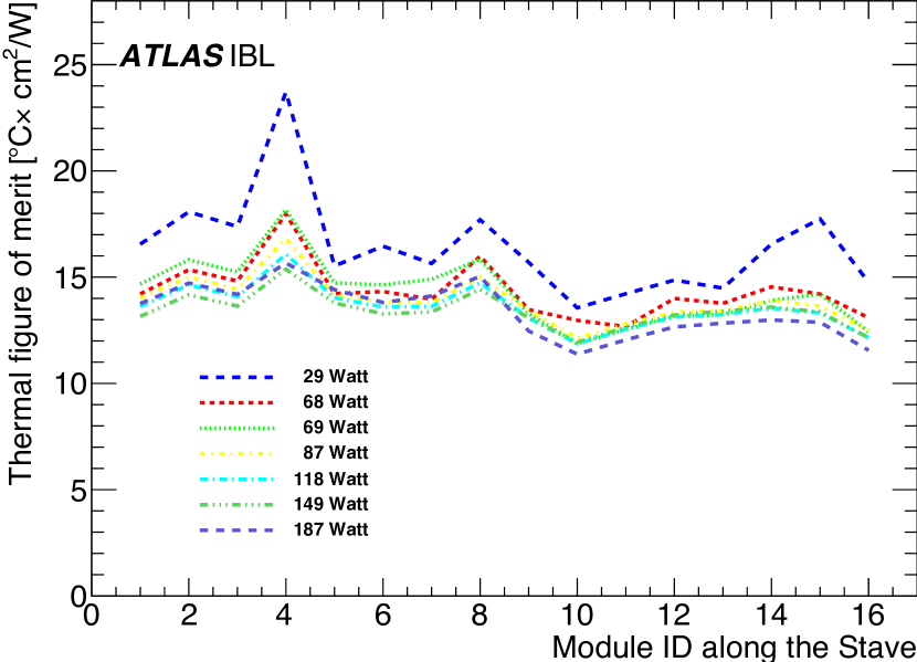
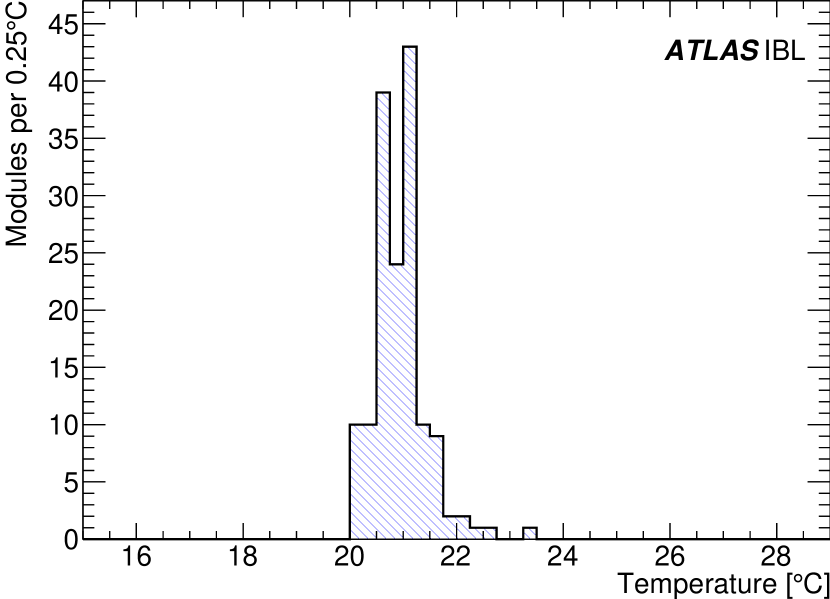
5.2.2 Metrology survey
An optical survey of the stave assemblies was made using the four fiducial marks placed on each module. The error distributions of the module loading position are shown in Figure 34 for the and axes282828For the definition of the and directions refer to Figure 24.: an RMS precision of is measured for planar modules in both directions, and for 3D modules an RMS precision of in and in is achieved.
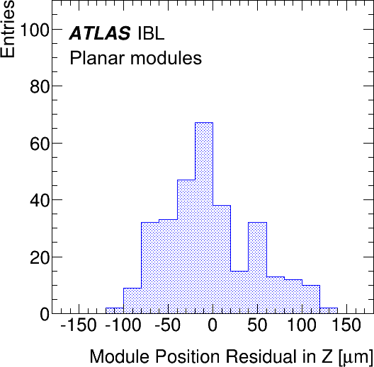
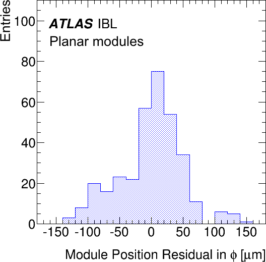
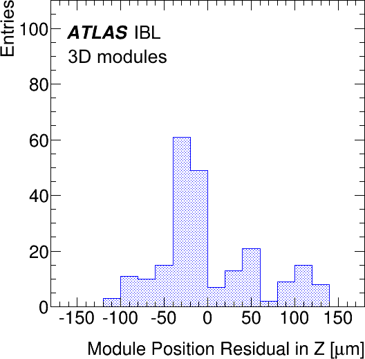
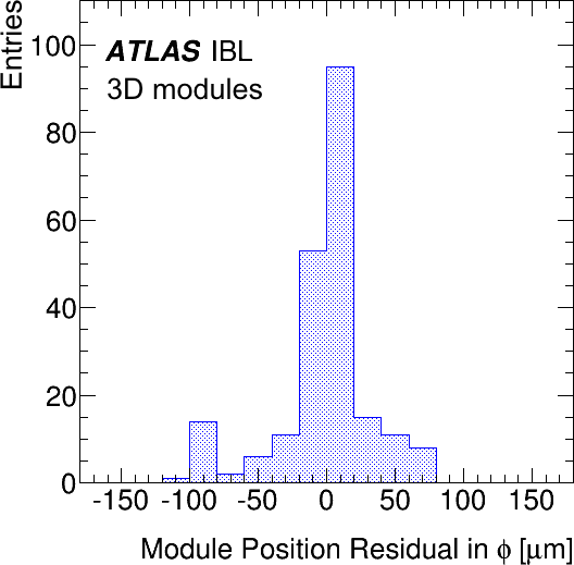
5.2.3 Functional qualification
Following the metrology survey, the staves were transported to CERN where the final stave qualification was carried out. Results from the electrical qualification [42] were an important input for the selection of the 14 staves that were integrated in the final detector.
The electrical QA test stand could operate two staves simultaneously. The staves were installed in an environmental box, which was flushed with dry air to maintain the humidity below , corresponding to a dew point of for the minimum box temperature of . The temperature on the staves was controlled by a TRACI292929 Transportable Refrigerator Apparatus for CO2 Investigation, https://ep-dep-dt.web.cern.ch/co2-coolingplants/traci-geneve. CO2 cooling plant.
The Detector Control System (DCS) and the Data Acquisition (DAQ) for the test stand emulated the DCS and DAQ of the installed IBL detector, described in Sections 6.2 and 6.3. They were connected to the stave using custom EoS PCBs. The read-out system used the Reconfigurable Cluster Elements (RCE) architecture based on ATCA technology [45]. As for the installed IBL detector, the DCS granularity was a group of four read-out chips; it was not possible to record and control individual modules. The nomenclature of the FE-I4B chips as used for the stave QA, and of the DCS read-out for a stave, are shown in Figure 35.
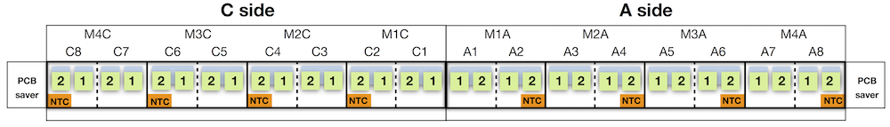
A detailed optical inspection of each stave was made before and after the QA procedure. Photographs of each chip were taken with a high resolution camera to identify any major damage to the chip, as well as debris that might have been left on the stave during assembly or wire bonding. A detailed microscope inspection of the stave was then made.
The electrical functionality of each stave was next verified, before making calibration measurements. This included power-up studies, the verification of set voltages and currents in un-configured and configured FE-I4B chip states, and I-V characteristics of the sensors. The powering behaviour of the modules was verified during ten LV power cycles. The time dependence of current and voltage from this test are shown for stave ST12 in Figure 36(a). Most modules show a stable current consumption for every cycle; current fluctuations can be explained by improperly reset chip registers. After a first successful power-up of the stave, the temperature, the set voltage reading, and the currents before and after read-out configuration of each DCS group, were recorded. The expected values during the stave QA are listed in Table 15.
| Quantity | Expected Value |
|---|---|
| Temperature | |
| Voltage | |
| Unconfigured current | |
| Configured current | |
| Leakage current | Compatible with module QA |
An I-V scan was performed to characterise the sensor quality. The sensor HV was ramped in 20 steps from 0 to for 3D sensors and from 0 to for planar sensors. The I-V characteristics of the DCS module group of four read-out chips was required to be compatible with the measurements performed on modules before the stave loading. Results for stave ST12 are shown in Figure 36(b). For this particular stave, one DCS group (M4C) indicated a 3D sensor I-V breakdown, above the operating voltage and still within the QA specification.
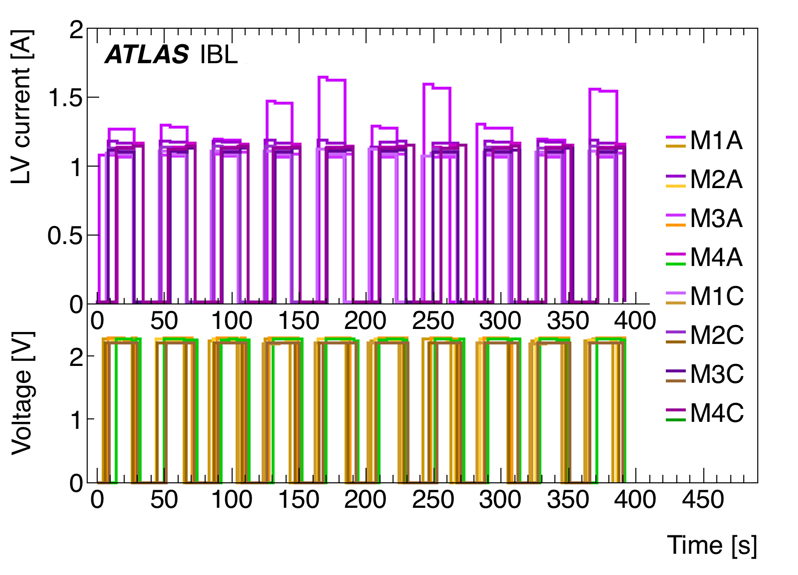
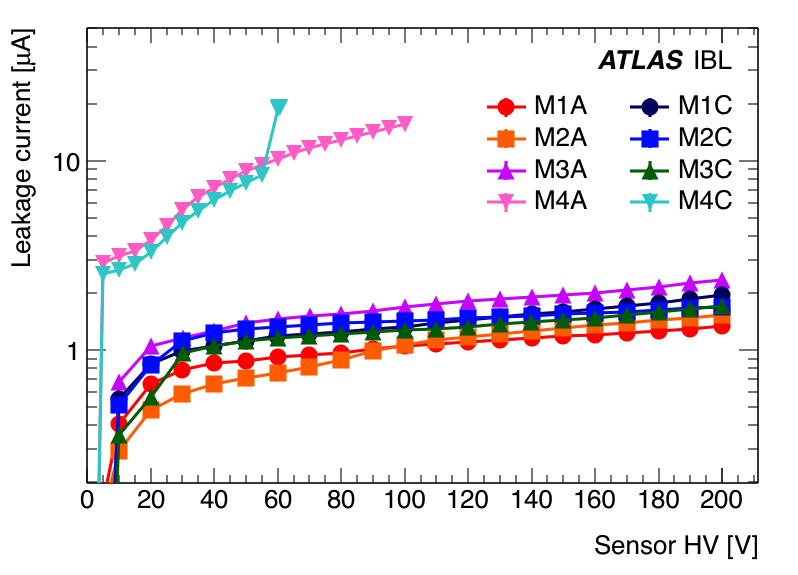
A series of basic functionality tests, including the digital functionality, the t calibration and threshold, ToT and crosstalk scans, were also made, using the module configurations recorded at previous module QA testing sites (Section 3.4). This allowed a direct comparison of the stave functionality, and discrepancies indicating possible damage induced during module loading or transportation to CERN.
A comparison of threshold scans with and without HV allows the identification of areas of disconnected bumps, since a pixel that is no longer connected to the sensor is not affected by the higher noise present when the sensor is not fully depleted. Nevertheless, a source scan is needed to fully identify all disconnected bumps as described in Section 5.2.5.
5.2.4 Stave calibration
Following a t calibration, the discriminator threshold and the ToT parameters of the FE-I4B chips must be calibrated and tuned to distinguish charged particle signals from electronic noise, and to ensure that the charge determination is uniform over all IBL pixels. The selected threshold should be as low as possible to ensure maximal detector efficiency for charged particles (especially when the charge is shared between pixels), and to ensure the best possible ToT tuning. It should also be sufficiently high to discriminate against electronic noise.
During the module QA (Section 3.4), a mean module threshold of . To compare with those results, the same calibration working point was retained. A more realistic operating condition is to use a lower pixel threshold as noted above. A second calibration working point of at an operating temperature of was chosen [42]. The mean threshold can be tuned for each FE-I4B chip using charge injection circuitry. As for the QA of individual modules, the pixel noise (ENC)303030ENC is defined in Section 3.4.4. is evaluated from a measure of the pixel occupancy as a function of injected charge, using the FE-I4B charge injection circuitry (the S-curve method).
In each case the ToT was tuned to 10 units of for a charge of , corresponding to a minimum ionising particle at normal incidence. Figure 37 shows the one-dimensional ToT distribution for all pixels when tuned to 10 ToT, and the mean ToT as a function of chip number along the stave. The data are shown for a mean module threshold of at .
The threshold calibration results for the complete set of staves are summarised in Table 16. The pixel-to-pixel RMS of the threshold distribution (threshold RMS), of approximately , is compatible with the accuracy of the injection circuit. Figure 38 shows the threshold and noise (ENC) distributions for individual pixels, in the case of a threshold tuning at . Figure 38(a) indicates that all of the modules could be tuned to a mean threshold of , with only a few individual pixels that could not be tuned to that value.

| Tuned Threshold | Pixel Type | Threshold RMS [] | ENC [] | Threshold-over-Noise |
|---|---|---|---|---|
| at | Planar Normal | 37 | ||
| Planar Long | 58 | |||
| 3D FBK | 39 | |||
| 3D CNM | 40 | |||
| at | Planar Normal | 42 | ||
| Planar Long | 47 | |||
| 3D FBK | 46 | |||
| 3D CNM | 41 |
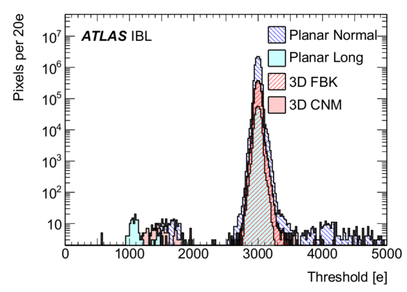
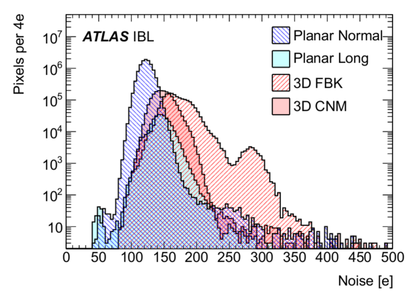
The threshold-over-noise distributions for and tunings are shown in Figure 39; this quantity is the key parameter in determining the quality of the IBL modules with respect to their operability at a given discriminator setting. The physics occupancy in the ATLAS Pixel B-Layer was approximately hits per pixel per bunch crossing unit of at the end of Run 1 and that for the IBL was expected to be approximately hits per pixel per bunch crossing unit at the beginning of its operation. Pixels with a noise occupancy rate higher than hits per pixel per bunch crossing unit were considered to be noisy and were disabled from data taking. A threshold-over-noise value larger than 5 ensured a noise contamination in IBL physics hits of less than . For the reference tuning at module temperature, the observed fraction of noisy IBL pixels was less than .
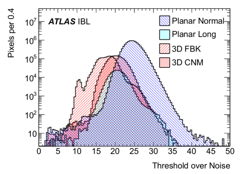
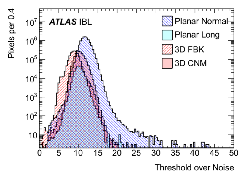
Figure 40 shows the threshold and noise distributions averaged over all 18 qualified staves as a function of chip number for the reference tuning. Figure 40(a) shows that it was possible to tune all production staves to within . The average noise was approximately for planar sensors and less than about for 3D sensors. Slightly higher noise was observed on the A-side of the setup: this was due to a combination of increased noise on the HV lines of the setup and the fact that FBK modules, which are more sensitive to external noise, represented the majority of the 3D sensors on this side.
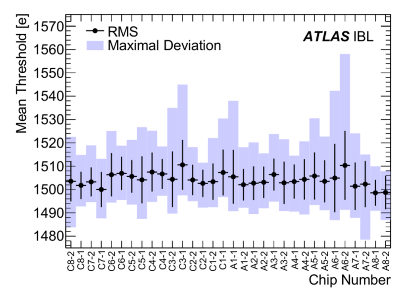
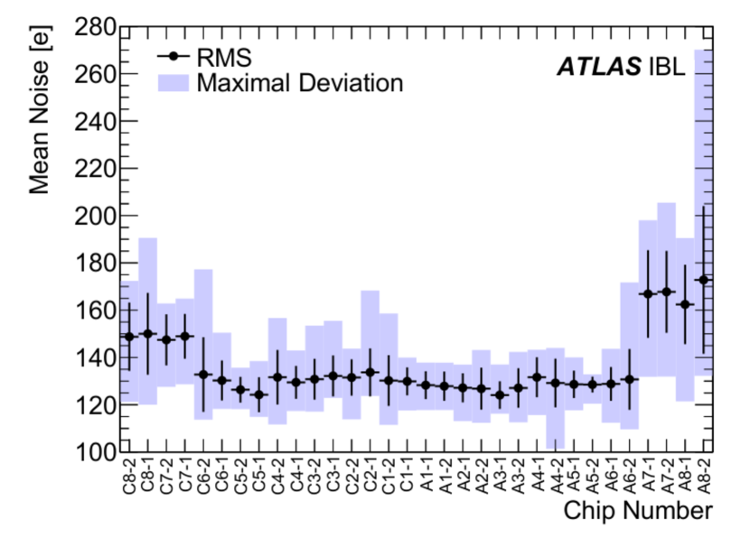
5.2.5 Source scans
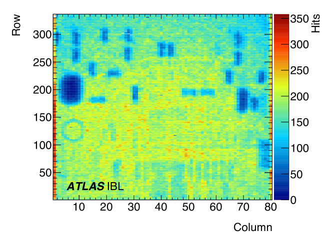
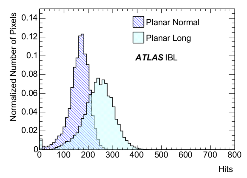
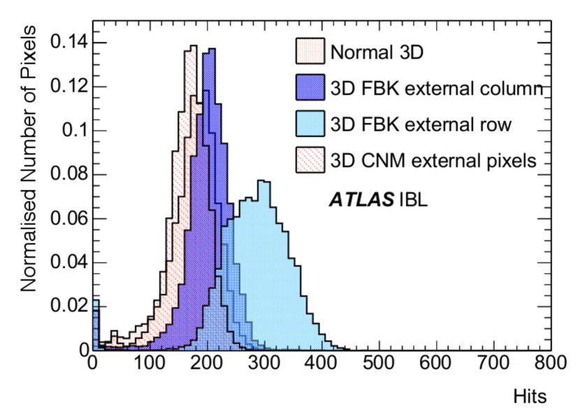
Source scans were performed with a threshold configuration using a 90Sr source and an internal self trigger mechanism. An example of a source scan hit map for a single 3D FBK module is shown in Figure 41. Regions with a lower number of hits are clearly visible and match the passive components mounted on the module flex. Each normal pixel collected approximately hits. An increased hit occupancy in the edge columns and the edge rows is due to an increased active area for FBK pixels resulting from the fence structure at the edge. Figure 42(a) shows the hit occupancy for planar pixels, separating the categories of normal pixels and long pixels. The mean hit occupancy is less than that for 3D modules because of the reduced sensor thickness ( instead of ). Figure 42(b) shows the occupancy for normal and edge pixels of CNM and FBK modules. Because of their guard-ring design CNM sensors do not show an excess in the edge rows and columns. Although not shown, CNM sensors also have a slightly lower occupancy than FBK sensors for normal pixels because of the smaller depth of their columnar electrodes.
Source scans were mainly used to identify disconnected bumps, but it was also possible to check the average charge using the 90Sr source. This used the ToT distribution of all clusters with more than one hit313131Clusters are formed by groups of hits collected by adjacent pixels.. Figure 43(a) shows the most probable value (MPV) of the Landau-Gauss fit of such distributions as a function of FE-I4B position, averaged over all staves; the MPV distribution of each chip is shown in Figure 43(b). The different behaviour between 3D and planar modules is due to their different sensor thickness. The difference with respect to the calibrated mean of 10 ToT is small.
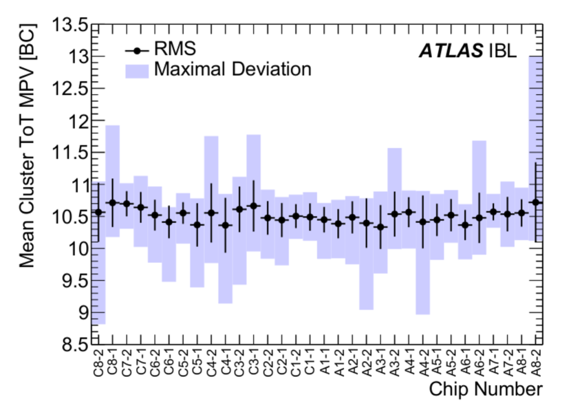
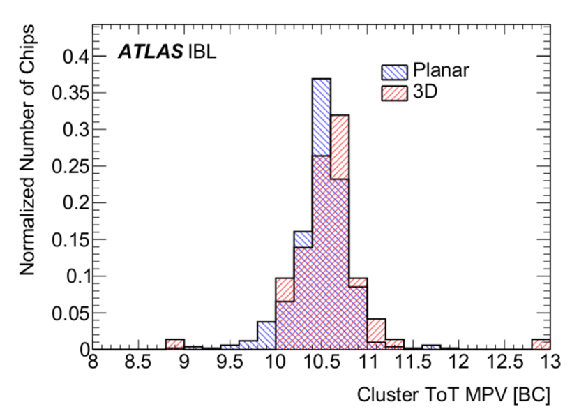
5.2.6 Pixel defects
Faulty pixels were classified on the basis of calibration and source scan results and assigned to a single category listed in Table 17. This table indicates the failure type, the method used to identify the failure, and the detailed selection criteria.
| Failure Name | Scan type | Criteria | ||
|---|---|---|---|---|
| Digital dead | Digital scan | Occupancy | of signal injections | |
| Digital bad | Digital scan | Occupancy | or of signal injections | |
| Merged bump | Analog scan | Occupancy | or of signal injections | |
| Crosstalk scan | Occupancy | of signal injections | ||
| Analog dead | Analog scan | Occupancy | of signal injections | |
| Analog bad | Analog scan | Occupancy | or of signal injections | |
| Tuning failed | Threshold scan | s-curve fit | Fit failure | |
| ToT test | ToT response | 0 or 14 ToT units of | ||
| Noisy pixel | Noise scan | Occupancy | hits per bin | |
| Disconnected bump | Source scan (90Sr) | Occupancy | of mean occupancy | |
| High crosstalk | Crosstalk scan | Occupancy | with signal injection |
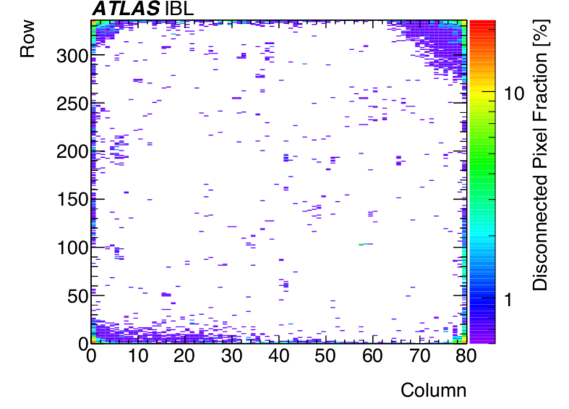
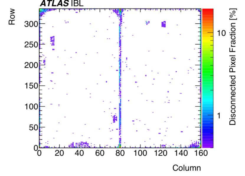
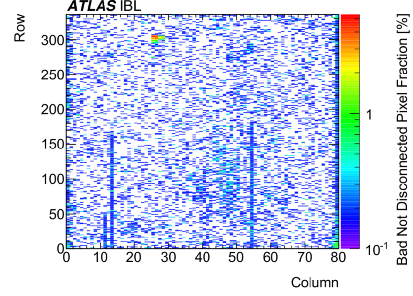
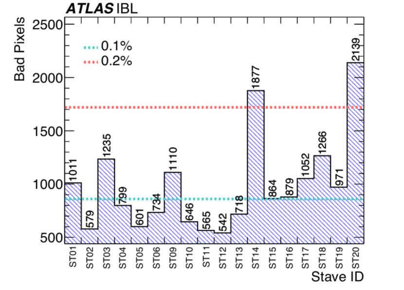
Most of the failures relied on the module showing an excess or deficit of the hit rate. The digital and analog functionalities can be directly tested with respectively digital and analog scans. Dead digital and analog pixels are common electronic failures. However, the digital and analog bad categories only appear in high numbers for the case of a low ohmic connection between pixels or the identification of a merged bump as occurred in early production batches (Section 3.4). The merged bump category exists when two solder bumps connecting the sensor to the read-out chip are merged and manifests itself in an analog failing pixel which still gives a response in a crosstalk scan. A pixel is classified as untunable if the threshold or ToT cannot be tuned at all; nevertheless a high discrepancy from the tuning target is accepted as these pixels can still be used for operation. The noise occupancy, which indicates how many hits per BC are produced due to noise, is a very important diagnostic and operational quantity. The easiest way to identify a disconnected bump is to analyse the response from a source scan. If a pixel shows zero or only very few hits in the source scan data, the bump is assumed to be disconnected (Section 3.4). The high crosstalk pixel category is not directly related to the performance of the pixel but if a sensor pixel shows significant charge sharing with a neighbour, this can influence the precision of the offline reconstruction.
The total fraction of bad pixels, averaged over all modules, is shown in Figure 44. No clear correlation was found between the chip topology (other than edge regions) and the measured disconnected bumps. There was a clear increase in the number of bad pixels towards the stave ends because of the choice to load the best modules into the central region of a stave. The number for each bad pixel category is collected for each stave in Table 18.
| Stave | Digital | Analog | Disconnected | Merged | Untunable | Noisy | High | Total |
|---|---|---|---|---|---|---|---|---|
| fault | fault | pixel | bump | pixel | crosstalk | |||
| ST01 | 6 | 389 | 272 | 3 | 232 | 11 | 98 | 1011 |
| ST02 | 10 | 255 | 54 | 3 | 117 | 15 | 125 | 579 |
| ST03 | 6 | 375 | 473 | 0 | 182 | 21 | 178 | 1235 |
| ST04 | 2 | 201 | 254 | 0 | 275 | 8 | 59 | 799 |
| ST05 | 2 | 207 | 172 | 0 | 183 | 4 | 33 | 601 |
| ST06 | 6 | 206 | 337 | 0 | 147 | 9 | 29 | 734 |
| ST09 | 8 | 360 | 476 | 3 | 167 | 8 | 88 | 1110 |
| ST10 | 16 | 179 | 304 | 0 | 141 | 3 | 3 | 646 |
| ST11 | 10 | 196 | 159 | 0 | 155 | 8 | 37 | 565 |
| ST12 | 15 | 172 | 169 | 0 | 166 | 7 | 13 | 542 |
| ST13 | 9 | 127 | 205 | 0 | 336 | 6 | 35 | 718 |
| ST14 | 4 | 161 | 1364 | 0 | 330 | 7 | 11 | 1877 |
| ST15 | 5 | 222 | 350 | 0 | 259 | 20 | 8 | 864 |
| ST16 | 1 | 237 | 414 | 1 | 187 | 15 | 24 | 879 |
| ST17 | 2 | 214 | 598 | 0 | 229 | 5 | 4 | 1052 |
| ST18 | 13 | 161 | 902 | 1 | 178 | 2 | 9 | 1266 |
| ST19 | 10 | 163 | 543 | 0 | 228 | 11 | 16 | 971 |
| ST20 | 14 | 224 | 1051 | 0 | 535 | 13 | 302 | 2139 |
A production cut of 100 bad pixels per chip was initially applied after the module assembly. This cut was relaxed at the end of the production because of a shortage of 3D sensor assemblies; of all chips loaded onto staves had less then bad pixels.
The total number of failing pixels per stave is shown in Figure 44(d). The dashed lines indicate the and marks; the specification required a stave to satisfy . All staves were well within the specification; of the staves had failing pixels and of those staves had . Approximately of all failures were due to disconnected bumps, the other were distributed between a pixel with failing analog functionality, or a bad ToT tuning.
Correlations between the defects observed at this stage and in the module production were extensively studied [42]. Although similar selections to classify a pixel were used in the two test stages, a more intense test procedure was applied during module production and more bad pixels were detected per FE-I4B chip. However, there was a good correlation between the number of bad pixels per FE-I4B chip in the two tests. Moreover it was verified that there was no significant increase of bad pixels in specific geographical areas, for example the chip edges, thus excluding damage resulting from the module transport, handling and stave loading.
5.3 Stave ranking and layout assignment
Of the 18 qualified loaded staves, 14 staves were selected for integration as part of the IBL. The stave quality was scored by a geometrical inefficiency based on a -weighted bad pixel fraction, together with an algorithm developed to minimise the clusterisation of bad pixels in . In addition, two artificial constraints were applied: the first and the last integrating staves were required to have the best planarity in order to simplify assembly; and staves that were re-worked as a result of corroded wire bonds (Section 5.4) were loaded alternately.
Table 19 summarises the position of each stave in the IBL loading map, and other characteristics of the staves considered in the selection. Figure 45(a) compares the average bad pixel fraction for the 14 installed staves with the four non-installed staves, as a function of . The average bad pixel fraction for the integrated IBL staves is for and over the full range. The corresponding fractions for the four non-installed staves are respectively and . Figure 45(b) shows the distribution of bad pixel fraction as a function of and . The stave overlap is taken into account in this figure.
| Position | Stave | Number of bad pixels | Planarity [] | Reworked because of corrosion |
| 01 | ST17 | 1052 | 114 | no |
| 02 | ST02 | 579 | 205 | yes |
| 03 | ST19 | 971 | 266 | no |
| 04 | ST09 | 1110 | 229 | yes |
| 05 | ST18 | 1266 | 336 | no |
| 06 | ST04 | 799 | 235 | yes |
| 07 | ST13 | 718 | 224 | no |
| 08 | ST10 | 646 | 243 | yes |
| 09 | ST11 | 565 | 298 | no |
| 10 | ST12 | 542 | 314 | yes |
| 11 | ST16 | 879 | 329 | no |
| 12 | ST06 | 734 | 290 | yes |
| 13 | ST15 | 864 | 325 | no |
| 14 | ST05 | 601 | 189 | yes |
| n/a | ST01 | 1011 | 224 | yes |
| n/a | ST03 | 1235 | 223 | yes |
| n/a | ST14 | 1877 | 218 | no |
| n/a | ST20 | 2139 | 237 | no |
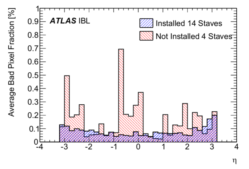
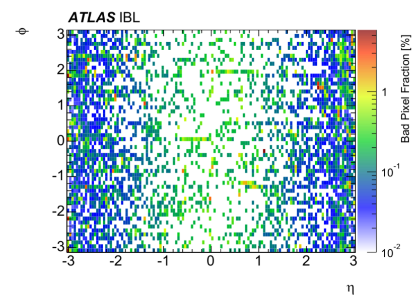
5.4 Wire bond corrosion
During the IBL production, two production staves were damaged during testing inside the QA environmental box. While the staves were in operation and cooled at , ice was identified around the coldest part of the staves. The two staves were carefully inspected under a microscope and it was discovered that most of the aluminium wire bonds were corroded (Figure 46), with a few broken. A white residue around the bond foot could be easily identified with ring lighting. The other staves were re-inspected and, of the 12 staves already produced, 11 staves were identified to suffer from bond corrosion.
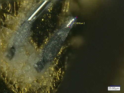
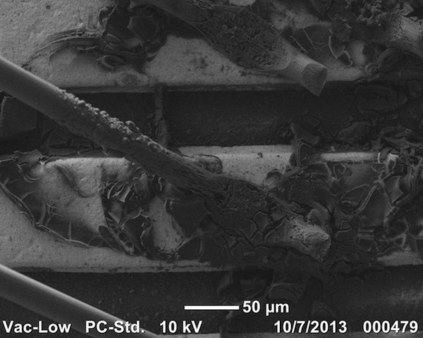
Production was halted until the problem was understood. A number of successive actions were taken:
-
-
Identify the origin of the corrosion and identify corrective actions such as to improve the QA procedure, before resuming the production;
-
-
Investigate the evolution of the corrosion and identify possible preventive actions, for example cleaning and coating;
-
-
Organise a re-work centre to clean all the wires and to re-bond the 11 defective staves;
-
-
Launch an additional module production with remaining components to ensure a sufficient number of IBL staves for the integration.
The investigation initially considered the possibility of humidity in the QA environmental boxes, and it was found that 2 setups were concerned. The first concerned the climate chamber used to qualify loaded staves by temperature cycling in the range to . As shown in Figure 47, the dew point was reached for a few minutes in the proximity of the stave modules during the fast temperature ramp-up because of local restrictions to the dry air flow, even though the volume was flushed with dry air and the chamber humidity control was activated [41]. The stave electrical and mechanical integrity was not affected by the corrosion: this was confirmed by electrical characterisations and metrology surveys. For the remainder of the production, the newly loaded staves were not thermally cycled. The second problematic environmental box was that used for the stave electrical qualification at low temperature. Upgrades to improve the stave dryness and the reliability of the environmental control were made by adding dedicated interlock actions on the cooling and the power supply.
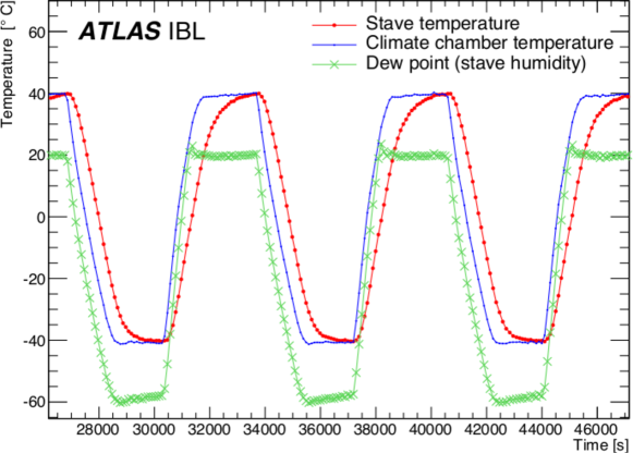
5.4.1 Investigations of the Al wire corrosion process
The interconnection of Al wires with the Ni/Au bonding pads remains an issue even at room temperature, because of the galvanic coupling between Au and Al. During the ultrasonic wire bonding the Au layer is locally removed and the final metal contact is between Al and Ni. In addition the Al wire is normally protected by a thin oxidation layer that is formed in a few hours and that stabilises at a thickness of about 5 nm. This protective layer can be damaged in the presence of water or because of mechanical or chemical attack. If this occurs, as during the stave cold test, a corrosion process will be initiated.
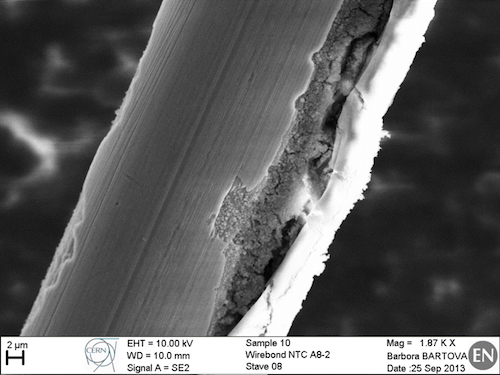

The corrosion residues and Al wires were analysed (Figure 48) with an Energy Dispersive X-Ray Spectroscopy (EDS) technique and the presence of C, O, Ca, Na, Cl, F at a level of up to a few percent was detected. The presence of ionic compounds indicated that the cleaning of the module flex after SMD assembly should be improved. The corrosion process was easily reproduced in the laboratory, even in presence of de-ionised water on wire bonded samples. However, further investigations revealed that the process was even observed on ultra-clean bare flex assemblies. Additional cleaning procedures such as plasma cleaning proved ineffective in stopping the occurrence of corrosion, although its effect could be mitigated.
A sample analysis was also performed with an X-ray Photoelectron Spectroscopy (XPS), alternating the measurements with the sputtering of the Au layer with Ar ions. This probed the atomic spectrum at the Au surface while removing subsequent layers until reaching the Ni interface. The procedure was applied to several flex circuits delivered by two different producers 323232Laboratory studies showed that the susceptibility of the flexes to corrosion was vendor dependent. In particular, the flexes used for the Pixel detector were much less sensitive to corrosion. . On one sample fluorine was detected at a significant level (up to at a depth of ). This presence could not be understood nor reproduced in other flex circuits from the same producer.
Options considered to protect against corrosion included the potting of the bond foot and the use of spray coating such as polyurethane, but neither were possible because of the tight production and integration schedule. All wire bonds showing signs of corrosion were replaced. It was decided to leave the wire bonds unprotected, but to ensure that a safe humidity level would always be maintained during production, testing, integration and operation. Tests of the susceptibility of bond pads to corrosion are recommended before and during the production process, for all future projects.
6 Off-detector electronics and services
Beyond the EoS cards located at the end of the detector, off-detector electrical and optical cabling connects each half-stave to the off-detector electronics in the USA15 electronics cavern (see Figure 5). Similarly, power to the module sensor and read-out electronics is routed via electrical cables from power supplies in USA15. This section summarises the off-detector read-out, control and service components of the IBL.
6.1 Off-detector electrical cabling
The IBL off-detector cabling consists of two parallel paths originating from the EoS region: one path is dedicated to data with a signal bundle that includes the clock and commands; the other path concerns the power distribution, including the LV, HV and DCS lines. Together, they define the Type 1 cables. The data path terminates at an opto-box that contains the opto-boards [46] at the outer edge of the ID end-plate region, while the power bundle is routed to the patch panel PP1 and then to a second patch panel PP2 located at the ATLAS periphery, as illustrated in Figure 5.
As also noted in Sections 2.2 and 7.3, the data and power lines are initially routed from the EoS to a cable board by a set of six intermediate flexes (2 LV, 1 clock/commands , 1 data, 1 DCS, 1 HV) that are stacked vertically. These flexes are pre-shaped into a corrugated form to partially compensate for the thermal mismatch of the cables and the supporting carbon fibre structure, given temperature excursions of up to , from cold operation and the beam-pipe bake-out. The intermediate flexes connect to the Type 1 cables at the cable board.
The signal transmission in the data bundle uses LVDS data transmission over twisted pair cables with radiation hard polyimide insulation. The control lines, feeding the command signals and the clock, rely on a twisted pair of thin AWG36 copper wires each serving two FE-I4B chips. The read-out lines use one twisted pair of AWG28 copper wires per FE-I4B chip. Both the control and read-out twisted pairs adopt double quad insulation to better match the stave flex impedance and a tight twist of 4-5 twists/inch is used for better transmission quality. The data bundle runs for approximately directly to the opto-box with no intermediate junction, again to avoid transmission degradation. Due to this relatively long distance, an LVDS common-mode reference voltage control is necessary.
Each Type 1 power bundle is split into two parts: an inner cable running for approximately to PP1 and a length outer cable leading to PP2. Custom 67-pin AXON333333Axon’ Cables, see http://www.axon-cable.com. connectors of diameter are used at PP1 to join the two sections.
The LV is delivered to the stave via a dedicated regulator located at PP2. These LV supply wires dominate the service material, because of the low resistance required to avoid an excessive voltage drop. FE-I4B Shunt-LDO regulators (Section 3.2.1) are used, with an input voltage range of to . The resistance and voltage drops for a single LV channel serving four FE-I4B chips are shown in Table 20. A minimum shunt current of per FE-I4B chip is set to prevent excessive transient over-voltage due to a sudden current drop. The inner HV section shares a common ground return with the LV to reduce the number of EoS connectors.
Each Type 1 power bundle includes fourteen or fifteen lines for seven DCS signals. For each group of four FE-I4B chips one NTC is read out (that is 4x2 lines per half-stave). These signals are routed via the intermediate flex to the cable board. Three more signals originate from the cable board region: one NTC near the cable board itself; one NTC on the cooling pipe next to the cable board; and either a third NTC or a humidity sensor. The humidity sensor is mounted on the cable board itself and requires three lines. In the case of a third NTC, this is placed to measure the temperature of the cable bundle upstream of the cable board.
| Section | Resistance () | Voltage Drop () |
|---|---|---|
| Module | 0.017 | 0.038 |
| Stave flex | 0.170 | 0.381 |
| Intermediate flex | 0.035 | 0.078 |
| Cable board | 0.033 | 0.074 |
| Type 1 inner cable | 0.139 | 0.311 |
| Type 1 outer cable | 0.091 | 0.204 |
| LV regulator crate | 0.046 | 0.103 |
6.2 The detector control, interlock and power supply systems
A schematic of the IBL Detector Control System (DCS) and interlock hardware and functionality [14] is shown in Figure 49. The inputs to the DCS and interlock systems from the power supplies, the cooling plant and the environmental monitoring are also shown.
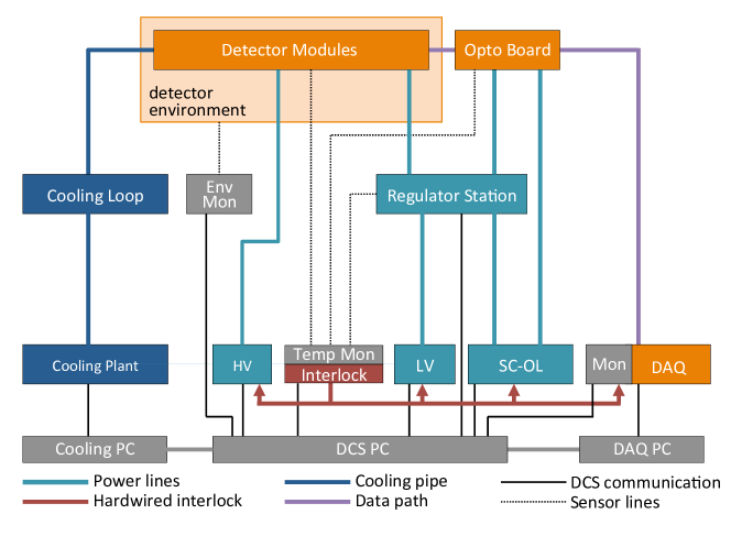
6.2.1 The DCS and interlock systems
The DCS has three main functions: to control the detector, the opto-board and the power supply operation; to monitor all operational and environmental aspects of the detector system; and to provide inputs to the power supply and interlock systems as needed for detector and operational security. Most parts of the DCS are provided by dedicated PCs located in the counting room, about from the ID. The regulator station at the PP2 panel and selected monitoring units are installed inside the detector cavern.
The main component of the IBL DCS software is a Finite State Machine (FSM) that is fully integrated into the DCS of the Pixel detector and ATLAS. The tree structure of the ATLAS FSM nodes reflects the structure of the detector. Commands are sent from the top node to its children, then the status information is sent back to the top node and informs the operator about the success of a command. As all modules of a half-stave are read out through a single opto-board, the half-stave is the key element of the IBL FSM. Because of the service modularity, four FE-I4B chips with their two (planar) or four (3D) sensors are the smallest units that can be separately steered by the DCS.
The interlock system is an independent hardware implementation complementary to the DCS. The core component of the interlock system is a flash FPGA with an internal Electrically Erasable Programmable Read-Only Memory (EEPROM) . This avoids the need of a program loading at power-on. A negative logic is implemented, which means that a missing cable or lost power causes an interlock automatically. Power supply and environmental (temperature and humidity) data are fed to the DCS, and the temperature data are independently fed to the interlock system. Additional information from the laser protection system, the cooling system, the LHC or other external systems is included into the interlock matrix. As this system is completely hardware based, maximum safety is provided.
6.2.2 The IBL power supplies
The detector modules and the opto-boards require dedicated powering, well adapted to the corresponding electrical loads. Common to all components is the use of floating power supplies with variable output voltages. The power supplies are controlled and monitored by the DCS, but essential security data such as over-current or high-temperature alerts are also transferred to the interlock system.
To deplete the sensors an HV power supply is required. While the planar sensors will require up to after irradiation, the 3D sensors can be operated with significantly lower voltages of a few hundred volts.
The FE-I4B chips are powered by the LV power supplies. Because of the large currents in the FE-I4B chip, the voltage drops on the services are non-negligible. The FE-I4B chips themselves require a nominal input voltage of , however the LV supply is able to deliver up to . Since the FE-I4B chips would be destroyed by voltages of greater than , a voltage regulator close to the detector is installed to protect the chips against transients. The output voltage of each regulator can be remotely programmed to deliver precise voltages to the FE-I4B chips, via a Controller Area Network (CAN) bus in 100 steps between to . The maximum deliverable current per channel is approximately and each channel is protected against sense line interruption compatible with the maximum voltage drop allowed in the system. The IBL regulator station is based on the design used in the other layers of the Pixel detector [4].
The Supply and Control of the Opto Link (SC-OL) is used to power the opto-boards and requires three different low voltages. For the main supply voltage, V, the SC-OL provides a maximum voltage of at a maximum current of . As the chips on the opto-board must also be protected, V is routed through the regulator station in the same way as the LV. The second supply voltage, V, biases the receiver PiN diodes. The supply voltage of up to provides a normal operation voltage of V of 5-10 V. The third supply voltage, V, with a maximum of , controls the current in the Vertical-Cavity Surface Emitting Lasers (VCSEL). Additionally, a reset signal is provided, which can be sent to the opto-board in case the decoder is stuck.
6.2.3 Temperature and humidity monitoring
The environmental monitoring is handled independently of the other monitoring tasks. Temperature sensors (NTCs) are installed in many different locations to protect detector components that might be damaged by overheating. Each Type 1 power bundle, serving a half-stave, includes fourteen or fifteen lines sending seven DCS signals to both the DCS monitoring units and the interlock system. Since the FE-I4B chips and silicon sensors can be permanently damaged by the overheating of detector modules, each sensor is also equipped with an NTC. A comparator sets a logical signal in case of overheating. In the same way, the opto-boards and the regulator station are equipped with NTCs. NTCs are also mounted on the cooling pipe and near the cable board. Finally, either a humidity sensor mounted on the cable board, or an NTC mounted on the cable bundle, is read out.
Several voltage and current diagnostic measurements as well as temperature sensors (diodes) are also built into the FE-I4B chips. An on-chip Analogue to Digital Converter (ADC) associated to an 8-to-1 analog Multiplexer (MUX) can be used to select and read out the temperature, power supply voltages, voltage references, detector leakage current, and other DCS analog voltages. On demand in calibration mode, this information can be sent to the DCS or through the standard data path. This monitoring strategy is not fully implemented for the IBL but remains a promising approach for future DCS developments, to reduce the material inside the detector volume.
6.3 Data Acquisition System (DAQ)
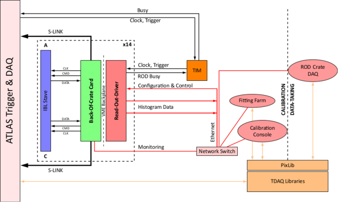
The IBL read-out system [15], shown in Figure 50, is based on the Pixel detector read-out [4]. Each IBL half-stave is connected via the opto-board [46] and a fibre bundle to the off-detector electronics boards: the Back-Of-Crate card (BOC) [12, 13] and the Read-Out-Driver (ROD) [11].
6.3.1 Optical link
The opto-board, shown in Figure 51, is connected to the counting room via approximately of optical fibre. On the BOC card clock and data signals are encoded into one Bi-Phase-Mark (BPM) signal, running at , which is sent to the opto-board via a single optical link serving as TTC link. At the same time, the detector modules generate data streams at using 8b/10b encoding. The data are then sent by the opto-board via one optical link per FE-I4B chip to the BOC card.
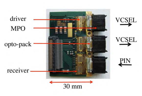
The opto-board handles data in both directions and provides eight receiver and 16 transmitter channels. Hence, each opto-board serves a half-stave (six planar modules and four 3D modules). Each opto-board therefore contains one PiN diode array and two VCSEL arrays, with each array containing 12 channels but only the inner 8 channels are used. The PiN diode array is paired to two 4-channel Digital Optical Receiver Integrated Circuits (DORIC). The PIN diode converts an optical signal into an electrical signal that the DORIC decodes the into clock and data signals. Both signals are then transferred in LVDS format to the module. Two 4-channel VCSEL Driver Chips (VDC), driving one VCSEL array with tunable current levels, are used to route the signals via the VCSELs to the BOC card. While the DORIC is a self-adjusting chip, the VDC requires an externally tunable voltage to steer the drive current and hence the optical output power of the VCSEL. The IBL uses 28 opto-boards and two additional boards are used for a Diamond Beam Monitor (DBM) [47].
6.3.2 Off-detector read-out electronics (ROD/BOC)
A ROD/BOC card pair is shown in Figure 52. As shown in Figure 50, data communication between the detector and the ROD/BOC cards is bi-directional: one control and two parallel data processing paths link the ROD/BOC pair to an IBL half-stave.
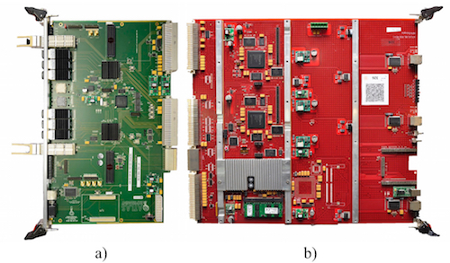
The ROD controls the detector operation for both the calibration and data-taking modes. All of the front-end commands, including the trigger and clock signals, are generated in the ROD using a Virtex-5 FPGA with an embedded PowerPC (PPC) processor. The trigger and clock signals are distributed to the ROD by the Trigger Timing Control (TTC) link from the TTC Interface Module (TIM). The ROD control signals are transmitted to the detector via the BOC. An FPGA running a MicroBlaze processor on each of the ROD and BOC cards handles the Ethernet connection between them. The BOC card is interfaced to the detector and to the ATLAS read-out system: the detector interface uses commercial SNAP12 optical transmitters and receivers343434The SNAP12 Multi-Source Agreement (May 2002) outlines specifications for the mechanical, electrical and optical interfaces of 12-channel pluggable parallel optical transmitter and receiver modules.; the read-out interface is via S-LINK connections353535 S-LINK, for simple link interface, is a high-performance data acquisition standard developed at CERN..
Each data processing path handles 16 FE-I4B chips and contains two FPGAs363636Unless otherwise specified, all FPGAs are from the XiLinx Spartan-6 family.: one on the BOC card, responsible for synchronising, decoding and processing the signal coming from the FE-I4B, and one on the ROD, which builds event fragments and packages them for transmission to the ATLAS read-out via QSFP transceivers373737The Quad Small Form-factor Pluggable (QSFP) is a hot-pluggable transceiver allowing data rates of 4x10 Gbit/s. on the BOC card. The FPGA on the ROD card is also responsible for generating the histograms used to calibrate the detector. These histograms are transmitted using the Ethernet protocol to a fitting farm that uses commercial PC processors. The boot and reset of the ROD is controlled by the Program Reset Manager (PRM) FPGA, directly mounted on the ROD.
A total of 15 ROD/BOC card pairs, 14 for the IBL staves and one for the DBM, are installed in a VME crate together with the TIM module which distributes the LHC clock and the ATLAS trigger signals. The loading of the ROD firmware and software as well as the transmission of control signals and data between the ROD and BOC is performed via the VME back plane; contrary to the Pixel detector read-out, the configuration of the cards and the transmission of calibration data are performed via Ethernet. As noted above, the fitting of calibration histograms is performed using a farm of PCs instead of the on-ROD Digital Signal Processors (DSPs) used for the Pixel detector read-out. This solution provides the scalability that is required to deal with the higher bandwidth of Run 2.
The IBL read-out hardware and system architecture is being implemented in stages to read the other Pixel detector layers because of the higher allowed bandwidth. The readout of the Pixel B-Layer is equipped with twice the number of optical links, and the upgrade of Pixel Layer 1 was made at the end of Run 1.
7 Interfaces and integration
The insertion of the IBL pixel layer was made possible by the reduction of the ATLAS beam-pipe diameter [6]. The inner radius was reduced from to , allowing sufficient radial space for the IBL and its mechanical support structure. The new beryllium beam pipe is described in Section 7.1, and the support structure is described in Section 7.2. Prior to insertion in the ATLAS experiment, the full IBL as well as its services were assembled around the beam pipe on the surface (Section 7.3) and electrically tested (Section 7.4) at room temperature. Once installed in the ATLAS cavern, electrical and environmental connections were made. In particular, the 2-phase CO2 cooling system as well as its connection to the IBL package and its subsequent performance is described in Sections 7.5 and 7.6.
7.1 The beryllium beam pipe
The new beam pipe was designed and fabricated with a length of , including the flanges (which were unchanged). The beryllium section is long with a nominal wall thickness of . It is installed symmetrically with respect to the interaction point. At each end of the beam pipe, split aluminium flanges of are welded, compatible with an insertion inside the IBL Inner Positioning Tube (IPT). The inner surface of the beam pipe is treated with a Non-Evaporable Getter (NEG) thin film coating to optimise the vacuum quality. The NEG coating is activated by heaters that are wrapped along the beam-pipe length for the bake-out. A bake-out is made each time the ultra-high vacuum is established. The heater temperature is monitored and controlled by thermo-couples installed along the beam pipe. To reduce possible damage to the IBL layer, the infra-red emissivity of the beam pipe is reduced by a surface layer of aluminium.
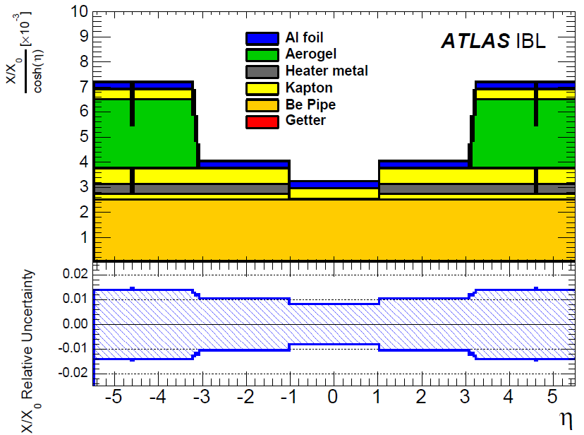
The composition and radiation length of the new beam pipe were both carefully validated. The thickness of the beryllium pipe was measured with a precision of for eight positions along each section of the pipe, and the average thickness was measured to be . The other components of the beam pipe (Kapton®, heater metal, aerogel, aluminium foil) were individually measured by 109Cd () X-ray absorption and their nominal composition and thickness were confirmed to within a few percent precision. The total uncertainty of the radiation length considers not only the material composition, but also fabrication details such as wrinkles of the Al foil.
As a result, the total thickness of the beam pipe was calculated to be at the centre of the beam pipe and up to at from the centre, as shown in Figure 53. The main reduction of material thickness was the removal of the aerogel insulating layer over a length of at the centre of the beam pipe.
As a cross-check, the fabricated beam pipe was scanned using X-rays at z positions of , , and along the beam pipe. The scanning equipment, shown in Figure 54, was mounted on a multi-purpose container (MPC; see Section 7.3) supporting the beam pipe.
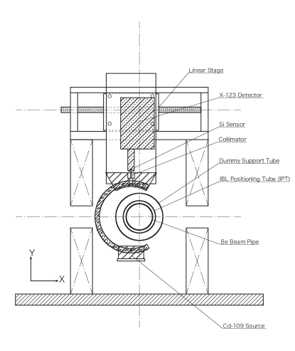
The X-ray assembly included a fully-depleted Si-PIN X-ray counter (Amptek X-123383838Amptek X-123 Si-Pin X-ray counter, see www.amptek.com) and a vertically collimated 109Cd source. The source and detector could slide together horizontally, maintaining a constant X-ray flux. The relative X-ray absorption at z = is shown in Figure 55 as a function of the horizontal position.
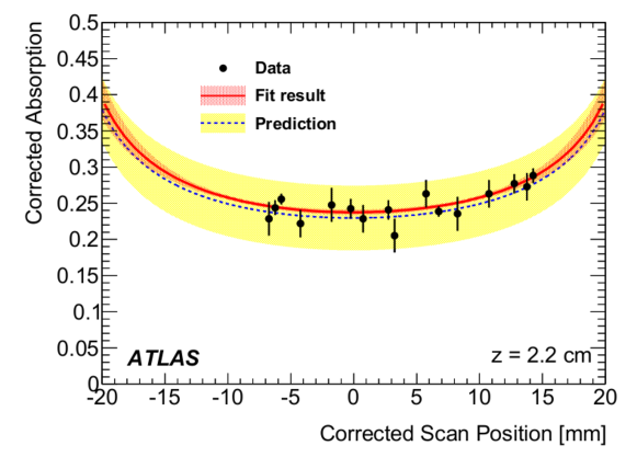
An X-ray absorption model, parameterising the absorption coefficient of the layers and the absolute X-ray flux, is in good agreement with the data. Similar validation results were obtained for z = and z = .
7.2 The inner mechanical structure of IBL and its external envelope
As shown in Figures 2 and 3, the IBL volume for the stave and services is delimited by the Inner Support Tube (IST), which is fixed on the Pixel structure, and by the IPT, which is a precision mechanical support to hold the staves and the services. A schematic and photograph of the IPT are shown in Figure 56.

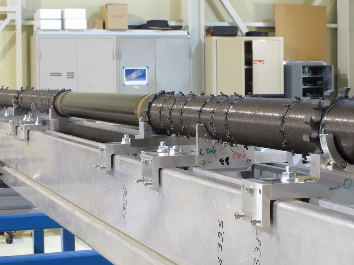
The IST is a long tube with an inner diameter of and wall thickness, containing the full IBL package and the central portion of the beam pipe. It is secured to each end of the Pixel detector frame in the PP0 area and to the pixel cruciforms in the PP1 region, located at respectively and from the interaction point along the beam axis. Given the clearance of only with respect to the Pixel B-Layer, the IST is designed to have a minimal deflection during its lifetime. It was therefore manufactured using very high modulus carbon fibre (K13), coupled with cyanate ester resin (RS3). The carbon-fibre material consists of seven -thick plies oriented in different directions to minimise the tube deflection. The thermo-mechanical behaviour of the complete package was precisely predicted by finite element analyses and validated with experimental data.
The IPT is a precision assembly of carbon fibre tubes and rings (Figure 56(a)) that aligns the 14 staves with high precision. The five carbon-fibre segments use the same carbon fibre material as the IST, but the central segment uses five plies to minimise the material budget; the resulting thickness is . In addition, to ensure electrical insulation with respect to the stave module HV, this central segment is co-cured with a -thick polyimide film. The service rings, each with 14 radial grooves for the stave services, are precisely positioned every along the IPT. A small extra length, estimated to be , compensates for the service cable contraction and extension during temperature excursions.
A key feature of the IPT design is the ability to perform a fast insertion or extraction of the IBL and of the beam pipe independently of the rest of the ATLAS ID. The IPT is locked in z with respect to the Pixel structure at a distance of from the interaction point on the C-side, and is positioned radially within the limited clearance to the IST, which is fixed to the Pixel frame. The beam pipe is positioned in z with respect to the LArg Cryostat at PP1, from the interaction point. It is positioned radially within the limited clearance to the IPT and the Liquid Argon cryostat at PP1.
Two titanium terminals are positioned at the IPT extremities. Their function is to provide shielding from electromagnetic interference, strain relief for the cooling fittings, space for cable bundle integration and mechanical stability during installation. The gluing of components on the IPT was performed using epoxy glue (Hysol 9394393939Hysol® is a trademark of Henkel Corporation, see www.henkel.com.) that can cure at room temperature and has a maximum service temperature of . This guarantees the integrity of all the parts, even during the beam-pipe bake-out when the maximum temperature is expected to reach at the contact points with the beam-pipe rings.
Two units were manufactured for each of the IST and the IPT and were surveyed in a metrology laboratory to check for geometrical defects and qualification. The best assemblies with respect to geometrical specifications were used for the IBL integration.
7.3 Surface integration and installation
The elements to be integrated can be grouped in three independent sets: the IPT with the support rings, the staves with their cooling pipes and the services.
The Multi-Purpose Container (MPC), the mechanical support for the IBL integration, was designed to allow secure and precise stave integration, and to transfer the IBL package to the experimental cavern. Initially, the beryllium part of the beam pipe was inserted inside the IPT. A precision tool was then used to transfer the staves from their holding jigs to the IPT, preserving the tight clearances with respect to the surrounding structures. After each stave was connected to the cooling extension (Section 7.6), it was fixed to the integration tool of the MPC (Figure 57). Using adjustable screws on the stave integration arm, and IPT rotations referenced with precision pins, each stave could be installed and transferred from the handling frame to the support ring of the IPT with a precision of over the length.
Once the 14 staves were loaded, a central ring consisting of seven parts was installed and clipped to the central stave support feet, providing an additional stiffening. However, because of stringent construction and thermal fixation constraints, it did not eliminate all possible detector degrees of freedom. It radially stiffens the 14 staves at the centre, while leaving free movement in the azimuthal direction and along the beam axis. Operationally, this resulted in an R- distortion of the staves at the level of a few / (Section 8.2).
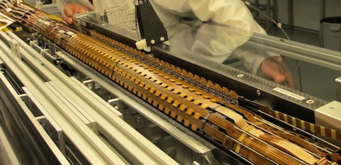
The services that connect the staves to each ID end, from the interaction point, were installed after the integration of each stave. The service installation consists of eight intermediate flex circuits linking Type 1 cables to the stave flex in the PP0 region (Section 6.1). The Type 1 cables service the HV and LV power, the read-out and the DCS signals and are laced in a single bundle that splits just before exiting the IBL volume into separate data and power bundles. After the installation of each stave and their services, electrical qualification tests were performed, before proceeding to the next row. All the staves were successfully integrated without rework or re-installation.
The next operation consisted of inserting soft sealing rings at the two extremities from the interaction region to guarantee a proper environment for the IBL. The IBL is flushed with dry nitrogen gas at a flow rate of up to . This ensures a dew point below that of the minimal foreseen coolant temperature of , keeping the detector dry under all operating conditions. The sealing ring core is moulded as a ring from polyurethane, with holes for electrical and cooling services. During cavern commissioning, the full dry nitrogen circuit, including sealing rings, was leak checked. At the nominal running parameters ( at at maximal overpressure), the measured outlet flow was , equivalent to a nitrogen circuit tightness of better than .
Once the integration was completed, the services (including an additional length of for the power bundle and for the data bundle) were packed to ensure the IBL envelope for installation in the ATLAS cavern. In particular, the Type 1 bundles from PP1 to PP2 were wrapped by a spiral wrapping tool around the beam pipe (Figure 58) until the IBL package was inserted inside the IST.
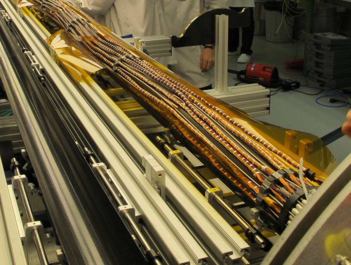
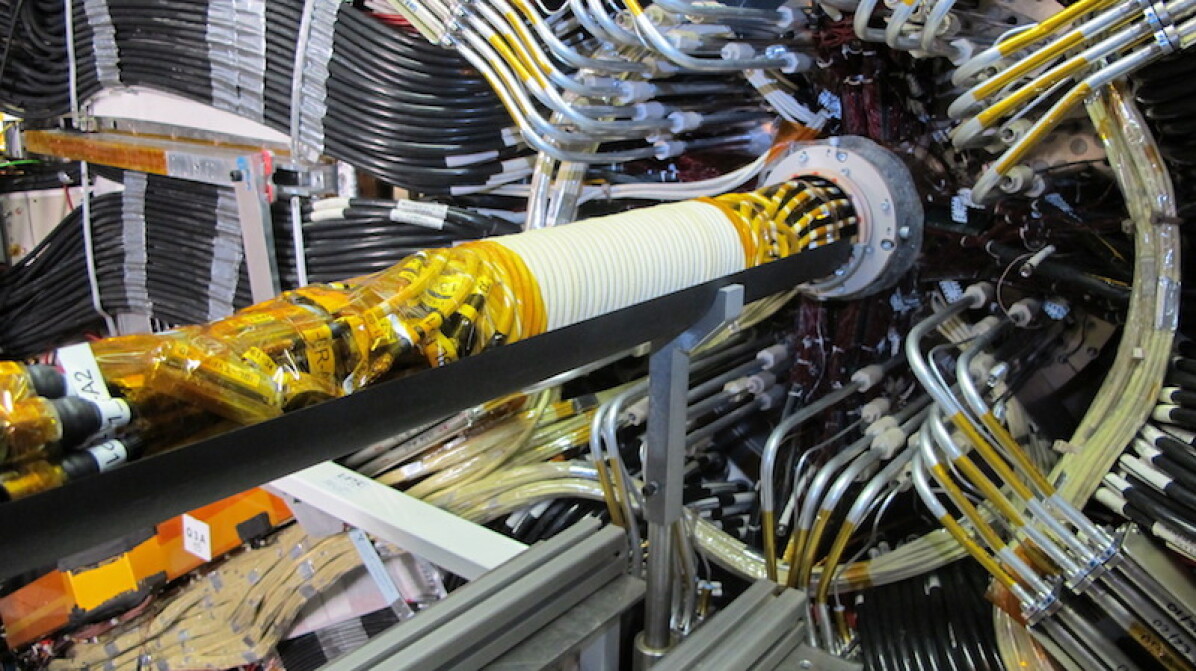
7.4 Electrical tests after stave integration.
The purpose of the stave electrical test after integration of the staves onto the IPT, cabling of the Type 1 cables and insertion inside the IST, was to verify the electrical and functional integrity of the stave components and to test the service chain. The stave test included threshold scans with and without sensor bias, a validation of the time-over-threshold (ToT) setting, and an I-V scan. The tests were directly compared to results obtained during the stave QA. A sample of these comparisons is shown in Figures 59, 60 and 61. Noise and threshold values are larger than in the stave QA because the detector was not cooled during the stave loading. This is especially true for 3D modules, which are more sensitive to temperature. With that caveat, no performance degradation was measured.
The tests also revealed several hardware problems (e.g. broken or shorted lines in the Type 1 cable or in the intermediate flex) that were repaired. The tests were repeated after sealing the IBL volume with two soft polyurethane disks, to check the correct functionality of all modules before wrapping the services and lowering the detector in the cavern of the ATLAS experiment. No changes with respect to previous tests were measured.

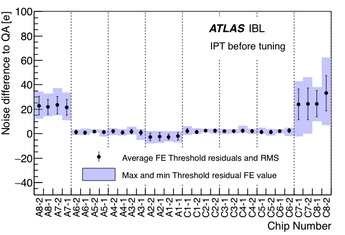
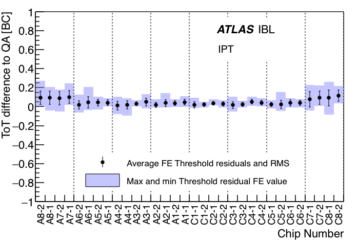
In parallel to the stave integration and test, a system test was prepared using two prototype IBL staves and either production or pre-production detector services, the full power and DCS chain, but mono-phase cooling. The measured noise, threshold and ToT performance were in excellent agreement with the QA. Scans were made using 241Am and 90Sr sources, as well as cosmic rays, with satisfactory results. The system test also confirmed the functionality of the interlock system. The system test setup continues to be used as a test-bench for operational maintenance and upgrades.
7.5 CO2 cooling system
The cooling of the IBL detector is based on CO2, which is circulated in a closed system through the detector with an overflow where part of the liquid is evaporated (approximately at ) [44]. The two-phase liquid-vapour mixture is returned to the cooling plant, which is located in the USA15 service cavern and easily accessible. The cooling plant condenses the returning two-phase CO2 using a commercial chiller. The liquid CO2 is pumped back to the manifold system near the IBL detector via a concentric transfer line that bridges the distance between the cooling plant in USA15 and the manifold in the UX15 service cavern. Figure 62 shows a simplified schematic of the IBL cooling system with the main components of the cooling system highlighted.
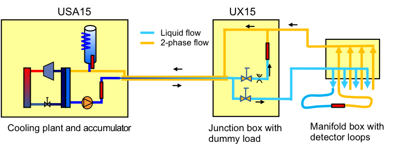
7.5.1 Cooling system operation
The CO2 arriving in the detector is a saturated liquid, which means that it evaporates directly when heat is applied. The temperature of the arriving saturated liquid is a function of the pressure, which is controlled by the cooling plant in USA-15. Changing the temperature of the two-phase mixture in the accumulator will change the pressure in the system and allows operation with an evaporation temperature between (used for commissioning) and .
The pressure can also be increased to fully liquify the system. This is used at start-up to prevent thermal shocks. The cool-down temperature ramp is controllable and can be set to per minute, or to a lower rate. The preferred inlet condition of the cooling is that the liquid is saturated in the IBL stave region, so that heat needs to be applied to the cold liquid. This heat is taken out of the returning two-phase mixture by a constant thermal contact of the liquid inlet and the two-phase return. The inlet and outlet fluids circulate in concentric tubes (the inlet liquid in a inner diameter tube, and the outlet fluid circulating in a outer diameter tube). The actual system allows having the same temperature at the detector and at the two-phase temperature controlled by the accumulator. The higher pressure on the inlet keeps the CO2 liquified at the inlet to the cooling tubes. It starts boiling in the cooling tubes of the IBL staves once powered. This liquid temperature condition works over a large range of operational temperatures and makes the control of the system, without active elements inside the ATLAS detector, very reliable in a hard-to-access region. The first tests allowed the system to reach stable temperatures for various heat loads and was tested up to a thermal load of and down to (Figure 63).
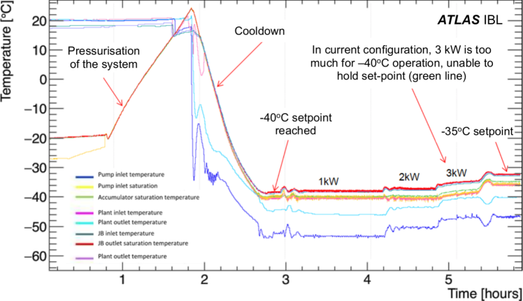
7.5.2 Redundant system
Once irradiated, the IBL must remain cold at all times to limit the radiation damage in the silicon sensors. To guarantee a fail-safe solution for the CO2 cooling a redundant system has been developed. There are two identical plants where one serves as a full back-up of the running plant. Each plant has its own control and sensor system with a dedicated Programmable Logic Controller (PLC) and power source. The transfer lines and the accumulator are shared with respect to the CO2 volume. A plant can be disconnected from the main system for interventions. Both chillers are cooled by water provided from the central ATLAS water system. An integrated air cooling condenser is present in each chiller unit to back-up the single source water cooling. During operation, one system can remain on standby for a fast switch-over in case of a system failure. In addition, for greater safety, the two plants can operate in parallel increasing the cooling capacity, but this operational mode is mainly foreseen for the beam-pipe bake-out.
7.5.3 Detector distribution
A homogeneous CO2 flow distribution to the 14 IBL staves is achieved by 11 m long lines and inner diameter capillaries (Figure 64). These capillaries are routed inside the return tubes of the IBL to be shielded from ambient heating. The manifolds are located in the muon detector area. The total tube length from manifold through the IBL and back to the return manifold is approximately ( concentric tubing, connection tube and stave tube). The inlet tubes, the boiling channels and outlet tubes have nominal inner diameters of , and respectively. The innovative vacuum isolated flexible lines were used for the fluid transfer on long distances [44]. The concentric return tubes in the flexible transfer line have a diameter of . The concentric line is outside of the ID volume and is insulated by multilayer insulation inside a diameter vacuum metallic tube. This triple concentric assembly is flexible and is routed similarly to the electrical cabling, through the ID end plate region towards the manifold. The flex lines inside the ATLAS ID end plate up to the splitter box are shown on Figure 64(b).

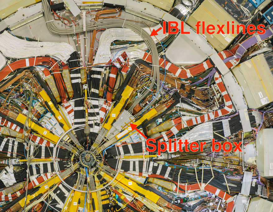
7.5.4 Commissioning
The commissioning of the system started in January 2014 with local circulation of CO2 using the plant internal dummy load. Near the manifold the so-called junction box is present (Figure 64) where the flow can be by-passed through a dummy load. The system commissioning was made using this dummy load with a restriction valve having a similar flow resistance to that of the detector loops. One of the main challenges for the IBL cooling was related to the colder temperatures compared to previous cooling systems. The requirement of cooling to brings the margin close to the CO2 freezing point () and hence a very stable primary cooling was needed. In the early phase the system was tuned such that under extreme conditions it remained within safe operational boundaries. The measured heat load was approximately at and at . The IBL detector was also successfully tested during the commissioning at various temperatures with the nominal power load expected during operation. The boiling onset inside the IBL cooling loops sometimes had problems to be correctly initiated. In this case, super-heated liquid, that is warmer than the boiling temperature and has a worse heat transfer than the desired two-phase flow, could be present in the detector. As a result, the temperatures of the first modules of a stave were sometimes a few degrees higher. To mitigate this problem, flow restrictions were applied in the inlet manifold to reduce the flow and to keep the inlet pressure high [44].
7.6 On-detector cooling branch and interfaces
The on-detector cooling branches consist of a length straight section of titanium pipe with two brazed junctions at each side of the stave and a dis-mountable fitting at each end (Figure 65). As for the rest of the IBL services, the detector side of the fitting must respect the insertion envelope. The branch is connected on each side to a short 90 ∘-bend section of Ti pipe, which is brazed to an electrical break and to a stainless steel pipe at the other end. The stainless steel pipes are then routed on a path specific to each stave to a splitter box where the transition is made to flexible vacuum transfer lines of length connected to a manifold box further out from the ID.
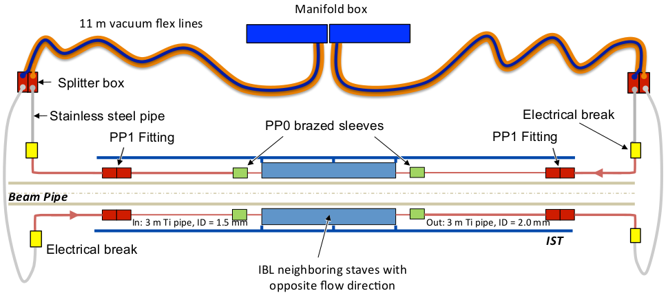
7.6.1 Fittings outside the IBL volume
Because of space constraints for the insertion of the IBL inside the IST, the electrical and cooling service envelope is restricted to a maximum external radial space of . An industrial fitting of such a small size compatible with the pressure, the radiation hardness, and the reliability requirements of the IBL does not exist; therefore a custom fitting was developed.
The use of the CO2 evaporative system (Section 7.5) together with titanium as a selected material for both the tube and the fitting required a special engineering and design development to maximise the reliability. The extreme radiation environment excludes the use of organic joints, leading to a metal-to-metal contact solution. The requirement led to the selection of a hard titanium alloy (TA6V, or grade 5) to guarantee the sealing. The tightness is ensured by a cone-sphere junction, with strict requirements on the surface quality.
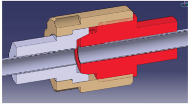
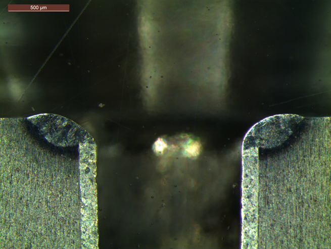
Prototype fittings were assessed with several batches of 10 fittings machined in-house and tested to qualify the final design. The final production batches were manufactured in industry and qualified in-house on a large number of test samples. The fitting is connected to the thin titanium pipe ( wall thickness) by electron beam welding at the front face (Figure 66). This welding requires high quality vacuum and was performed in industry. The method imposes strict requirements on the reliability of the fitting which can not be repaired. A large-scale qualification and validation campaign was carried out, with 100 fittings leak tested, some of them mated and de-mated tens of times. An industrial qualification procedure was applied to fulfil the standard requirements with large statistics pressure cycling. A set of ten fittings, electron-beam welded to short-pipe sections and connected in series, was tightened by the collaboration and sent to a certified ISO qualification lab to perform the pressure cycling (one million water cycles with to at ). The entire set successfully passed the leak tests. The minimal torque required for reliable tightening was determined during the qualification campaign. A torque was sufficient to guarantee the success of tests like fast temperature cycling or thermal shocks using a CO2 blow-off system. A small subset of fittings was tested at higher torque up to without visible damage. The final torque used for installation in the cavern was for which all the 28 IBL connections passed the pressure tests at .
The pre-series consisted of producing approximately 100 samples for qualification. The 28 fittings selected for installation were visually inspected for scratches and dust, and individually leak-tested.
7.6.2 The cooling line electrical break
The grounding and shielding scheme of the IBL requires using electrical breaks on the cooling pipes at the PP1 area (Figure 67) and in the ID end-flange region. Because of space constraints the closest possible location was just after the 90 ∘-bend of the radial section of the pipe. The mechanical stress in this section is significant; a relatively large diameter () ceramic electrical break was chosen for robustness. At this location it is also necessary to make the transition from titanium pipes, which are difficult to bend, to stainless steel pipes, which are easily routed. After testing several options for the titanium to stainless steel transition the most reliable solution found was to braze in the same processing step a stainless steel sleeve on the external side of the ceramic of the electrical break (the detector side of the ceramic being brazed in a titanium sleeve). Due to the mismatch of the thermal expansion coefficient between the ceramic and the stainless steel material the brazing is a delicate process. A full qualification in collaboration with industry was performed to design and produce a reliable junction. The qualification process was the same as for the fitting and a number of destructive tests were made to evaluate the mechanical robustness and the capillary penetration of the brazing material. All the tests were passed successfully and the tensile tests at the electrical break junction revealed that the pipe was weaker and that the junction withstands at least internal pressure (limited by the test setup). In addition, a few electrical break samples were irradiated to with a electron beam, corresponding to the expected maximum end-of-life IBL ionising dose, and found to be leak-tight.
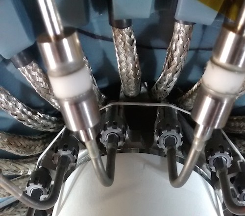
7.6.3 The brazing junction of the stave inside the detector volume
At PP0, the cooling junction connects the staves to the cooling extension running from to (PP1 region) from the interaction point. This junction was designed such that the stave production could be made with long objects, easing the module loading task, the testing tool, the handling and the shipment. Due to the limited space around the beam pipe in the PP0 region, and the high level of reliability required inside the detector volume, the use of fittings was not possible.
One major impact of this design choice was to develop a thin wall
()
titanium pipe joining technique between the extension and the stave pipe which could be easily connected after module loading and before integration of the staves around the IPT. When such an operation is performed after the module loading, the requirements are not only based on the quality of the welded junction but also the risk of damage to electrical or mechanical components (that should be negligible). Therefore techniques that require excessive heat spread, such as oven brazing, or high and fast current spikes such as orbital welding, were prohibited.
With such a thin wall thickness, titanium
is not an easy material to weld or braze. Since it is highly sensitive to oxygen, welding or brazing requires an inert environment, e.g. argon, or vacuum. Induction welding was the only technique (Figure 68) found that uses local heating, does not involve current spikes on mechanical structures, and has a reasonably sized tool that does not risk damage to the front-end electronics.
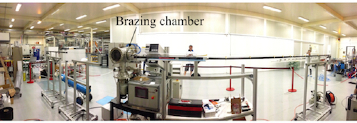
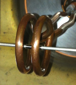
The brazing compound or filler used was Palcusil-5 (Ag , Cu , Pb ). The brazing process was performed at to in vacuum ( ) for several seconds, with a well defined ramp-up (Figure 69). Prior to the chamber and the pipe vacuum pumping, argon is flushed to minimise the presence of oxygen around the brazing point.
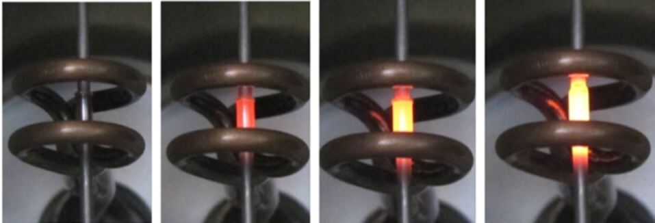
Qualification tests were performed to fine-tune the parameters and to check the quality and reliability of the braze. All test samples underwent visual inspection, leak tests, thermal shocks, metallographic inspection, tensile tests and thermal cycling. The 14 IBL staves were successfully brazed on both sides and no damage was detected on any of the modules loaded on staves. The most delicate part of the process was to design and manufacture the feedthrough and sealing parts on the vacuum brazing chamber, given such thin pipes and the high level of vacuum required to complete the junction.
8 Final remarks and conclusion
The construction of the IBL detector started in mid-2012 and the completed detector was installed in May 2014. Because of the demanding detector constraints, and the hostile radiation and operational environment, R&D programs relevant to the IBL started in 2008. IBL commissioning in the ATLAS cavern started in June 2014 and the IBL was fully commissioned from November 2014.
8.1 The IBL challenges
Key challenges of the IBL project included:
-
-
The R&D, industrialisation and integration of two sensor technologies (planar and 3D) on one single-stave layout, capable of surviving integrated radiation doses of up to , and with inactive edges of order . The successful development of planar sensors with small inactive edges capable of reliable and efficient operation at full depletion after large radiation doses was an essential requirement for IBL operation. The new 3D sensor technology is being used for the first time in a tracking detector. The radiation tolerance of 3D sensors has been demonstrated, and their reliable and efficient operation in the IBL is a major milestone because of their reduced operating voltage (and power consumption) after high radiation doses;
-
-
The bump-bonding of thinned FE-I4B chips to the planar and 3D sensors. This requirement was met by gluing a sapphire glass substrate to the FE-I4B wafer for all the processing steps and later detaching it using a laser de-bonding technique after the bump-bonding and before further module assembly;
-
-
The development of the FE-I4B front-end read-out chip, the largest front-end design in radiation hard CMOS technology for a tracker in particle physics. Its large area maximises the active area and reduces the bump-bonding cost;
-
-
The global IBL envelope of less than between the Pixel detector and the beam pipe was a challenge for integration, installation and the beam-pipe bake-out. As a result, innovative and custom-made mechanical supports, services and fittings were developed.
-
-
The aggressive design minimisation of the stave material budget, and the space constraint above, required that the service bus was tightly integrated with the stave (with implications for thermal expansion mismatches that are noted below). An on-stave flex having two aluminium layers for power and four copper layers for service lines was developed;
-
-
The development of Type 1 electrical services for the power distribution, and long () data transmission wires, because of the tight space requirements and the hostile radiation environment. The high-density pin connectors were designed and fabricated specifically to match the limited space for integration;
-
-
The optimisation of the thermo-mechanical interface between the module and the local stave support to guarantee the interface reliability and reproducibility, radiation hardness, and the replaceability of a module without damaging neighbouring modules, the stave itself or the service flex integrity;
-
-
The design, development and qualification of cooling pipe connections and electrical insulation for proper grounding and shielding;
-
-
The development of reliable CO2 cooling in the detector region while satisfying the space and thermal insulation requirements. This required the R&D, design and fabrication of flexible vacuum transfer lines; these could not be transferred to industry for logistic reasons and were produced in-house;
-
-
Extreme sealing and insulation capabilities, given the low dew-point temperature inside the detector volume, with CO2 cooling close to the CO2 freezing point ();
-
-
Installation of the cooling plant and the long vacuum transfer line () to the junction box and a dummy load installed close to the IBL and inside the Muon detector. Two cooling plants, each with a maximum load, are installed and independently controlled such that they can run either in complementary operational mode, one in standby while the other is operational, or in parallel which was mainly used during the bake-out of the beam pipe.
The successful development of both the planar sensor technology and the new 3D sensor technology, capable of reliable and efficient operation in the IBL after high radiation doses, is a major milestone in the demonstration of their suitability for tracking detectors at the HL-LHC. The lower operating voltage of 3D sensors after high radiation doses is a significant potential advantage for HL-LHC operation.
During the IBL production and integration, two major issues affected the schedule. The first issue concerned the bump-bonding yield for the initial production batches. An excess of merged and open bumps (Section 3.5) was identified to result from the solder flux used for bump bonding. The problem was resolved after a change of the tacking material and of the flip-chip machine. The second issue concerned wire-bond corrosion [42], which was identified on most staves mid-way during the production (Section 5.4). This resulted from a combination of extreme susceptibility to corrosion and accidental exposure to humidity during the temperature cycling tests after stave loading, and all but two staves could be fully repaired. Two options were considered to protect against potential future corrosion: the potting of the bond foot or the use of spray coating such as polyurethane, but neither were possible because of the schedule. It was decided to leave the IBL detector with unprotected wire bonds and to guarantee at all stages of the integration, installation and operation phases a safe humidity level.
8.2 IBL in ATLAS
The commissioning of the IBL as part of the ATLAS experiment closely followed the on-surface QA procedure. Initially, the integrity of the LV sense lines for each module group was ensured. The modules were then powered with their nominal supply voltage. At each step, voltage and current readings were compared to the measurements on-surface QA. After verification of the expected DCS measurements, configuration commands were sent to the FE-I4B chips to establish communication with the modules. These powering and configuration tests were followed by digital, analog, threshold and ToT scans, and finally re-tuning of the threshold and the ToT. The RCE read-out system was used for this initial commissioning in the cavern, to ensure a consistent comparison with the on-surface QA. The results confirmed 100% damage-free transportation and installation of the IBL before the sealing of the inner detector volume at the end of July 2014.
The commissioning of the ROD/BOC read-out system started in August 2014. Nine of the 14 IBL staves were integrated in the ATLAS experiment for the collection of cosmic ray data in October 2014. Subsequently, the new beryllium beam pipe was heated to to activate the NEG coating necessary to achieve the high vacuum levels required for LHC operation. The CO2 cooling system ensured the safety of the IBL during this bake-out. From November 2014, the IBL was fully integrated as part of the ATLAS experiment.
Details of the ATLAS commissioning, data taking and performance are beyond the scope of this paper [48]. However, four detector issues related to the design and construction of the IBL are briefly noted below. None have affected the quality of data from the IBL, nor the physics performance.
-
-
Since the wire bonds were not encapsulated, and the IBL operates in a 2 T magnetic field, current changes during the read-out may risk damage from bond oscillations [49]. To avoid oscillation frequencies a Fixed Frequency Trigger Veto was implemented at the DAQ level in the range 3 to 40 KHz;
-
-
As noted in Sections 5.4 and 8.1, wire bond corrosion was identified on most staves during mid-production, because of accidental exposure to humidity at low temperature during temperature cycling. Because of schedule considerations, it was decided to ensure that the staves remain at low humidity. The performance of the staves has not deteriorated following this precaution;
-
-
An increase in the current consumption of the FE-I4B chip at low total ionising dose was identified to result from N-MOS transistor leakage currents after the build-up of charge at the SiO2 interface in the 130 nm CMOS process [50]. The evolution of this current was evaluated at different temperatures and annealing procedures were introduced by operating the detector at temperatures around ;
-
-
Distortions resulted from the R- twisting of staves at the level of a few /, due to the mismatch of the thermal expansion coefficient between the stave and the stave flex, and the asymmetric attachment of the flex that was made necessary by mechanical constraints [51]. The impact of this is minimised by ensuring a temperature stability of less than and by the development of in-run alignment correction procedures.
8.3 Conclusion
The fabrication and integration of the ATLAS IBL detector is described in this paper. A fully working detector with only 0.09% of dead channels was successfully installed in ATLAS in May 2014 and fully commissioned as part of the ATLAS detector in November 2014. The addition of this innermost pixel layer, very close to the interaction point and with a smaller pixel size than other Pixel layers, provides additional redundancy and significantly improves the ATLAS tracking and vertexing performance.
Acknowledgements
We acknowledge the support of NSERC, NRC and CFI, Canada; CERN; MSMT CR, MPO CR and VSC CR, Czech Republic; IN2P3-CNRS, CEA-DSM/IRFU, France; BMBF, HGF, and MPG, Germany; INFN, Italy; MEXT and JSPS, Japan; NWO, Netherlands; RCN, Norway; MES of Russia and NRC KI, Russian Federation; ARRS and MIZŠ, Slovenia; MINECO, Spain; SRC and Wallenberg Foundation, Sweden; SERI, SNSF and Cantons of Bern and Geneva, Switzerland; MOST, Taiwan; STFC, United Kingdom; NSF MRI award PHY-1039175 and DOE, United States of America.
In addition, individual groups and members have received support from the FP7 Marie Curie Initial Training Network program and the Talent program (http://talent.web.cern.ch/TALENT/index.shtml) of the European Union.
A close collaboration with the silicon sensor suppliers, during the R&D and procurement phases, was essential to the success of the project and is gratefully acknowledged: CiS Forschungsinstitut fr Mikrosensorik und Photovoltaik GmbH, Erfurt, Germany; FBK Fondazione Bruno Kessler, Povo di Trento, Italy; CNM Centro Nacional de Microelectronica, Barcelona, Spain. The successful development of new techniques for the bump-bonding of thin wafers by Fraunhofer IZM, Berlin, Germany, was essential to the project and is gratefully acknowledged. The work of a dedicated task force to recommend a production and operation strategy for staves susceptible to wire bond corrosion is gratefully acknowledged. We thank the CERN DSF (Detector Silicon Facility) for their contribution to the rework of IBL staves affected by wire bond corrosion.
We acknowledge CERN and the ATLAS Collaboration, and in particular the ATLAS TC (Technical Coordination) and CERN EP-DT groups, for their support during the construction and integration of the ATLAS IBL detector. We further acknowledge the support staff from participating IBL institutes, who were essential to the success of the project.
References
- [1] ATLAS Collaboration “The ATLAS Experiment at the CERN Large Hadron Collider” In JINST 3, 2008, pp. S08003 DOI: 10.1088/1748-0221/3/08/S08003
- [2] Lyndon Evans and Philip Bryant “LHC Machine” In JINST 3, 2008, pp. S08001 DOI: 10.1088/1748-0221/3/08/S08001
- [3] ATLAS Collaboration “The ATLAS Inner Detector commissioning and calibration” In Eur. Phys. J. C70, 2010, pp. 787–821 DOI: 10.1140/epjc/s10052-010-1366-7
- [4] G. Aad “ATLAS pixel detector electronics and sensors” In JINST 3, 2008, pp. P07007 DOI: 10.1088/1748-0221/3/07/P07007
- [5] T. Heim “Status and performance of the ATLAS Pixel Detector after 3 years of operation” In Nucl. Instrum. Meth. A 765, 2014, pp. 227–231 DOI: http://dx.doi.org/10.1016/j.nima.2014.04.058
- [6] ATLAS Collaboration “ATLAS Insertable B-Layer Technical Design Report”, CERN-LHCC-2010-013, ATLAS-TDR-19, 2010
- [7] ATLAS Collaboration “Technical Design Report for the ATLAS Inner Tracker Strip Detector”, CERN-LHCC-2017-005, ATLAS-TDR-025, 2017
- [8] M. Barbero “Submission of the First Full Scale Prototype Chip for the Upgraded ATLAS Pixel Detector at LHC, FE-I4A” In Nucl. Instrum. Meth. A 650, 2011, pp. 111–114 DOI: http://dx.doi.org/10.1016/j.nima.2010.11.131
- [9] J. Albert “Prototype ATLAS IBL modules using the FE-I4A front-end readout chip” In JINST 7, 2012, pp. P11010 DOI: 10.1088/1748-0221/7/11/P11010
- [10] ATLAS Collaboration “Study of the material of the ATLAS inner detector for Run 2 of the LHC”, 2017 arXiv:1707.02826 [hep-ex]
- [11] A. Gabrielli “Firmware development and testing of the ATLAS Pixel Detector / IBL ROD card” In JINST 10.03, 2015, pp. C03037 DOI: 10.1088/1748-0221/10/03/C03037
- [12] M. Wensing “Firmware development and testing of the ATLAS IBL Back-Of-Crate card” In Proceedings, 3rd International Conference on Technology and Instrumentation in Particle Physics (TIPP 2014): Amsterdam, Netherlands, June 2-6, 2014 TIPP2014, 2014, pp. 216
- [13] M. Wensing “Testing and firmware development for the ATLAS IBL BOC prototype” In JINST 7, 2012, pp. C12027 DOI: 10.1088/1748-0221/7/12/C12027
- [14] S. Kersten “Detector Control System of the ATLAS Insertable B-Layer” In Proceedings 13th International Conference on Accelerator and Large Experimental Physics Control Systems, Grenoble, 2011
- [15] A. Polini “Design of the ATLAS IBL Readout System” In Phys. Procedia 37, 2012, pp. 1948–1955 DOI: 10.1016/j.phpro.2012.02.524
- [16] Karolos Potamianos “The upgraded Pixel detector and the commissioning of the Inner Detector tracking of the ATLAS experiment for Run-2 at the Large Hadron Collider” In Proceedings, 2015 European Physical Society Conference on High Energy Physics (EPS-HEP 2015): Vienna, Austria, July 22-29, 2015 EPS-HEP2015, 2015, pp. 261 arXiv:1608.07850 [physics.ins-det]
- [17] ATLAS Collaboration “A neural network clustering algorithm for the ATLAS silicon pixel detector” In JINST 9, 2014, pp. P09009 DOI: 10.1088/1748-0221/9/09/P09009
- [18] ATLAS Collaboration “The Optimization of ATLAS Track Reconstruction in Dense Environments”, ATL-PHYS-PUB-2015-006, 2015 URL: http://cds.cern.ch/record/2002609
- [19] M. Cacciari “The anti- jet clustering algorithm” In JHEP 04, 2008, pp. 063 DOI: 10.1088/1126-6708/2008/04/063
- [20] ATLAS Collaboration “Performance of b-jet identification in the ATLAS experiment” In JINST 11, 2016, pp. P04008 URL: http://stacks.iop.org/1748-0221/11/i=04/a=P04008
- [21] ATLAS Collaboration “Expected performance of the ATLAS -tagging algorithms in Run-2”, ATL-PHYS-PUB-2015-022, 2015 URL: http://cds.cern.ch/record/2037697
- [22] S. Parker, C. Kenney and J. Segal “3-D: A New architecture for solid state radiation detectors” In Nucl. Instrum. Meth. A 395, 1997, pp. 328 DOI: http://dx.doi.org/10.1016/S0168-9002(97)00694-3
- [23] T. Wittig “Slim Edge Studies, Design and Quality Control of Planar ATLAS IBL Pixel Sensors”, 2013 URL: http://dx.doi.org/10.17877/DE290R-5402
- [24] S. Altenheiner “Planar slim-edge pixel sensors for the ATLAS upgrade” In JINST 7, 2012, pp. C02051 URL: http://stacks.iop.org/1748-0221/7/i=02/a=C02051
- [25] C. Goessling “Evaluation of the breakdown behaviour of ATLAS silicon pixel sensors after partial guard-ring removal” In Nucl. Instrum. Meth. A 624, 2010, pp. 410–413 DOI: http://dx.doi.org/10.1016/j.nima.2010.06.004
- [26] G. Pellegrini “First double-sided 3-D detectors fabricated at CNM-IMB” In Nucl. Instrum. Meth. A 592, 2008, pp. 38 DOI: http://dx.doi.org/10.1016/j.nima.2008.03.119
- [27] A. Zoboli “Double-Sided, Double-Type-Column 3-D Detectors: Design, Fabrication, and Technology Evaluation” In IEEE Transactions on Nuclear Science 55.5, 2008, pp. 2775 DOI: 10.1109/TNS.2008.2002885
- [28] G. Giacomini “Development of Double-Sided Full-Passing-Column 3D Sensors at FBK” In IEEE Transactions on Nuclear Science 60.3, 2013, pp. 2357 DOI: 10.1109/TNS.2013.2262951
- [29] G. Pellegrini “3D double sided detector fabrication at IMB-CNM” In Nucl. Instrum. Meth. A 699, 2013, pp. 27 DOI: http://dx.doi.org/10.1016/j.nima.2012.05.087
- [30] M. Povoli et al. “Slim edges in double-sided silicon 3D detectors” In Proceedings, 13th International Workshop on Radiation imaging detectors (IWORID2011) 7, 2012, pp. C01015 DOI: 10.1088/1748-0221/7/01/C01015
- [31] Gerhard Lutz “Semiconductor Radiation Detectors: Device Physics” New York: Springer, 1999 URL: http://www-spires.fnal.gov/spires/find/books/www?cl=QC787.C6L88::1999
- [32] T. Hemperek “Digital Architecture of the New ATLAS Pixel chip” In IEEE NSSCR N13-179, 2009, pp. 791 DOI: 10.1109/NSSMIC.2009.5402304
- [33] V. Zivkovic “The FE-I4 pixel readout system-on-chip resubmission for the insertable B-Layer project” In JINST 7, 2012, pp. C02050 DOI: 10.1088/1748-0221/7/02/C02050
- [34] M. Backhaus “Characterization of the FE-I4B pixel readout chip production run for the ATLAS Insertable B-layer upgrade” In JINST 8, 2013, pp. C03013 DOI: 10.1088/1748-0221/8/03/C03013
- [35] M. Menouni “SEU tolerant memory design for the ATLAS pixel readout chip” In JINST 8, 2013, pp. C02026 URL: http://stacks.iop.org/1748-0221/8/i=02/a=C02026
- [36] M. Karagounis “An integrated Shunt-LDO regulator for serial powered systems” In Proceedings of ESSCIRC ’09, 2009, pp. 276–279 DOI: 10.1109/ESSCIRC.2009.5325974
- [37] L. Gonella “The Shunt-LDO regulator to power the upgraded ATLAS pixel detector” In JINST 7, 2012, pp. C01034 DOI: 10.1088/1748-0221/7/01/C01034
- [38] M. Backhaus “Development of a versatile and modular test system for ATLAS hybrid pixel detectors” In Nucl. Instrum. Meth. A 650, 2011, pp. 37 DOI: 10.1016/j.nima.2010.12.087
- [39] D.-L. Pohl “Overview of the ATLAS Insertable B-Layer (IBL) Project” In Proceedings of Science (RD13) 012, 2014 URL: https://pos.sissa.it/189/012/
- [40] J. Bilbao de Mendizabal et al. “Irradiation of an IBL stave in a 10 MeV beta beam”, 2013 URL: https://cds.cern.ch/record/1557832
- [41] ATLAS Collaboration “IBL Module Loading onto Stave and Quality Check”, 2015 URL: https://cds.cern.ch/record/2110639
- [42] ATLAS Collaboration “ATLAS Pixel IBL: Stave Quality Assurance”, 2014 URL: http://cds.cern.ch/record/1754509
- [43] T. Kohriki “First observation of thermal runaway in the radiation damaged silicon detector” In IEEE Transactions on Nuclear Science 43.3, 1996, pp. 1200 DOI: 10.1109/23.506663
- [44] B. Verlaat “The ATLAS IBL CO2 cooling system” In JINST 12.02, 2017, pp. C02064 DOI: 10.1088/1748-022/12/02/C02064
- [45] R. Bartoldus “A new ATLAS muon CSC readout system with system on chip technology on ATCA platform” In JINST 11.01, 2016, pp. C01059 DOI: 10.1088/1748-0221/11/01/C01059
- [46] K.. Gan “Design, production, and reliability of the new ATLAS pixel opto-boards” In JINST 10, 2015, pp. C02018 DOI: 10.1088/1748-022/10/02/C02018
- [47] M Červ “The ATLAS Diamond Beam Monitor” In JINST 9, 2014, pp. C02026 URL: http://stacks.iop.org/1748-0221/9/i=02/a=C02026
- [48] ATLAS Collaboration “ATLAS Pixel Performance (to be published)”, 2017
- [49] D. Alvarez Feito et al. “Studies of IBL wire bonds operation in a ATLAS-like magnetic field.”, 2015 URL: http://cds.cern.ch/record/2010249
- [50] ATLAS Collaboration “Radiation induced effects in the ATLAS Insertable B-Layer readout chip”, 2017 URL: https://cds.cern.ch/record/2291800
- [51] ATLAS Collaboration “Alignment of the ATLAS Inner Detector with the initial LHC data at = 13 TeV”, ATL-PHYS-PUB-2015-031, 2015 URL: http://cds.cern.ch/record/2038139