Linear-in-frequency optical conductivity in GdPtBi due to transitions near
the triple points
Abstract
The complex optical conductivity of the half-Heusler compound GdPtBi is measured in a frequency range from 20 to 22 000 cm-1 (2.5 meV – 2.73 eV) at temperatures down to 10 K in zero magnetic field. We find the real part of the conductivity, , to be almost perfectly linear in frequency over a broad range from 50 to 800 cm-1 ( 6 – 100 meV) for K. This linearity strongly suggests the presence of three-dimensional linear electronic bands with band crossings (nodes) near the chemical potential. Band-structure calculations show the presence of triple points, where one doubly degenerate and one nondegenerate band cross each other in close vicinity of the chemical potential. From a comparison of our data with the optical conductivity computed from the band structure, we conclude that the observed nearly linear originates as a cumulative effect from all the transitions near the triple points.
Heusler materials are currently well recognized for their wide range of spectacular electronic and magnetic properties Wollmann2017 . The high tunability of these compounds allows designing materials with properties on demand for future functioning applications Manna2018 ; Casper2012 . Recently, band inversion and topologically nontrivial electronic states have been intensively studied in (half-)Heusler compounds with strong spin-orbit coupling (SOC) Chadov2010 ; Lin2010 ; Xiao2010 ; Al-Sawai2010 ; Liu2011 ; Liu2016 ; Logan2016 ; Shekhar2016 .
Among other half-Heusler compounds with strong SOC, GdPtBi occupies a special place: the hallmarks of a Weyl-semimetal (WSM) state, such as negative magnetoresistance and the planar Hall effect, are vividly developed in this material and are assigned to manifestations of the chiral anomaly Hirschberger2016 ; Liang2018 ; Kumar2017 . It has been proposed that the band structure of GdPtBi in zero magnetic field can be sketched as two degenerate parabolic bands touching each other at the point of the Brillouin zone (BZ) Hirschberger2016 . A moderate external magnetic field splits the bands. This leads to linear-band crossings and a WSM state, which enables negative longitudinal magnetoresistance Hirschberger2016 ; Liang2018 and the planar Hall effect Kumar2017 . Most recent density-functional-theory calculations, though, forecast linear-band crossings even in zero magnetic field Yang2017 . These nodes are, however, different from the Dirac and Weyl points: in the GdPtBi case, one doubly and one nondegenerate band cross each other, forming the so-called triple points Zhu2017 . Angular-resolved photoemission reveals linear electronic bands in GdPtBi, but these bands are mostly assigned to the surface states Liu2011 .
Because of large penetration depths, optical methods are more sensitive to bulk properties Dressel2002 . It is also known that optical transitions between bands with linear dispersion relations manifest themselves as characteristic features in the optical response Ando2002 ; Hosur2012 ; Bacsi2013 ; Carbotte2017 ; Mukherjee2017 ; Ahn2017 . For example, crossing three-dimensional (3D) linear bands are supposed to show up as linear-in-frequency conductivity, . Such linearity of – unusual for conventional metals and semiconductors – is currently widely considered as a hallmark for solid-state 3D Dirac physics and has indeed been observed in a number of nodal semimetals Chen2015 ; Xu2016 ; Neubauer2016 ; Kimura2017 ; Shao2018 . Therefore, it is tempting to probe the optical response of GdPtBi and to compare it with theory predictions.
In this paper, we report on measurements of the optical conductivity in GdPtBi. We find to be linear in a broad frequency range: at K, the linearity spans from meV down to a few meV. We calculate from the GdPtBi band structure and, by comparing the experimental and the computed conductivity, demonstrate that the linear-in-frequency is due to electronic transitions between the bands in the vicinity of the triple points.
GdPtBi single crystals were grown by the solution method from a Bi flux. Freshly polished pieces of Gd, Pt, and Bi, each of purity larger than 99.99 , in the ratio Gd:Pt:Bi =1:1:9 were placed in a tantalum crucible and sealed in a dry quartz ampoule under 3 mbar partial pressure of argon. The filled ampoule was heated at a rate of 100 K/hr up to 1200∘C, followed by 12 hours of soaking at this temperature. For crystal growth, the temperature was slowly reduced by 2 K/hr to 600∘C. Extra Bi flux was removed by decanting it from the ampoule at 600∘C. Overall, the crystal-growth procedure followed closely the ones described in Refs. Shekhar2016 ; Canfield1991 . The crystals’ composition and structure (noncentrosymmetric space group) were checked by energy dispersive x-ray analysis and Laue diffraction, respectively.
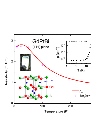
Our optical reflectivity measurements were conducted on a single crystal of lateral dimensions of mm2 with a shiny (111) surface (Fig. 1); the sample thickness was around 0.8 mm. Standard four-point dc-resistivity and Hall measurements, performed on a smaller piece (a Hall bar) cut from the specimen used for optics, indicated a semiconducting behavior with a well-known antiferromagnetic transition at 9 K Canfield1991 . Hall measurements show -type conduction and a very low carrier density of cm-3 at (cf. different samples from Ref. Hirschberger2016 ). All optical experiments reported here are made in the paramagnetic state ( K), where the Dirac physics of GdPtBi is primarily discussed Hirschberger2016 ; Liang2018 ; Kumar2017 ; Yang2017 .
Optical reflectivity was measured at 10 to 300 K over a frequency range from to cm-1 (2.5 meV – 2.73 eV) using two Fourier-transform infrared spectrometers. The spectra in the far-infrared ( cm-1) were recorded by a Bruker IFS 113v spectrometer. Here, an in-situ gold evaporation technique was utilized for reference measurements Homes1993 . At frequencies above 700 cm-1, a Bruker Hyperion microscope attached to a Bruker Vertex 80v spectrometer was used. Freshly evaporated gold mirrors served as references in this setup. Complex optical conductivity was obtained from using Kramers-Kronig transformations Dressel2002 . High-frequency extrapolations were made utilizing the x-ray atomic scattering functions Tanner2015 . At low frequencies, we used the same procedure as recently applied for materials with highly mobile carriers Schilling2017Yb ; Schilling2017Zr : we fitted the spectra with a set of Lorentzians fit and then used the results of these fits between and 20 cm-1 as zero-frequency extrapolations for subsequent Kramers-Kronig transformations.
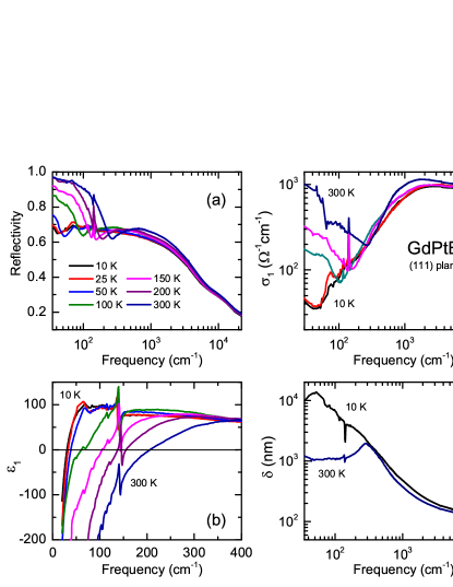
Figure 2 displays an overview of the results obtained in our optical investigations. Panel (a) shows the reflectivity for all measurement temperatures. Panels (b) and (c) represent (the real parts of) the dielectric constant and the optical conductivity , respectively. Finally, panel (d) demonstrates the skin depth of our sample at 10 and 300 K (curves for intermediate temperatures lie in between these ones). Important is that the skin depth exceeds 50 nm for all measured temperatures and frequencies. In the most interesting low-energy region, it is in the micrometer range. Hence, our optical measurements reflect bulk properties.
A sharp phonon peak is seen in all data sets at cm-1. Another phonon at cm-1 is weak, but resolvable, especially in [panel (b)]. The frequency positions of both phonon modes have only marginal temperature dependence. No other phonons are detected, in agreement with group analysis, which predicts two infrared-active optical modes for the half-Heusler structure phonons . All other features of the optical response are due to intra- or interband electronic transitions, as discussed below.
A temperature-dependent plasma edge dominates the low-energy part ( cm-1) of the reflectivity spectra [panel (a)]. The edge corresponds to the screened plasma frequency of free carriers, Dressel2002 , and is also seen in panel (b) as zero crossings of the curves. From the same panel, it can also be noted that the background dielectric constant is rather high, around 70 – 100. This leads to a low unscreened plasma frequency (for example, cm-1 at 10 K), in agreement with the low free-carrier concentration found in Hall measurements. The free-electron contribution to the optical conductivity [panel (c)] is seen as a Drude-like mode at the lowest frequencies. At lower temperatures, this mode narrows and loses its spectral weight in accordance with decreasing at . As K, only marginal traces of the free-carrier (intraband) contribution are seen in the recorded spectra: above cm-1, reflects only the interband optical transitions (and the phonons, as mentioned above).
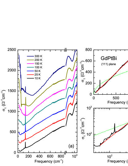
A striking feature of the optical conductivity is its almost perfect linearity in a broad range in the far infrared. This can be seen best in Fig. 3, where experimental conductivity is shown alongside linear fits [square-root behavior of conductivity, expected for parabolic bands, is also shown for comparison]. The behavior of experimental is basically the same for the three lowest measurement temperatures (10, 25, and 50 K): it linearly increases with in the spectral range from approximately 50 up to almost 800 cm-1. The observation of this linearity is an important result of this work. As discussed above, the linearity of the low-energy is a signature of 3D linear bands Hosur2012 ; Bacsi2013 ; Chen2015 ; Xu2016 ; Neubauer2016 ; Kimura2017 . However, other band structures may also provide similar . For example, it can be a cumulative effect of many bands with predominantly, but not exclusively, linear dispersion relations. Such a situation was recently reported by some of us for the Weyl semimetal NbP at somewhat higher frequencies Neubauer2018 . Wavy deviations from a perfectly linear increase of [see, Figs. 3(b) and 3(c)] indicate that a similar scenario might be realized in GdPtBi.
To get an insight into the origin of linear , we performed band-structure calculations and then computed the interband optical conductivity. In the calculations, we used the linear muffin-tin orbital method (LMTO) Andersen75 as implemented in the relativistic PY LMTO computer code APSY95 ; AHY04 . The Perdew-Burke-Ernzerhof GGA PBE96 was used for the exchange-correlation potential. The states of gadolinium were treated as semicore states. The spin polarization was not considered in order to model the paramagnetic state studied in this work ( K). Relativistic effects, including SOC, were accounted for by solving the four-component Dirac equation inside atomic spheres. BZ integrations were done using the improved tetrahedron method BJA94 .
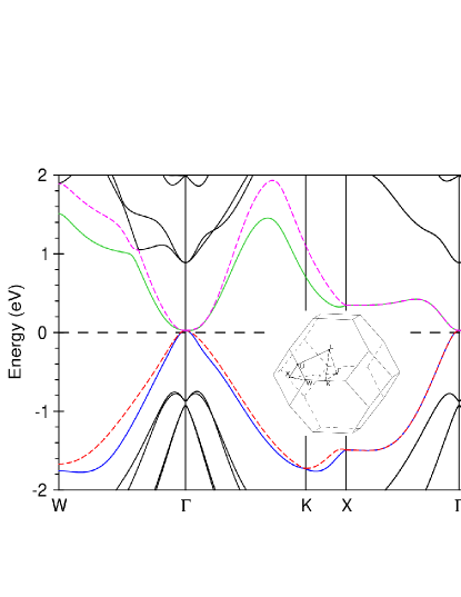
The calculated band structure is shown in Fig. 4. Our calculations confirm the presence of basically parabolic bands, touching each other at the point. A closer look at the low-energy band structure [Figs. 5(a) and 5(b)] reveals the presence of a triple point (marked as 3p in the figure) along the line, in agreement with previous calculations Yang2017 . The bands in the plane normal to the direction possess linear dispersion relations, as shown for the direction in panel (b). There are eight symmetry-equivalent triple points per BZ. The band structure of GdPtBi near these points is similar to a Weyl or Dirac semimetal with tilted cones, as seen best in panel (a).
Our calculations predict the triple points to be situated 18 meV below the Fermi level. However, the real GdPtBi crystals are known to often possess unintentional doping, which is impossible to control at the crystal-growing stage Hirschberger2016 . Thus, the position of the chemical potential can in reality be within a few tens of meV off the calculated value. It is instructive to note here that the linear-in-frequency is expected for tilted cones (of any type), if the chemical potential is situated at the node Carbotte2016 . In practice, ( is measured form the node hereafter) should be below the measurement frequency window. Such a situation can be relevant for our GdPtBi sample, as we discuss below. This is also in agreement with the very small free-carrier (Drude) contribution and low Hall carrier density.
The band structure of GdPtBi in the vicinity of the Fermi level is obviously more complex than the model band structure used in Ref. Carbotte2016 . Thus, as mentioned above, we compute from the obtained band structure. In these computations, the dipole matrix elements for interband optical transitions were calculated on a -mesh using LMTO wave functions – it is necessary to use sufficiently dense meshes in order to resolve transitions at low energies Chaudhuri2017 . The real part of the optical conductivity was calculated using the Kubo-Greenwood linear-response expressions WC74 with the BZ integration performed using the tetrahedron method.
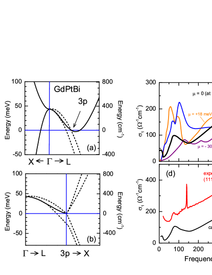
Before we discuss the results of these calculations, we would like to note that obtaining a good agreement between experimental and computed conductivity is known to be challenging Yu2010 ; Santos2018 . This is particularly the case for (topological) semimetals, where only a qualitative match can typically be achieved Neubauer2018 ; Grassano2018 ; Kimura2017 ; Frenzel2017 ; Chaudhuri2017 . In the relevant for this study low-energy part of the spectrum (below meV), a reasonable agreement is particularly hard to obtain Kimura2017 ; Chaudhuri2017 . Nevertheless, for GdPtBi we have reached a fairly good agreement between our calculations and the experimental spectra at low energies.
The results are shown in Figs. 5(c) and 5(d). Because of the possible carrier doping in GdPtBi, discussed above, we have some freedom in setting the position of the chemical potential. We varied within meV from the triple point and compared the computed spectra to each other and to the experiment. Panel (c) demonstrates that the best linear , extrapolating to 0 at , is obtained, if the chemical potential is at the triple point (). If we vary , the calculated either develops huge peaks at low energies ( cm-1), or does not extrapolate to 0 as , or both. Also, the quasilinear part of the conductivity, calculated for , spans over the largest frequency range. Thus, we choose the curve for further comparison with our experimental results; see panel (d). (Obviously, very small deviations from on a meV scale are possible.)
In Fig. 5(d), a low-temperature (25 K) experimental curve is shown alongside the calculated . The overall linear increase of the experimental curve is well reproduced. It is also evident that both the calculations and experiment provide some deviations from perfect linearity. Most remarkable is the bump, present in the calculations and experiment, at around 80 cm-1. Such deviations reflect the fact that the band structure is not ideally linear in all three directions but more complex. Overall, we can conclude that the observed interband optical conductivity in GdPtBi originates from the transitions between all the bands near the triple points. Linear terms dominate the dispersions of these bands in the close vicinity of the nodes, leading to the almost, but not perfectly, linear optical conductivity in GdPtBi at low frequencies.
From our band-structure calculations, we can compute the Fermi velocities for the crossing bands. Calculations exactly at the triple point are technically challenging, and, thus, we compute in a close vicinity of it along the line – at from the triple point; here is the lattice constant. For the doubly degenerate electronlike band, we obtain and m/s, while for the nondegenerate holelike band and m/s.
In a simple model of electron-hole symmetric crossing linear electronic bands, the optical conductivity is related to the Fermi velocity via Hosur2012 ; Bacsi2013 , where is the band degeneracy at the crossing point (e.g., a Dirac node has ) and is the number of nodes per BZ. Obviously, this simple formula has a very limited applicability. Nevertheless, if we straightforwardly apply it to our experimental and set and , we obtain an averaged Fermi velocity of m/s, which is in good agreement with the values calculated above.
In summary, we have found the low-frequency optical conductivity of GdPtBi to be linear in a broad frequency range (50 – 800 cm-1, 6 – 100 meV at K). This linearity strongly suggests the presence of three-dimensional linear electronic bands with band crossings near the chemical potential. A comparison of our data with the optical conductivity computed from the band structure demonstrates that the observed originates from the transitions near the triple points. From the optical spectra, we directly determine the plasma frequency of free carriers in GdPtBi and estimate an averaged Fermi velocity at the nodes: m/s. The values of , calculated from the band structure near the triple points along the line, range from to m/s depending on the band and the momentum direction.
We are grateful to Ece Uykur and Dominik Günther for valuable experimental support, to Gabriele Untereiner for technical assistance, and to Johannes Gooth for many fruitful discussions. This work was funded by DFG via grant No. DR228/51-1.
References
- (1) L. Wollmann, A. K. Nayak, S. S. P. Parkin, and C. Felser, Annu. Rev. Mater. Res. 47, 247 (2017).
- (2) K. Manna, Y. Sun, L. Müchler, J. Kübler, and C. Felser, Nat. Rev. Mater. 3 244 (2018).
- (3) F. Casper, T. Graf, S. Chadov, B. Balke, and C. Felser, Semicond. Sci. Technol. 27, 063001 (2012).
- (4) S. Chadov, X. Qi, J. Kübler, G. H. Fecher, C. Felser, and S. C. Zhang, Nat. Mater. 9, 541 (2010).
- (5) H. Lin, A. Wray, Y. Xia, S. Xu, S. Jia, R. J. Cava, A. Bansil, and M. Z. Hasan, Nat. Mater. 9, 546 (2010).
- (6) D. Xiao, Y. Yao, W. Feng, J. Wen, W. Zhu, X.-Q. Chen, G. M. Stocks, and Z. Zhang, Phys. Rev. Lett. 105, 096404 (2010).
- (7) W. Al-Sawai, H. Lin, R. S. Markiewicz, L. A. Wray, Y. Xia, S.-Y. Xu, M. Z. Hasan, and A. Bansil, Phys. Rev. B 82, 125208 (2010).
- (8) C. Liu, Y. Lee, T. Kondo, E. D. Mun, M. Caudle, B. N. Harmon, S. L. Bud’ko, P. C. Canfield, and A. Kaminski, Phys. Rev. B 83, 205133 (2011).
- (9) Z. K. Liu, L. X. Yang, S.-C. Wu, C. Shekhar, J. Jiang, H. F. Yang, Y. Zhang, S.-K. Mo, Z. Hussain, B. Yan, C. Felser, and Y. L. Chen, Nat. Commun. 7, 12924 (2016).
- (10) J. A. Logan, S. J. Patel, S. D. Harrington, C. M. Polley, B. D. Schultz, T. Balasubramanian, A. Janotti, A. Mikkelsen, and C. J. Palmstrøm, Nat. Commun. 7, 11993 (2016).
- (11) C. Shekhar, A. K. Nayak, S. Singh, N. Kumar, S.-C. Wu, Y. Zhang, A. C. Komarek, E. Kampert, Y. Skourski, J. Wosnitza, W. Schnelle, A. McCollam, U. Zeitler, J. Kübler, S. S. P. Parkin, B. Yan, and C. Felser, arXiv:1604.01641.
- (12) M. Hirschberger, S. Kushwaha, Z. Wang, Q. Gibson, S. Liang, C. A. Belvin, B. A. Bernevig, R. J. Cava, and N. P. Ong, Nat. Mater. 15 1161 (2016).
- (13) S. Liang, J. Lin, S. Kushwaha, J. Xing, N. Ni, R. J. Cava, and N. P. Ong, Phys. Rev. X 8, 031002 (2018).
- (14) N. Kumar, S. N. Guin, C. Felser, and C. Shekhar, Phys. Rev. B 98, 041103 (2018).
- (15) H. Yang, J. Yu, S. S. P. Parkin, C. Felser, C.-X. Liu, and B. Yan, Phys. Rev. Lett. 119, 136401 (2017).
- (16) Z. Zhu, G. W. Winkler, Q. S. Wu, J. Li, and A. A. Soluyanov, Phys. Rev. X 6, 031003 (2016).
- (17) M. Dressel and G. Grüner, Electrodynamics of Solids (Cambridge University Press, Cambridge, 2002).
- (18) T. Ando, Y. Zheng, and H. Suzuura, J. Phys. Soc. Jpn. 71, 1318 (2002).
- (19) P. Hosur, S. A. Parameswaran, and A. Vishwanath, Phys. Rev. Lett. 108, 046602 (2012).
- (20) A. Bácsi and A. Virosztek, Phys. Rev. B 87, 125425 (2013).
- (21) J. P. Carbotte, J. Phys. Condens. Matter 29, 045301 (2017).
- (22) S. P. Mukherjee and J. P. Carbotte, Phys. Rev. B 95, 214203 (2017).
- (23) S. Ahn, E. J. Mele, and H. Min, Phys. Rev. Lett. 119, 147402 (2017).
- (24) R. Y. Chen, S. J. Zhang, J. A. Schneeloch, C. Zhang, Q. Li, G. D. Gu, and N. L. Wang, Phys. Rev. B 92, 075107 (2015).
- (25) B. Xu, Y. M. Dai, L. X. Zhao, K. Wang, R. Yang, W. Zhang, J. Y. Liu, H. Xiao, G. F. Chen, A. J. Taylor, D. A. Yarotski, R. P. Prasankumar, and X. G. Qiu, Phys. Rev. B 93, 121110 (2016).
- (26) D. Neubauer, J. P. Carbotte, A. A. Nateprov, A. Löhle, M. Dressel, and A. V. Pronin, Phys. Rev. B 93, 121202 (2016).
- (27) S. I. Kimura, H. Yokoyama, H. Watanabe, J. Sichelschmidt, V. Süß, M. Schmidt, and C. Felser, Phys. Rev. B 96, 075119 (2017).
- (28) Y. Shao, Z. Sun, Y. Wang, C. Xu, R. Sankar, A. J. Breindel, C. Cao, M. M. Fogler, F. Chou, Z. Li, T. Timusk, M. B. Maple, and D. N. Basov, arXiv:1806.01996.
- (29) P. C. Canfield, J. D. Thompson, W. P. Beyermann, A. Lacerda, M. F. Hundley, E. Peterson, and Z. Fisk, J. Appl. Phys. 70, 5800 (1991).
- (30) C. C. Homes, M. Reedyk, D. A. Cradles, and T. Timusk, Appl. Opt. 32, 2976 (1993).
- (31) D. B. Tanner, Phys. Rev. B 91, 035123 (2015)
- (32) M. B. Schilling, A. Löhle, D. Neubauer, C. Shekhar, C. Felser, M. Dressel, and A. V. Pronin, Phys. Rev. B 95, 155201 (2017).
- (33) M. B. Schilling, L. M. Schoop, B. V. Lotsch, M. Dressel, and A. V. Pronin, Phys. Rev. Lett. 119, 187401 (2017).
- (34) Similar fitting procedures can, in principle, be utilized even as substitutes of the Kramers-Kronig analysis; see A. B. Kuzmenko, Rev. Sci. Instrum. 76, 083108 (2005) and G. Chanda, R. P. S. M. Lobo, E. Schachinger, J. Wosnitza, M. Naito, and A. V. Pronin, Phys. Rev. B 90, 024503 (2014).
- (35) Z. V. Popović, G. Kliche, R. Liu, and F. G. Aliev, Solid State Commun. 74, 829 (1990); P. Hermet, K. Niedziolka, and P. Jund, RSC Adv. 3, 22176 (2013); C. Çoban, K. Çolakoǧlu, and Y. Ö. Çiftçi, Phys. Scr. 90, 095701 (2015); D. Shrivastava and S. P. Sanyal, Physica C 544, 22 (2018).
- (36) D. Neubauer, A. Yaresko, W. Li, A. Löhle, R. Hübner, M. B. Schilling, C. Shekhar, C. Felser, M. Dressel, and A. V. Pronin, arXiv:1803.09708.
- (37) O. K. Andersen, Phys. Rev. B 12, 3060 (1975).
- (38) V. N. Antonov, A. Y. Perlov, A. P. Shpak, and A. N. Yaresko, J. Magn. Magn. Mater. 146, 205 (1995).
- (39) V. Antonov, B. Harmon, and A. Yaresko, Electronic structure and magneto-optical properties of solids (Kluwer Academic, Dordrecht, 2004).
- (40) J. P. Perdew, K. Burke and M. Ernzerhof, Phys. Rev. Lett. 77, 3865 (1996).
- (41) P. E. Blöchl, O. Jepsen, and O. K. Andersen, Phys. Rev. B 49, 16223 (1994).
- (42) J. P. Carbotte, Phys. Rev. B 94, 165111 (2016).
- (43) D. Chaudhuri, B. Cheng, A. Yaresko, Q. D. Gibson, R. J. Cava, and N. P. Armitage, Phys. Rev. B 96, 075151 (2017).
- (44) C. S. Wang and J. Callaway, Phys. Rev. B 9, 4897 (1974).
- (45) P. Y. Yu and M. Cardona, Fundamentals of Semiconductors: Physics and Materials Properties (Springer, Berlin, 2010).
- (46) D. Santos-Cottin, Y. Klein, Ph. Werner, T. Miyake, L. de’ Medici, A. Gauzzi, R. P. S. M. Lobo, and M. Casula, Phys. Rev. Mater. 2, 105001 (2018).
- (47) D. Grassano, O. Pulci, A. M. Conte, and F. Bechstedt, Sci. Rep. 8, 3534 (2018).
- (48) A. J. Frenzel, C. C. Homes, Q. D. Gibson, Y. M. Shao, K. W. Post, A. Charnukha, R. J. Cava, and D. N. Basov, Phys. Rev. B 95, 245140 (2017).