Conductance relaxation in GeBiTe - slow thermalization in an open quantum system.
Abstract
This work describes the microstructure and transport properties of GeBiTe films with emphasis on their out-of-equilibrium behavior. Persistent-photoconductivity (PPC), previously studied in the phase-change compound GeSbTe is also quite prominent in this system. Much weaker PPC response is observed in the pure GeTe compound and when alloying GeTe with either In or Mn. Films made from these compounds share the same crystallographic structure, the same p-type conductivity, a similar compositional disorder extending over mesoscopic scales, and similar mosaic morphology. The enhanced photo-conductive response exhibited by the Sb and Bi alloys may therefore be related to their common chemistry. Persistent-photoconductivity is observable in GeBiTe films at the entire range of sheet resistances studied in this work (10 to 55M). The excess conductance produced by a brief exposure to infrared illumination decays with time as a stretched-exponential (Kohlrausch law). Intrinsic electron-glass effects on the other hand, are observable in thin films of GeBiTe only for samples that are strongly-localized just like it was noted with the seven electron-glasses previously studied. These include a memory-dip which is the defining attribute of the phenomenon. The memory-dip in GeBiTe is the widest amongst the germanium-telluride alloys studied to date consistent with the high carrier-concentration N10cm of this compound. The thermalization process exhibited in either, the PPC-state or in the electron-glass regime is sluggish but the temporal law of the relaxation from the out-of-equilibrium state is distinctly different. Coexistence of the two phenomena give rise to some non-trivial effects, in particular, the visibility of the memory-dip is enhanced in the PPC-state. The relation between this effect and the dependence of the memory-effect magnitude on the ratio between the interparticle-interaction and quench-disorder is discussed.
pacs:
72.20.-i 72.40.+w 78.47.da 72.80.NgI Introduction
The approach to equilibrium of quantum systems is a fundamental problem that has received wide theoretical attention, mostly in close systems 1 ; 2 . Thermalization of open systems is a less researched subject although it is relevant for most naturally occurring processes. This is the case for out-of-equilibrium electronic transport in solids where coupling to a heat-bath via phonons usually plays a role at any finite temperature. In metals and semiconductors the rate of electron-phonon (e-ph) inelastic scattering may be appreciable; even at sub-Kelvin temperatures is typically 10-10s at 1K 3 . An efficient e-ph coupling is the main reason for the fast relaxation of the electronic system after it has been taken out of equilibrium by a light-pulse or by Joule-heating it.
There are however situations where electronic relaxation is a sluggish process despite the presence of phonons; persistent photoconductivity (PPC), and the relaxation exhibited by electron-glasses are examples for such cases. In both phenomena the electronic conductance G is enhanced in their out of the equilibrium state, and in both the relaxation of G from the excited state may be a very slow process that may be monitored over time scales that are many orders of magnitude longer than phonon relaxation times. The slow relaxation associated with these phenomena make systems that exhibit them prime candidates for experimentally studying thermalization in open quantum systems.
PPC has been observed in lightly-doped semiconductors with carrier-concentration N typically smaller than 10cm 4 ; 5 ; 6 ; 7 ; 8 . Recently this phenomenon was observed in GeSbTe alloys, p-type degenerate semiconductors with N 10cm9 . When Anderson localized, samples of GeSbTe exhibited both intrinsic 10 electron-glass effects and PPC. The interplay of the two coexisting phenomena showed non-trivial effects 10 ; 11 .
In this work we discuss attempts to obtain similar results for other systems based on GeTe by incorporating either In, Mn, or Bi as the third element in the alloy. Despite the high concentration of these chemically different foreign elements, the resulting ternary compounds shared the same crystallographic structure and p-type conductivity of the GeTe parent compound. On the other hand, the transport properties differed markedly among the produced alloys, in particular in terms of their PPC performance. Incorporating In or Mn atoms in the GeTe matrix did not seem to affect the PPC of the pure compound. Bismuth however, proved to give enhanced PPC effects similar to the behavior of the phase-changed material GeSbTe 10 . In addition, GeBiTe samples appear to be an efficient system for studying transport effects associated with the interplay between disorder and interactions: The material is easy to fabricate, it is flexible in terms of being able to vary its disorder over a wide range including driving it insulating without making it granular. The bulk of the work described below is mostly devoted to the results obtained with this system.
The persistent photo-conductivity and electron-glass features may be separately observed in GeBiTe samples and exhibit their distinct relaxation laws. When these phenomena coexist, on the other hand, the electron-glass features may be significantly modified, in particular, the memory-dip seems to have a larger magnitude in the PPC-state. It is argued that the ratio between the quench-disorder and inter-particle interaction plays a role in the visibility of the memory-dip. All other things being equal, this ratio is larger when the carrier-concentration N of the electron-glass is higher, which consistently results in a smaller magnitude of the memory-dip. However, in the PPC-state the interparticle-interaction to disorder ratio actually increases relative to the dark-state thus, in turn, enhancing the memory-dip magnitude.
Details of sample preparation, characterization, and their various measurements techniques are described in the next section. The results and their discussion are given in section III.
II Experimental
II.1 Sample preparation and characterization
Samples used in this study were prepared by co-depositing GeTe and either Bi, In, or Mn on room temperature substrates in a high-vacuum system (base pressure 0.8-1x10mbar). The GeTe (Equipment Support Company, USA) was e-gun deposited with rates of 0.6-1Å/second while Bi, In, or Mn were evaporated from a Knudsen source with a rate chosen such that the alloy composition should be close to 1:1:1. Film thickness varied in the range 40-60Å for the films measured in this work. Lateral dimensions of the samples used for transport measurements were 0.3-0.5mm long and 0.5mm wide.
Two types of substrates were used; 1mm-thick microscope glass-slides, and 1m SiO layer thermally grown on 100 silicon wafers. The Si wafers (boron-doped with bulk resistivity 2x10cm) were employed as the gate electrode in the field-effect measurements. The microscope glass-slides were mostly used for Hall-Effect measurements performed at room-temperatures. Theses revealed p-type carrier-concentration N in all these alloys. For the GeBiTe films, that were the main system used in this work, N varied in the range of (6-9)x10cm.
Each deposition batch included samples for transport measurements, samples for Hall-effect measurements, and samples for structural and chemical analysis. For the latter study, carbon-coated Cu grids were put close to the sample during its deposition. These grids received the same post-treatment as the samples used for transport measurements.
Transmission-electron-microscopy (TEM), using the Philips Tecnai G2) were employed to characterize the films composition and microstructure.
Polycrystalline samples of Ge(M)Te (where M stands for either Bi, In, or Mn) were obtained by mounting the as-deposited (amorphous) films on a hot-plate set to a temperature T=4705K for 2 minutes during which the sample was crystallized.
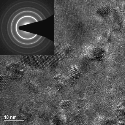
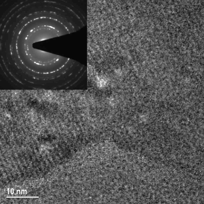
A TEM micrograph and associated diffraction pattern of typical GeBiTe and GeMnTe films produced in the above manner are shown in Fig.1 and Fig.2 respectively. These TEM micrographs and diffraction patterns illustrate the polycrystalline nature of the films and a tight, space-filling packing of the crystallites. The main difference between the Bi and the Mn alloys is obviously their different grain-sizes. These are just few nanometers for the GeBiTe film as compared with 100nm for GeMnTe. Similar grain-sizes were observed in our GeInTe films. The large disparity in grain-size is also reflected in the diffraction patterns (Fig.1 and Fig.2). Diffraction patterns taken from these films were consistent with the rhombohedral (R-3m) phase of GeTe in all samples made of the three ternary compounds.
Several types of structural defects may be observed in these micrograph; grain boundaries and twinning being the most prevalent. These defects, as well as the compositional-disorder (discussed next), and surface scattering are presumably responsible for restricting the mobility of the films.
The main difference between the GeBiTe and the GeMnTe and GeInTe films is their mobility. For the thickness range of 40-60Å, the GeBiTe samples had sheet resistance R□ in the range 2k-55M at 4K. With this range it was possible to cover a large part of the strongly-localized regime (R□h/e) which is a pre-requirement for observing inherent electron-glass effects 12 . In contrast, we were not yet able to push R□ much above 10k in samples made from either of the two other alloys even by deliberate surface-oxidation. This is presumably the reason for our failure to detect electron-glass effects in GeMnTe and GeInTe films. The higher resistance obtainable in the GeBiTe alloy may be in part due to their much smaller grain-size as noted above. However, the grain-size in the previously studied GeSbTe 10 was even larger than in GeMnTe and GeInTe and had more pronounced texture (which means less boundary scattering) than that observed in GeMnTe while films with R□ 50M were easily produced even in thicker films 10 . Inter-grain scattering is therefore not likely to be the main source of disorder in these alloys.
The focus of this work is the difference between the two mechanisms for slow relaxation and therefore, in the following, data are shown mainly for the GeBiTe samples where both PPC and electron-glass effects are observable.
The stoichiometry of the GeBiTe films was measured by EDS (Energy Dispersive Spectroscopy) attachment of the TEM. Different preparation runs produced films that usually had the average stoichiometry close to the desired goal mentioned above. However, there was noticeable composition heterogeneity on a mesoscopic spatial scale. This kind of disorder is quite common in alloys and may be accompanied by spatial fluctuations in carrier-concentration 13 . A similar composition heterogeneity has been seen also in GeTe 14 . Figure 3 shows the distribution of local stoichiometry (on a mesoscopic 40nm scale) across a typical GeBiTe film.
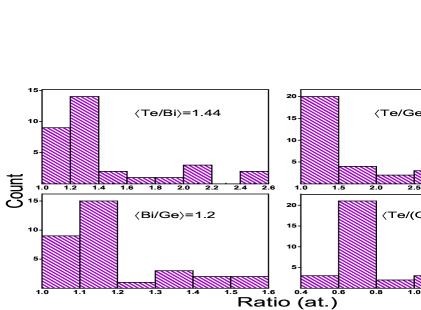
Composition variations may be accompanied by local variations of the carrier-concentration, and these are of particular importance in superconducting materials which are notoriously sensitive to the value of N. In the presence of disorder such inhomogeneities may lead to the appearance of superconducting islands embedded in an insulating matrix making it effectively a granular system 13 . One should be aware of these non-uniform structural aspects whenever the transport property one measures has a spatial scale that is smaller or comparable with the scale of the inhomogeneities.
II.2 Measurement techniques
Conductivity of the samples was measured using a two-terminal ac technique employing a 1211-ITHACO current preamplifier and a PAR-124A lock-in amplifier. Most measurements were performed with the samples immersed in liquid helium at T4.1K held by a 100 liters storage-dewar. This allowed up to two months measurements on a given sample while keeping it cold (and in the dark). These conditions are essential for measurements where extended times of relaxation processes are required at a constant temperature.
The gate-sample voltage (to be referred to as V in this work) in the field-effect measurements was controlled by the potential difference across a 10F capacitor charged with a constant current. The range of V used in this study reached in some cases 40V which is equivalent to the 20V used in previous work 15 where the gate-sample separation was 0.5m of as compared with the 1m SiO spacer used here.
The ac voltage bias in conductivity measurements was small enough to ensure near-ohmic conditions (except for the current-voltage plots). Optical excitations in this work were accomplished by exposing the sample to an AlGaAs diode operating at 0.880.05m mounted on the sample-stage 10-15mm from the sample. The diode was energized by a computer-controlled Keithley 220 current-source.
III Results and discussion
III.1 Field-effect measurements
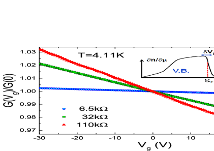
Conductance versus gate-voltage G(V) traces typical for diffusive GeBiTe samples are shown in Fig.4. The sign of G(V)/V that characterize the field-effect of these weakly-disordered samples is consistent with band-structure calculations for GeTe and similar compounds 16 . These theoretical models account for the p-type conduction in the material, in agreement with the sign of the Hall-Effect mentioned above. The Fermi-energy in this scenario appears at the top of the valence-band (see inset to Fig.4). Sweeping V changes the position of the Fermi-energy and the associated change in the conductance reflects the energy dependence of n, the thermodynamic density-of-states (DOS). The measured G(V) is a convoluted outcome of n() and D() - the energy-dependent diffusion-constant. For all GeBiTe samples reported here, D/0 and is larger with larger R□ as evidenced by the temperature dependence of their resistance; the resistance ratio R(4K)/R(300K) is: 1.23, 2.37, and 3.43 for the films with R□=6.5k, 32k, and 110k in Fig.4 respectively. This explains the reason for the a general trend in the field-effect data of disordered conductors; G(V)/V is a monotonously increasing function of R□.
Another feature appears in the G(V) traces of GeBiTe samples that have large enough disorder. This usually requires that the sheet-resistance of the films R□ be considerably larger than h/e25k. Figure 5 shows G(V) for a 50M film that was taken under the same conditions (temperature, sweep-rate) as the samples in Fig.4. The new feature is a local depression of G(V) centered, in this case, at V=0V. This feature is the memory-dip, a characteristic signature of the electron-glass 17 ; 18 ; 19 ; 20 ; 21 . It is believed to be a modulation of g(), the single-particle DOS resulting from inter-particle correlations 22 ; 23 ; 24 ; 25 .

A modulation of g() due to correlation effects occurs in disordered conductors even in the diffusive regime where field-effect measurements would reveal just the thermodynamic component n. The contribution of a single-particle DOS may be reflected in tunneling or photo-emission processes but it is not expected to show up in a thermodynamic measurement such as field-effect 26 . This however is because V is usually swept sufficiently slow to allow the electronic system to be in equilibrium. When the equilibration time of the system becomes longer than the inverse sweep-rate (a condition that is met in the electron-glass regime of highly disordered Anderson insulators 27 ), the underlying g() would manifest itself in the G(V) plot. The shape of this modulation, and its dependence on temperature, have been discussed by Lebanon, and Müller 23 . The magnitude of the memory-dip (defined in Fig.5), that will be referred to in this paper as ‘visibility’, depends therefore on how fast the gate-voltage is sweet. This was demonstrated in field-effect experiments on crystalline indium-oxide 12 . The slope of the thermodynamic component of G(V), on the other hand, is independent of V/t 12 .
The relative magnitude of the memory-dip G/G, increases with R□ as illustrated in Fig.6 for the GeBiTe films studied in this work. The average slope of G(V) for this samples is plotted on the same graph for comparison.
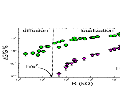
The qualitative features of these data are remarkably similar to those obtained on the half-a-dozen previously studied electron glasses 27 . In particular, they all show fast decline of the memory-dip magnitude as the diffusive regime is approached from the strongly-localized side, and a similar functional dependence of G/G on R□. This re-enforces the conclusion that strong-localization is a pre-requisite for observing electron-glass effects.
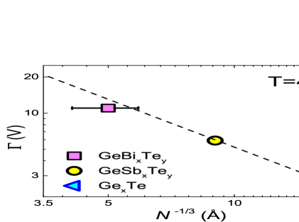
Another feature that appears to be common to electron-glasses is the dependence of their memory-dip width on the carrier-concentration N. A comparison of the memory-dip width and the carrier-concentration for the three germanium-telluride compounds studied to date is given in Fig.7. This shows a monotonous increase of with the inter-particle separation N. A similar dependence was found in the early work on amorphous indium-oxide 28 which hitherto was the only system where (N) was studied over a meaningful range of N. It would be interesting to be able to extend the range of the carrier-concentration in the GeTe system towards lower N values to see whether the relaxation time becomes very short below a certain concentration as it does in InO 28 .
Quantitatively however there are some features that distinguish the GeBiTe samples from previously studied electron-glasses. In particular, the magnitude of the memory-dip G/G is relatively small when compared with the magnitude of the slope of the thermodynamic density-of-states n for a given R□ (Fig.6). This is mainly due to the steep dependence of n on energy of this material. This makes it harder to observe the memory-dip in the G(V) traces than in e.g., beryllium 29 that has a similar magnitude of G/G for the same R□. The latter is still considerably smaller than exhibited by electron-glasses with lower carrier-concentrations N, InO and InO (with N10cm), a point that will be addressed later in this paper.
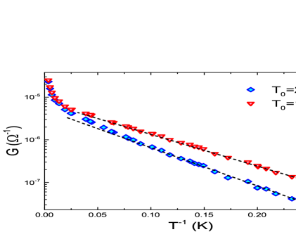
As is clear from Fig.6, a memory-dip could be observed only in strongly insulating samples. The conductance G of these samples, like all other electron-glasses, exhibit exponential temperature dependence of conductivity. Temperature dependence of G is shown in Fig.8 for two of the studied GeBiTe samples.
It is interesting to compare these G(T) with the respective data of another electron-glass, InO which has structural features that are similar to GeBiTe. Both show a mosaic, polycrystalline structure. Insulating InOfilms with comparable value of R□ exhibit a behavior consistent with Mott-type hopping in two-dimensions; G(T)exp[-(T/T)] 30 rather than the simple activation G(T)exp[-T/T] shown by GeBiTe over the same temperature range (Fig.8). As noted above, a pre-condition for showing electron-glass properties is strong-localization, and one of the characteristic features of this state is an exponential G(T). However, the specific form of this function, and the structural details of the system appear to be unimportant. In other words, the features of electron-glasses may not be identified by the specific form their G(T) takes. An exponential G(T) whether simple activation or of the stretched-exponential kind is a necessary condition but, for observing the memory-dip in field-effect measurement other requirements have to be met, in particular strong disorder 27 .
GeBiTe and InO differ also in their sensitivity to applied electric fields; non-ohmicity in hopping systems often sets in at rather small fields at liquid helium temperatures 31 ; 32 ; 33 ; 34 and the present system is no exception; R□ as function of the applied voltage V are plotted in Fig.9 for four GeBiTe samples with different degrees of disorder clearly show the common trend.
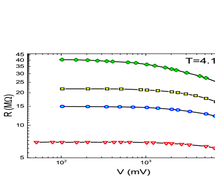
Susceptibility to non-ohmic behavior is more conspicuous in InO than in the GeBiTe films: To illustrate, InO sample with R□=12.5M decreased by 90% upon applying a field of 10V/cm at T=4.1K 37 while under the same conditions the drop of R□ is a mere 2.4% for the GeBiTe film with R□=15M (Fig.9).
Non-ohmicity deep in the hopping regime is mainly caused by a field-assisted mechanism 31 ; 32 ; 33 ; 34 but Joule-heating is an accompanying factor; for a given applied field the relative importance of heating would become larger when the resistance is smaller. The higher sensitivity of InO to the applied field is related to the compounded effect of both mechanisms. As a low N system the hopping-length for a given temperature and resistance is likely longer than in the GeBiTe system which makes the field-assisted mechanism stronger for a comparable field strength. The heating sensitivity of the conductance involves (among other things) the electron-phonon inelastic-scattering rate. This is likely to be more important in InO due to its unusually large Debye temperature 36 . In any case, the larger range of applied voltages over which linear-response condition may be maintained using GeBiTe samples should be a convenient feature for experimental study of hopping conductivity.
There is another feature of GeBiTe that may make it a versatile test-bed for a variety of non-equilibrium phenomena; GeBiTe films exhibit pronounced response to photo-excitation. Just like it was observed in GeSbTe films 9 ; 11 , exposure to infrared illumination increased the samples conductance by a certain G which persisted long after the light source was turned off. The experimental protocol used for optical excitation is illustrated in Fig.10. The experiment typically begins 24 hours after the sample is cooled-down to 4.1K by recording G(t) for 1-2 minutes to establish a baseline, near-equilibrium conductance G0. The IR source was then turned on for 3 seconds and then turned off while G(t) continues to be measured.
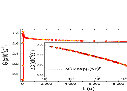
The figure depicts the conductance dependence during excitation and the ensuing relaxation following its termination. The latter has a characteristic time dependence that fits a stretched-exponent law:
| (1) |
(see inset to Fig.10). This is a manifestation of persistent photoconductivity (PPC), a phenomenon that has been frequently observed in many semiconductors 3 ; 4 ; 5 ; 6 ; 7 ; 8 and recently found in the compound GeSbTe 9 ; 11 .
In general, the relative change of the conductance due to the brief infrared exposure G/G increases with R□ as shown in Fig.11.
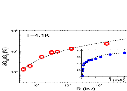
The same energy-flux (1mA current through the infrared diode for 3s) was delivered to all samples in the series with sheet-resistances of 4k to 55M. This value was chosen after studying the dependence of the effect on the excitation current shown in the inset to Fig.11. The excitation by 1mA was chosen as a compromise between achieving an appreciable G while minimizing heating and associated detrimental effects to the electron-glass state which may coexist with the PPC when the system is in the strongly-localized regime.
The detailed behavior of the PPC in the GeBiTe films turns out to be similar to that of GeSbTe 9 ; 11 ; in both systems PPC is observable in samples that are in the diffusive regime as well as in strongly-localized samples. The relaxation law associated with PPC is essentially the same for a diffusive sample (Fig.12) and for a strongly-localized sample (Fig.13). The latter is in the electron-glass phase and exhibits a well-developed memory-dip whereas the G(V) the diffusive sample reveal only the thermodynamic DOS in the field-effect scan.
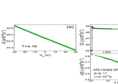
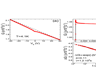
These two alloys are also similar in terms of magnitude and fit parameters to the stretched exponential relaxation law. The G(t) measured following the infrared excitation of the samples shown in Fig.11 could be fitted to Eq.1 with the same =0.110.005 as a best-fit parameter. The other fit parameter in the stretched-exponential law is that is found to be of order 10 to 10 in all our samples. There was no systematic dependence of on the sample sheet resistance R□. Similar values for and the relaxation-time were found at these temperatures in the relaxation law of PPC in AlGaAs compounds 5 and in the GeSbTe films studied previously 9 ; 11 .
Applying the infrared protocol to GeMnTe and GeInTe samples resulted in a considerably lower G/G values as compared with GeSbTe and the GeMnTe samples with similar resistances. A comparison between the response of GeMnTe and GeInTe samples with GeBiTe films is shown in Fig.14.
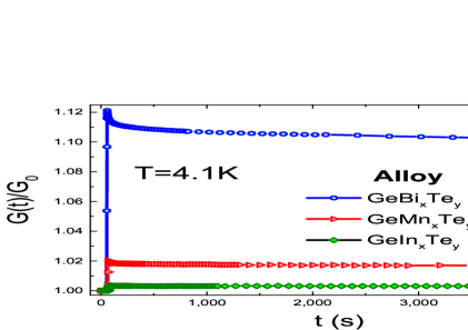
The G(t) plots of the infrared protocol for these samples plotted in Fig.14 are the highest in terms of the magnitude of G obtained so far. The overall appearance of these relaxation curves appear to be similar to those of the GeBiTe and GeSbTe alloys but the signal-to-noise of the G(t) data are not yet good enough to allow for a reliable determination of and for either GeMnTe or GeInTe. In addition, there were appreciable fluctuations in the magnitude of G/G taken from different preparation batches of these alloys. This may indicate that the PPC in GeMnTe and GeInTe (as well as in the parent compound GeTe) results from the spurious occurrence of a defect and that the enhanced PPC response in the GeBiTe and GeSbTe is due to a catalytic effect of incorporating Bi or Sb in the ternary alloy.
Our persistent-photoconductivity results in these GeTe alloys resembles in many aspects the behavior reported in compounds based on PbTe, a system that has been extensively studied 4 . In particular, the sensitivity of the PPC magnitude to the specific chemistry of the element added to the alloy seems to be a common feature (the dopants that yield higher PPC efficiency are however different).
The similar dynamics of the GeBiTe and the GeSbTe alloys in their PPC-state may be an important clue for unraveling the nature of the defect responsible for the long-lived PPC state. While the involvement of a massive defect is believed to be a key element in most models for the PPC phenomenon 4 , the basic question is whether the relevant defect is the added element itself (Sb or Bi in our case) or it is an indirect result of its presence in the alloy 4 . Given the substantial difference in the masses of Sb and Bi, one would argue that the similar parameters of the relaxation dynamics in the PPC-state of GeBiTe and GeSbTe as well as the similar behavior of the undoped GeTe, favor the indirect scenario.
III.2 Modification of the electron-glass behavior in the PPC state
Strongly-localized samples of GeBiTe exhibit all the qualitative nonequilibrium features found in previously studied electron-glasses. These are distinguishable from the PPC observed in this system in a number of aspects. First and foremost, as mentioned above, unlike persistent photoconductivity, the electron-glass features are not observed in the diffusive regime of the system. Secondly, there are more ways to take the electron-glass far from the equilibrium than just by exposure to electromagnetic radiation; stressing the sample with longitudinal field 38 , and changing the density of carriers in the system (via a change of the gate-voltage), are two examples for unique ways to take the system away from equilibrium. Finally, the relaxation-law towards equilibrium of the conductance is logarithmic with time for the electron-glass as compared with the stretched-exponential law for PPC. Figure 15 illustrates two of the above distinguishing features of the electron-glass.
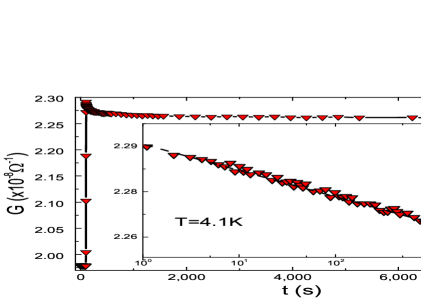
Some electron-glass features are significantly modified when coexisting with persistent photoconductivity. This is not surprising; the ”persistent” mode is not a stationary-state, the concentration of charge-carriers continuously diminishes with time, and this has consequences. It is easy to understand that in the PPC-state the relaxation law of the electron-glass would appear different because the background conductivity is decaying with a stretched-exponential law. Figure 16 demonstrates such a case using the gate-protocol to drive the electron-glass away from ”equilibrium” while the system is still relaxing from the infrared exposure applied several hours before.
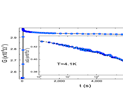
The main effect of the combined relaxation in this case is a modified relaxation-law that deviates from the log(t) dependence that characterizes the electron-glass. The total change of G observed during the 7,000 seconds, over which data are plotted in Fig.16, is comparable in magnitude to the sum of the respective G’s estimated from the relaxations due to the PPC and the electron-glass (assuming that each is present without the other). This assumption however cannot be accurate; coexistence of the two nonequilibrium phenomena manifestly produces effects that are not consistent with simple superposition. This is demonstrated in the experiment described in Fig.17. The figure compares G(V) for a GeBiTe film before and after being exposed to the infrared source yielding. a counter-intuitive result: The sample under the PPC-state exhibits a larger amplitude of the memory-dip than the same film in its ”dark” state.
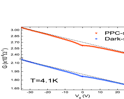
This is not a trivial result; it is natural to expect that exposing the electron-glass to infrared radiation would result in a diminishment of the memory-dip magnitude. In fact, it has been shown that above a certain threshold of energy-flux, infrared illumination may completely erase the memory-dip 39 . The energy flux associated with initiating the PPC-state is much smaller than used in 39 but the enhancement of the memory-dip is still an unexpected result.
A similar effect in GeSbTe was ascribed to the presence of a series-resistor that is reduced in the PPC-state 9 ; 11 . This was motivated by the observation of the concomitant increase of the slope of n(). However, this approach was not able to account for the magnitude of the enhancement. Besides, the lack of change in the slope of the thermodynamic DOS in the present case [see Fig.17], makes this line of explanation questionable anyhow (although, given the inhomogeneous structure, part of the effect might be related to reduction of a series resistor).
An alternative scenario to account for the enhanced memory-dip is based on the observation that the interaction-to-disorder ratio plays a role in the magnitude of the memory-dip and on the realization that this ratio increases in the PPC-state relative to the dark-state.
That the visibility of the memory-dip is a function of the ratio of Coulomb-interaction I to disorder W should be clear; recall that this modulation in G(V) has it roots in the competition between interaction and disorder: The memory-dip vanishes when disorder is small, and it is obviously absent altogether when interaction is turned-off. It is then intuitively expected that the memory-dip is most conspicuous when the disorder and interaction are comparable in magnitude.
The first point we wish to make here is that, over the range of parameters relevant for all the electron-glasses studied to date, IW.
The magnitude of the interparticle Coulomb interaction I for a system with a given N can be expressed by:
| (2) |
where is the dielectric constant of the medium and N is the interparticle average spacing. The disorder required to make the system strongly-localized (the pre-condition for being in the electron-glass phase 27 ) :
| (3) |
and using free-electron formula this may be cast in terms of carrier-concentration:
| (4) |
Note that all currently known electron-glasses have carrier-concentration in the range 2x10cmN5x10cm. As explained in 27 , systems with higher carrier-concentration than N10cm are difficult to strongly-localize unless by making granular, and the disorder in systems with N10cm is too weak to reduce transition rates sufficiently as to afford observation of the memory-dip (this is the reason for the failure of lightly-doped semiconductors to exhibit a memory-dip 27 ).
The values for W and I may now be estimated using Eq.2 and Eq.4 with the parameters for indium-oxide which has been studied over the widest range of carrier-concentration among all electron-glasses. Taking the dielectric constant as =10, and effective mass m*=0.3m one gets: I/W0.14 and I/W0.025 for InO samples with N4x10cm and N5x10cm respectively. These represent the two extreme limits in N over which electron-glasses were studied. The memory-dips associated with these limit-N values are plotted in Fig.18 illustrating the much larger G/G exhibited by the sample with the larger I/W ratio.
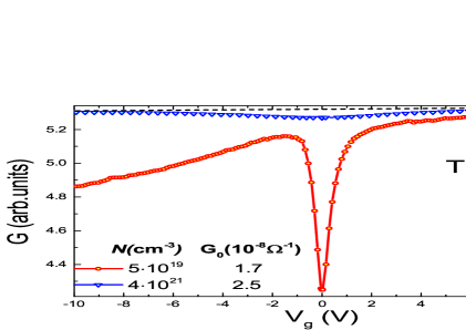
With these parameters for InO, the interaction-to-disorder ratio I/W1 would be obtained for an Anderson insulator with carrier-concentration N3x10cm. This N is well below the concentration where the relaxation time becomes too short for observation of electron-glass features by standard field-effect techniques. Note that it is the system with the lower N that has the larger I/W (and consequently larger G/G). This is so because IN while for electron-glasses WN, thus I/W actually decreases with N. In other words, all other things being equal, higher carrier-density means stronger Coulomb interaction but even stronger disorder.
Large values for G/G, of the order of 15-30% (for R□ 10M at 4K), are routinely obtained using the crystalline version of indium-oxide (InO) that also has low carrier-concentration N4x10cm 12 . On the other hand, electron-glasses with N 10cm typically show G/G of the order of 1% in samples with comparable R□. This is manifestly the case for the GeBiTe films studied here (see Fig.6 above).
The larger G observed in the PPC-state in both GeBiTe and the GeSbTe alloys may just be another example of the dependence of the memory-dip magnitude on I/W. Note that the enhanced conductivity in the PPC-state is mainly due to higher concentration of carriers N created by the optical excitation. Being in the strongly-localized regime, the system lacks metallic screening and therefore higher N means an increase in the interparticle-interaction I. It is less clear what, if any, is the accompanying change of disorder; The defect that hinders recombination in the PPC-state is presumed to be stabilized by a spatial-shift x of an atom, and possibly a change in the local charge 8 . The atomic displacement x, is sub-atomic 8 and thus much smaller than the localization-length which can hardly affect the perceived ionic-disorder. The scattering cross-section may however be different due to a change in the local charge in the PPC-state, but this may go either way. It is then plausible to assume that, in the PPC-state, the ratio of Coulomb-interaction to disorder is larger than in the dark-state. In that case the enhanced G/G in the PPC-state just follows a trend generally obeyed by all electron-glasses with N3x10cm.
To summarize, we presented in this paper experimental results that demonstrate coexistence of persistent-photoconductivity and electron-glass features in the degenerate semiconductor GeBiTe. Both phenomena exhibit sluggish conductance relaxation albeit due to different mechanisms. The conductance in the persistent-state is associated with the recombination of optically-generated excess charge. The process is slow presumably due to an energy-gap induced by a local structure re-arrangement. The different PPC susceptibility of the system to the nature of the element added to the alloy may help in identifying the microscopic mechanism involved.
The electron-glass dynamics, on the other hand, is associated with a change in the carriers mobility rather than carrier-concentration, and it is controlled by the combined effects of quench-disorder and variety of interaction-related mechanisms: Many-body effects, and several variations of the orthogonality-catastrophe 40 ; 41 ; 42 may further extend relaxation times. These phenomena demonstrate the richness and complexity of electronic transport in disordered and interacting quantum systems. The current study re-affirms the notion that electron-glasses with long relaxation times are inherent property of Anderson insulators where disorder is much larger than the Coulomb interaction.
The enhancement of the memory-dip magnitude induced by infrared radiation lead us to the conjecture that this feature of the electron-glass is controlled by the ratio of interaction and disorder. This was shown to be consistent with a number of experiments. Further experimental work needs to be done to test this trend in different materials. The magnitude G/G of the memory-dip is a more complicated issue to characterize than the width . At a given temperature, depends only on carrier-concentration of the system 12 . The magnitude of the memory-dip, on the other hand, depends on many other factors; G/G depends on the rate of sweeping the gate-voltage V, it depends on the time the sample equilibrated under V (history), and it depends on the R□ and on the sample thickness. In addition it may vary between different preparation batches (which suggest influence of structural details). The functional dependence of G/G on carrier-concentration is therefore not yet established. Nevertheless, the overall trend that G/G increases when the carrier-concentration decreases (in the regime IW) is clear enough. Some insight on this issue may come from numerical simulations looking at how the I/W ratio affects the memory-dip magnitude using the method of Meroz et al 25 ; in principle using this technique should allow probing the regime where the interaction is larger than the disorder, which is hard to implement experimentally.
Acknowledgements.
Illuminating discussions with Ady Vaknin on the electron-glass dynamics and with Dmitry Khokhlov on persistent-photoconductivity are gratefully acknowledged. This research has been supported by a grant No 1030/16 administered by the Israel Academy for Sciences and Humanities.References
- (1) Marcos Rigol1, Vanja Dunjko, and Maxim Olshanii, Nature, 452, 854 (2008).
- (2) Anatoli Polkovnikov, Krishnendu Sengupta, Alessandro Silva, and Mukund Vengalattore, Rev. Mod. Phys. 83, 863 (2011).
- (3) N. G. Ptitsina, G. M. Chulkova, K. S. Il’in, A. V. Sergeev, F. S. Pochinkov, E. M. Gershenzon, and M. E. Gershenson, Phys. Rev. B 56, 10089 (1997).
- (4) B. A. Akimova,. V. Dmitriev., R. Khokhlov, L. I. Ryabova, phys. stat. sol. (a) 137, 9 (1993).
- (5) T. Y. Lin, H. M. Chen, M. S. Tsai, and Y. F. Chen, F. F. Fang, C. F. Lin and G. C. Chi, Phys. Rev. B 58, 13793 (1998).
- (6) H. J. Queisser and D. E. Theodorou, Phys. Rev. Lett., 43, 401 (1979); Jennifer Misuraca, Jelena Trbovic, Jun Lu, Jianhua Zhao, Yuzo Ohno, Hideo Ohno, Peng Xiong, and Stephan von Molnár, Phys. Rev. B 82, 125202, (2010).
- (7) P. M. Mooney, Journal of Applied Physics 67, R1 (1990); Z. Su and J. W. Farmer, Appl. Phys. Lett. 59 , 30 (1991); D. Jia, J. Zhu, and B. Wu, Journal of The Electrochemical Society, 147 (1) 386 (2000).
- (8) D. V. Lang and R. A. Logan, Phys. Rev. Lett., 39, 635 (1977); D. V. Lang, R. A. Logan, and M. Jaros, Phys. Rev. B 19, 1015 (1979). The notion of a gap created by an atom-shift, which is central to the model, was first used by R. W. Gurney and N. F. Mott, in Trans. Faraday SOC. 35, 69 (1939).
- (9) Z. Ovadyahu , Phys. Rev. B. 91, 094204 (2015).
- (10) By ”intrinsic” we mean that the glassy effects appear in a given substance independently of the way the sample was prepared to achieve the required parameters (resistivity at the measuring temperature, carrier-concentration, and dimensionality). Most importantly, the system has to exhibit a memory-dip with a width that is commensurate with the carrier-concentration of the material.
- (11) Z. Ovadyahu, Phys. Rev. Lett., 115, 046601 (2015).
- (12) Z. Ovadyahu, Phys. Rev. B 78, 195120 (2008).
- (13) U. Givan and Z. Ovadyahu, Phys. Rev. B 86, 165101 (2012).
- (14) Z. Ovadyahu, Phys. Rev. B. 94, 155151 (2016).
- (15) A. Vaknin, Z. Ovadyahu, and M. Pollak, Phys. Rev. B 65, 134208 (2002).
- (16) A. H. Edwards A. C. Pineda, P. A. Schultz, M.s G. Martin, A. P. Thompson, and H.P. Hjalmarson, C. J. Umrigar, J. Phys.: C Condens. Matter 17, L329 (2005); ibid Phys. Rev. B 73, 045210 (2006).
- (17) J. H. Davies, P. A. Lee, and T. M. Rice, Phys. Rev. Letters, 49, 758 (1982).
- (18) M. Grünewald, B. Pohlman, L. Schweitzer, and D. Würtz, J. Phys. C, 15, L1153 (1982).
- (19) M. Pollak and M. Ortuño, Sol. Energy Mater., 8, 81 (1982); M. Pollak, Phil. Mag. B 50, 265 (1984).
- (20) G. Vignale, Phys. Rev. B 36, 8192 (1987).
- (21) Ariel Amir, Yuval Oreg, and Yoseph Imry, Annu. Rev. Condens. Matter Phys. 2, 235 (2011); M. Pollak, M. Ortuño and A. Frydman, ”The Electron Glass”, Cambridge University Press, England (2013).
- (22) C. C. Yu, Phys. Rev. Lett., 82, 4074 (1999).
- (23) Eran Lebanon, and Markus Müller, Phys. Rev. B 72, 174202 (2005).
- (24) R. Grempel, Europhys. Lett., 66, 854 (2004).
- (25) Y. Meroz, Y. Oreg and Y. Imry, EPL, 105, 37010 (2014).
- (26) P. A. Lee, Phys. Rev. B 26, 5882 (1982).
- (27) Z. Ovadyahu, Phys. Rev. B. 95, 134203 (2017).
- (28) A. Vaknin, Z. Ovadyhau, and M. Pollak, Phys. Rev. Lett., 81, 669 (1998).
- (29) Z. Ovadyahu, X. M. Xiong, and P. W. Adams, Phys. Rev. B 82, 195404 (2010).
- (30) A. Vaknin, A. Frydman, Z. Ovadyahu, and M. Pollak, Phys. Rev. B 54, 13604 (1996).
- (31) N. Apsley and H.P. Hughes, Philos. Mag. 31, 1327 (1975).
- (32) M. Pollak and I. Riess, J. Phys. C9, 2339 (1976).
- (33) R. M. Hill, Philos. Mag. 24, 1307 (1971).
- (34) B. I. Shklovskii, Fiz. Tekh. Poluprovodn. 6, 2335 (1972) [Sov.Phys. Semicond. 6, 1964 (1973)].
- (35) Z. Ovadyahu, Phys. Rev. Lett., 108, 156602 (2012).
- (36) I. Schwartz, S. Shaft, A. Moalem and Z. Ovadyahu, Phil. Mag. B 50, 221 (1984).
- (37) Z. Ovadyahu, Phys. Rev. Lett., 108, 156602 (2012).
- (38) V. Orlyanchik, and Z. Ovadyahu, Phys. Rev. Lett., 92, 066801 (2004).
- (39) V. Orlyanchik, A.Vaknin, Z. Ovadyahu, and M. Pollak, Phys. Stat. Sol., B 230, 61 (2002).
- (40) Z. Ovadyahu, Phys. Rev. Lett., 99, 226603 (2007).
- (41) Vedika Khemani, Rahul Nandkishore, and S. L. Sondhi, Nature Physics, 11, 560 (2015).
- (42) D. L. Deng, J. H. Pixley, X Li, S. D. Sarma, Phys. Rev. B. 92, 220201(R) (2015).