Aharonov-Bohm conductance oscillations and current equilibration in local n-p junctions in graphene
Abstract
We consider a small -type island defined within -type graphene nanoribbon induced by potential of a floating electrode. In the quantum Hall conditions the island supports persistent currents localized at the junction. When coupled to the graphene edge the island acts as an Aharonov-Bohm interferometer. We evaluate the electrostatic potential induced by the floating gate within the ribbon near the charge neutrality point and consider equilibration of the currents at both sides of the junction. The incoherent equilibration is introduced by the virtual probes technique. We describe the evolution of the coherent Aharonov-Bohm conductance oscillations to the quantum Hall fractional plateaus due to the current equilibration.
I Introduction
Graphene Castro Neto et al. (2009) as a chiral Dirac conductor with mean free path Bolotin et al. (2008); Banszerus et al. (2016) and coherence length Miao et al. (2007) of up to several micrometers is an excellent medium for studies of electron optics Chen et al. (2016); Rickhaus et al. (2013); Taychatanapat et al. (2015); Lee et al. (2015); Liu et al. (2017) and formation of electron interferometers Shytov et al. (2008); Young and Kim (2009); Grushina et al. (2013); Russo et al. (2008); Huefner et al. (2010); Smirnov et al. (2012); Rahman et al. (2013); Smirnov et al. (2014); Cabosart et al. (2014). This gapless material can be doped electrostatically with the external gates setting the Fermi energy above or below the Dirac point. With multiple gates one can induce bipolar junctions within the sample. In the quantum Hall conditions the junctions confine unidirectional currents Taychatanapat et al. (2015); Barbier et al. (2012); Davies et al. (2012); Williams and Marcus (2011); Carmier et al. (2011); Chen et al. (2012); Cresti et al. (2008); Milovanović et al. (2014, 2014); Rickhaus et al. (2015); Liu et al. (2015a); Zarenia et al. (2013); Oroszlány et al. (2008); Kolasiński et al. (2017); Müller (1992); Williams et al. (2011); Tovari et al. (2016), which can be understood classically as a result of the Lorentz force acting towards the junction at both its sides. For a system with a floating gate – a tip of the atomic force microscope for instance Bours et al. (2017) – one can induce a nanojunction in the center of a graphene ribbon Mreńca-Kolasińska et al. (2016). With the coupling of the edge to the nanojunction currents, the system in high magnetic field behaves like a quantum ring with Aharonov-Bohm conductance oscillations due to the interference of the incident currents with the ones circulating around the nanojunction Mreńca-Kolasińska et al. (2016). The induced quantum nanoring Mreńca-Kolasińska et al. (2016) is an alternative to the ones formed by etching Russo et al. (2008); Huefner et al. (2010); Smirnov et al. (2012); Rahman et al. (2013); Cabosart et al. (2014); Smirnov et al. (2014). The etched quantum rings in graphene were extensively studied by theory Recher et al. (2007); Hewageegana and Apalkov (2008); Abergel et al. (2008); Jackiw et al. (2009); Schelter et al. (2010); Wurm et al. (2010); Wu et al. (2010); Downing et al. (2011); Faria et al. (2013); da Costa et al. (2014); Rakyta et al. (2014).
In mesoscopic systems the electron and hole currents co-propagate along the bipolar junction for a sufficiently long distance to activate an incoherent equilibration process Abanin and Levitov (2007); Williams et al. (2007); Özyilmaz et al. (2007); LaGasse and Lee (2016). The equilibration divides the currents equally between all the available conducting channels at the physical edge of graphene and the bipolar junction Alphenaar et al. (1990). The process results in appearance of fractional plateaus of quantum Hall conductance Abanin and Levitov (2007); Williams et al. (2007); Özyilmaz et al. (2007); LaGasse and Lee (2016); Amet et al. (2014a). The dephasing in the junction currents is particularily effective in the low-mobility samples. For graphene embedded in van der Waals heterostructures Geim and Grigorieva (2013), the mobility is much higher and the junction currents preserve at least partially their phase Wei et al. (2017); Makk et al. (2018). In these conditions n-p-n junctions can be used as Mach-Zehnder interferometers Wei et al. (2017); Morikawa et al. (2015) in the quantum Hall regime. Aharonov-Bohm conductance oscillations for the confined loops of currents in these systems have been observed Wei et al. (2017); Morikawa et al. (2015); Makk et al. (2018).
The purpose of the present paper is to provide a numerical model based on a direct solution of the quantum scattering problem in which both the coherent condcuctance oscillations Mreńca-Kolasińska et al. (2016); Morikawa et al. (2015); Wei et al. (2017); Makk et al. (2018) due to the circulation of the confined currents and the equilibration processes Abanin and Levitov (2007); Williams et al. (2007); Özyilmaz et al. (2007); LaGasse and Lee (2016) coexist. We investigate the evolution of the conductance maps as functions of the external magnetic field and the Fermi energy from the coherent interference pattern to the fractional plateaus of conductance characteristic to the equilibrated transport. Contrary to Ref. Mreńca-Kolasińska et al., 2016 where fully phase-coherent transport is investigated, the present model accounts for dephasing with the Büttiker virtual probes Büttiker (1988). The probes in the present approach shift with the external voltages to follow the position of the n-p junction. Equilibration scenarios for spin-dependent Fermi levels Wei et al. (2017) are discussed. Our approach for evaluation of the plateau structure is deterministic in contrast to the statistical techniques averaging the conductance over many configurations of rough edge termination Myoung and Park (2017), and random on-site potential on the interface without Long et al. (2008) or with the virtual probes attached Chen et al. (2011).
The current confinement and equilibration appear along the n-p junctions defined electrostatically in the gapless graphene and the exact spatial profile determines the visibility and the period of the Aharonov-Bohm oscillations. Previously, an isotropic model potential for the tip potential was used in Ref. Mreńca-Kolasińska et al., 2016 for a proof-of-principle calculation. In fact the electrostatic potential landscape within graphene is a result of the screening of the long range Coulomb potential of the charged tip. Since in the quantum Hall conditions the edges of the sample form waveguides to the currents, the finite size of the sample needs to be included in the modeling. For that reason a graphene nanoribbons are considered below. The presence of the ribbon edges makes the screening of the potential anisotropic which calls for evaluation of the effective potential that we provide in this work using a Schrödinger-Poisson scheme. We find that the screening is more effective for metallic than for semiconducting ribbons. The model allows for evaluation of the potential profile for an arbitrary top gate. We also compare the results obtained for the tip the rectangular n-p-n junctions as applied in Refs. Wei et al. (2017); Makk et al. (2018); Morikawa et al. (2015).
II Theory
II.1 Modeling the potential profile
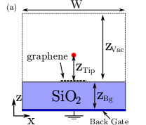
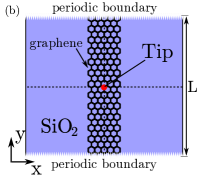
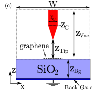
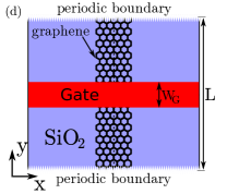
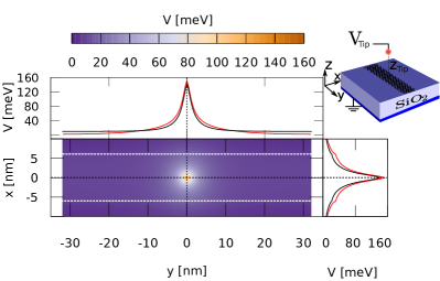
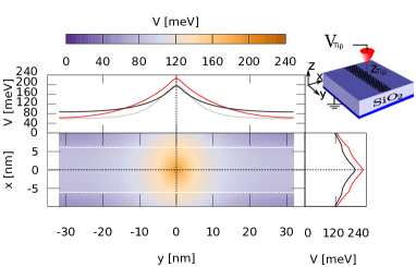
We consider (Fig. 1) a metallic and semiconducting armchair nanoribbon of width nm ( carbon atoms across the channel for the metallic ribbon and 97 atoms for the semiconducting one). On the bottom of the system we place the metallic back gate (Fig. 1(a,c)) which is covered by an insulating SiO2 layer nm thick. The graphene is deposited on top of the insulator (). For the top gate we use three models of the tip: (i) a point-like tip that occupies a single cell (Fig. 1(a,b)) of the finite difference mesh ( nm and nm), (ii) an extended cylindrical electrode ended with a cone tip 1(c)) and (iii) a rectangular gate perpendicular to the ribbon. The tip is placed above the graphene layer at the center of the ribbon, and the rectangular gate crosses the computation box symmetrically 1(d)).
a)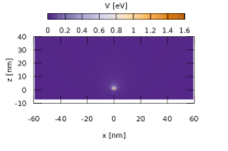 b)
b)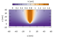
For graphene we apply the standard tight-binding Hamiltonian form for the electrons on the orbitals
| (1) |
where () is the creation (annihilation) operator of an electron at -th atom with spin and eV Castro Neto et al. (2009) for all nearest ions and elsewhere. The wave function for the -th eigenstate with spin is defined as a linear combination of atomic orbitals
| (2) |
with orbitals centered at the carbon atom positions. The interaction between electrons is taken into account by the Kohn-Sham potential of the form
| (3) |
where and are external potential, Hartree potential and ion potential, respectively. The exchange-correlation potential is taken in the Perdew-Zunger form Perdew and Zunger (1981). To proceed, we need to define electron-density and ion-density, first one has form
| (4) |
where is the Fermi-Dirac distribution function with orbital energy and Fermi energy in the temperature. The ion-density is defined as
| (5) |
We obtain the eigenstates of Hamiltonian (1) self-consistently using the Broyden Broyden (1965) mixing scheme. The calculations were performed for a finite temperature of K, to achieve convergence. For the Poisson equation, we use the finite difference method with the cubic cells. For that reason the charge density defined within the graphene ribbon is effectively spread over a finite thickness. The external potential is defined by the metallic bottom gate and the metallic point tip above the structure (see. Fig. 1). To calculate the entire potential of the system we solve the Poisson equation . The applied finite difference approach is explained in the Appendix.
For the studies of the transport near the Dirac point we take the total potential that is derived for the charge neutral system. For the charge neutrality point the potential is independent of the spin. For the potential on the bottom gate and on the tip we apply Dirichlet boundary conditions for fixed electrostatic potential. We set the bottom gate at (grounded) potential and vary the tip voltage. In order to simulate an infinite ribbon for evaluation of the potential profile in the direction we consider periodic boundary conditions with a box length equal to nm, with about 30 thousand carbon atoms inside the periodically repeated cell. We apply the Dirichlet boundary conditions for the bottom face of the box, where the backgate is applied. For the other faces we assume that the normal component of the field vanishes. On the side faces perpendicular to axis this condition is justified by the periodic boundary conditions. On the side faces perpendicular to the axis the condition is justified by a large distance from the tip, and – for the rectangular top gate – by the layer structure of the system. At the top face of the computational box the vanishing of the electric field for the floating point-like tip and for the rectangular gate is justified by the charge neutrality of the entire system. At a large distance from all the space charges the electric field, in particular its normal component vanishes. For the cone tip, the Neumann boundary condition at the top side is justified by the radial character of the potential induced by the cylindrical gate. The conditions for the top face are justified at a large distance from the graphene layer so the computation box needs to be large enough. To find an appropriate height of the computational box we calculate the potential energy profile on the graphene layer. The dependence is weak and we set nm as the value for which the convergence is reached. For the lateral size of the box we find that it is sufficient to set the side length nm, i.e., ten times wider than the ribbon (Fig. 1(b)). The potential at the graphene ribbon at the end of the box is set as a reference energy level for the transport calculations.
The size of the present model system is limited by the numerical complexity of the atomistic approach. Scaling approaches have been introduced for the tight binding models with the increase of the carbon-carbon distance that is compensated by the modification of the hopping parameters Liu et al. (2015b). In the present paper we keep the carbon-carbon distance unchanged and the considered system should be treated as a model with physical dimensions reduced by a factor of of the actual device. Accordingly, for the transport modeling we use the potential that is obtained for the tip at 1 nm above the graphene plane.
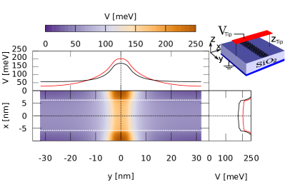
Fig. 2 shows the results for the floating point-like model of the tip for the metallic (black) and semiconducting (red) ribbon. The potential is screened more effectively by the electron gas in the metallic ribbon. We can see that the screening by the ribbon produces an anisotropy in the effective potential, with the maximum that is elongated perpendicular to the ribbon axis. This anisotropy and the dependence of the effectiveness of the screening on the type of the ribbon are also found for the cone-model of the tip plotted in Fig. 3. The cone model of the extended tip produces wider maximum than the point-like model. For illustration a cross-section of the potential for the tip models is given in Fig. 4. For the extended top-gate electrode [Fig. 5] the stronger screening by the metallic ribbon is evident.
II.2 Transport
The effective potential evaluated by the tip, including the screening by all the occupied single-electron energy levels below the Fermi level, is calculated in the absence of the external magnetic field. For the transport at the Fermi level we account for the external magnetic field modifying the hopping parameters of Eq. (1) with the Peierls phase , where is the vector potential. We use the gauge appropriate for the terminals using the approach proposed in Ref. Baranger and Stone, 1989. We take and apply a gauge transformation with , and a smooth step-like function that is 0 in the ribbon interior interior where the probes attached, and 1 for 24 nm . We introduce the spin Zeeman effect,
| (6) |
where is Bohr magneton, is the Pauli matrix, and .
For evaluation of the transmission probability, we use the wave function matching (WFM) technique Kolasiński et al. (2016). The transport calculations are performed for zero temperature. The leads feeding and draining current are considered semi-infinite. The partial transmission probability is evaluated as
| (7) |
where is the probability amplitude for the transmission from the mode with spin in the input lead to mode with spin in the output lead . The Hamiltonian (6) is spin-diagonal. We evaluate the conductance from lead to as , with . For a single spin . In our model the dephasing is defined by the coupling of the sample to the virtual probes . For fully coherent transport with the virtual probes detached () the two-terminal conductance is simply given by .
To take into account the dephasing, we use the Büttiker virtual probes Büttiker (1988) technique. The idea Büttiker (1988) is to introduce leads with zero net current fed to the system, i.e. an electron that enters the probe, gets to the reservoir and comes back to the system with a randomized phase. Technically, one solves the transport problem at the Fermi level for a model multiterminal device. In general, for a system with terminals, the conductance matrix is constructed, which translates the voltage to currents , with being the current flowing in the th terminal and the voltage measured at the th terminal. The matrix elements are calculated as
| (8) |
with
| (9) |
The currents in the leads are related by the Kirchhoff’s law, thus the matrix as given by Eqs. (8) and (9) is singular. After elimination of the current in the th terminal one obtains an invertible matrix. The resistance matrix is then evaluated by .
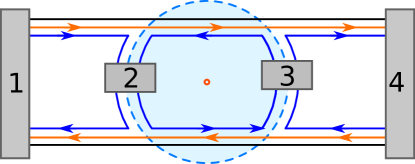
For the system with equilibration, we use two Büttiker probes, so the system has terminals in total as in Fig. 6. The net current flows from terminal 1 to terminal 4. Leads 2 and 3 are Büttiker voltage terminals with zero net current. The two-terminal conductance is given by
| (10) |
For the labeling of the terminals shown in Fig. 6, we set the potential of the lead 4 as a reference . The two-terminal conductance is then given by
| (11) |
For each of the terminals we solve the scattering problem with the WFM method to obtain , fill in the matrix, and compute the conductance (11). From now on we use the notation for the two-terminal conductance.
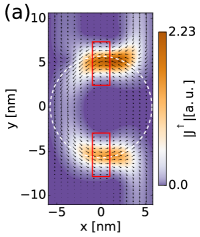
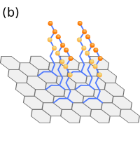
Let us describe the implementation of the Büttiker probes. For low Fermi energy the tip potential introduces an n-p junction to the ribbon. The p region within the n medium is either circular or it occupies the entire width of the ribbon. There are at most two bipolar junctions where the dephasing takes place. We connect voltage probes to the graphene plane near the ribbon axis at the position of the junction – Fig. 7. For the equilibration along the bipolar junctions in order to maximize the dephasing, the probe has to span across the junction (see red rectagles in Fig. 7(a)). The applied probes consist of a set of one-dimensional zigzag chains connected to the graphene as depicted in Fig. 7(b). The hopping between the graphene and the probe is , which is a parameter that allows us to switch on or off the dephasing probes from the system. Our probes consist of 99 zigzag chains connected to a common reservoir. The position is dynamically set to the position of the bipolar junction, i.e. the center of the probe is where for spin up (down) electrons. Note that the probes work effectively only when the system enters the quantum Hall regime and the current flows close to the edge and along the junctions and not in the entire width of the ribbon.
III Results
III.1 Fully coherent transport
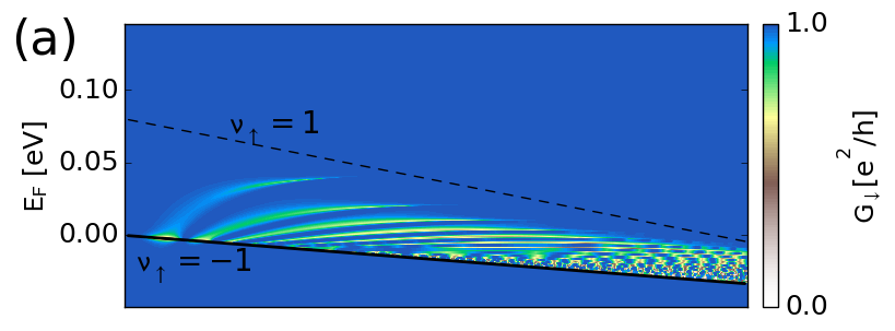
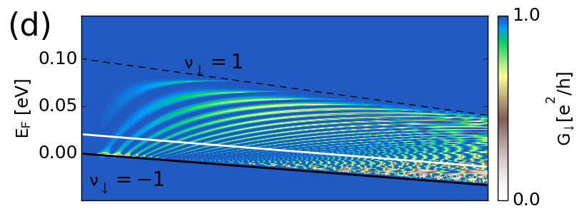
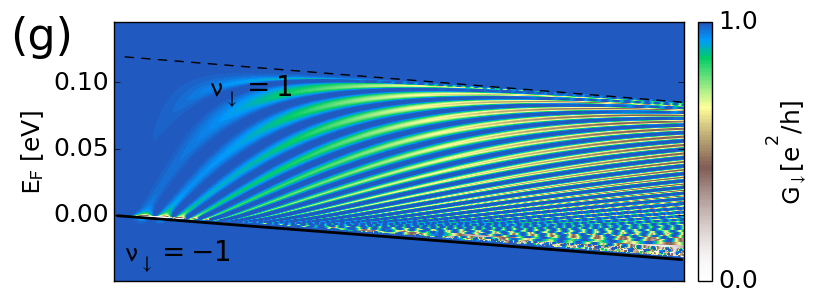
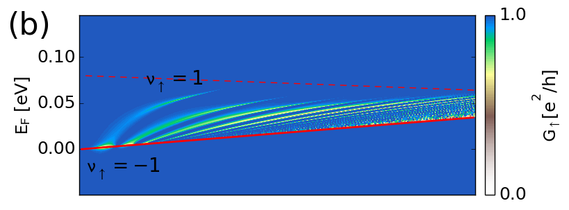
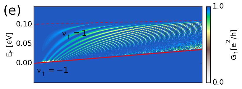
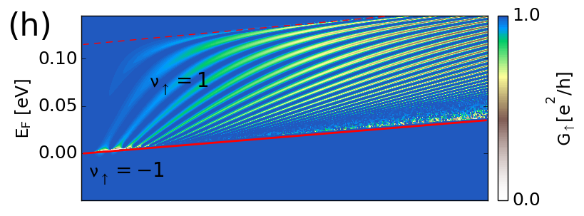
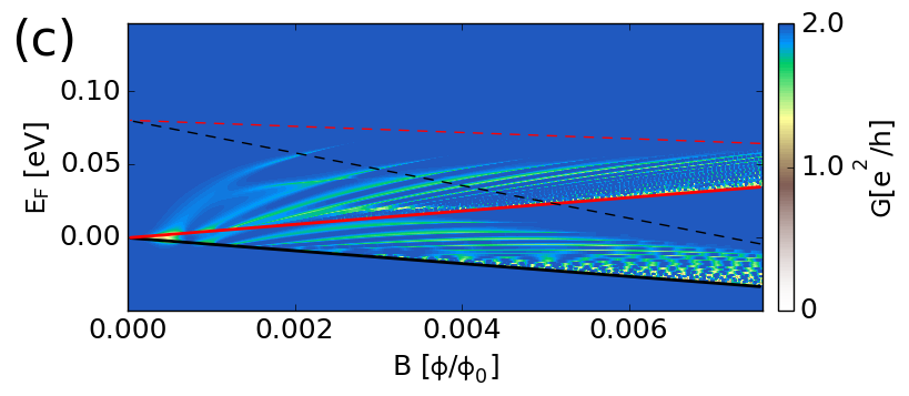
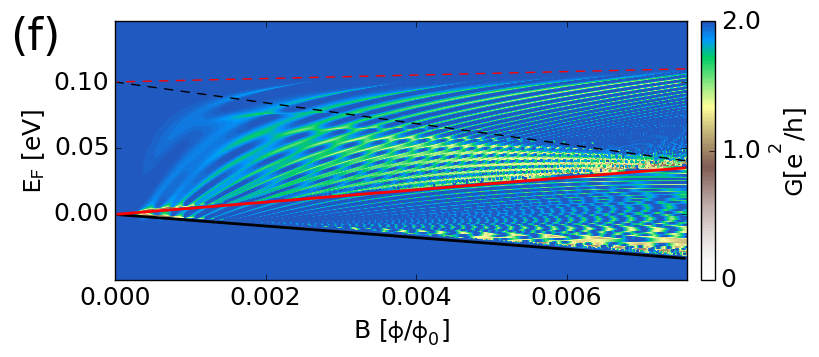
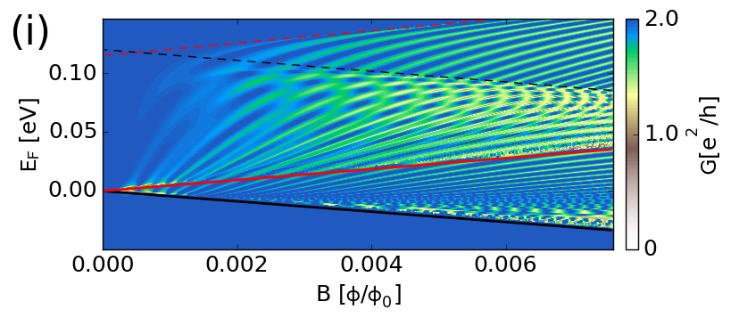
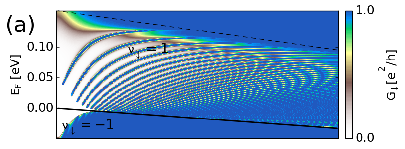
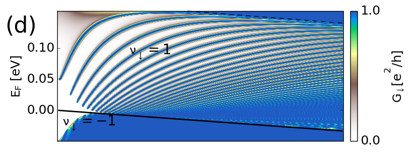
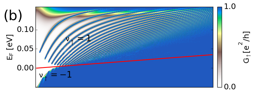
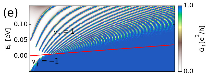
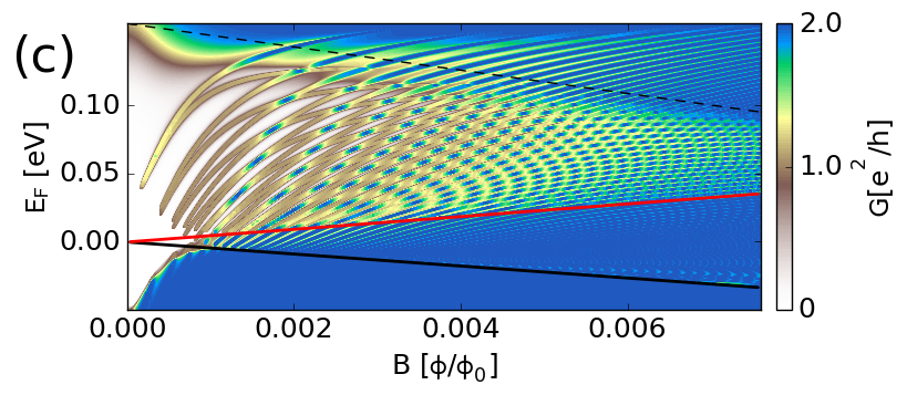
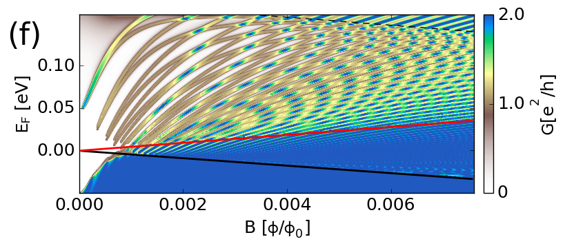
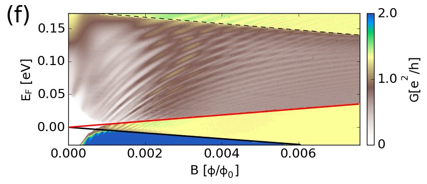
Let us first consider the fully coherent magnetotransport in the nanoribbons with tip-induced circular junction. Fig. 8 shows the spin down (a,d,g), spin up (b,e,h), and overall (c,f,i) conductance of a metallic nanoribbon, as a function of magnetic field through one graphene hexagon (, with nm, ) and Fermi energy. for T. The conductance is generally close to 2 with the exception of conductance oscillations involving the circular junction. The Dirac point for both directions of spin shifts in opposite energy, as indicated by red and black thick solid lines in Fig. 8.
Figures 8(a-c) show the results for a potential profile calculated for a point-like tip. The island within the area in Fig. 8 is formed above the solid line – indicating the Dirac point. Above the threshold shown by dashed red (black) line for spin up (down) the oscillations vanish as the radius of the junction gets so small that the edge states no longer couple to the states around the junction.
Figures 8(d-f) present the conductance for tip modeled as a cone. For such a potential profile the n-p junction is more extended, and therefore it can reach the edges of the ribbon for higher carrier energies than in the case of point-like tip. Thus the oscillations occur in a broader range of energies than for the results in Fig. 8(a-c). Still, the higher the magnetic field, the narrower the extent of the wave functions flowing in the ribbon, thus the coupling to the junction gets smaller.
In the Figures 8(g-i) the results for a flat electrode are shown. In this case the dashed line shows where the sum of Fermi and Zeeman energy exceed the maximal potential energy of the induced n-p junction.
The Aharonov-Bohm periodicity of conductance is related to the area of the effective island by the formula . The area and the period are similar for the structures considered in Fig. 8.
Figure 9 presents the spin down (a,d), spin up (b,e), and overall (c,f) conductance of a semiconducting nanoribbon, for the potential due to a cone-shaped tip and for the flat gate potential. The difference with respect to the metallic nanoribbon is that the amplitude of the oscillations is much higher, as previously reported in Ref. Mreńca-Kolasińska et al. (2016).
III.2 Equilibration
The conductance of a bipolar junction with equilibrated currents and filling factors in a spin-degenerate system is given by Özyilmaz et al. (2007):
| (12) |
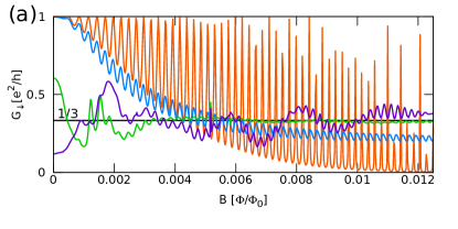
Here the filling factor is summed over spins. For instance in a spin degenerate system with filling factors in the junction , the conductance with complete equilibration is . The channel mixing is only between channels of the same spin (Amet et al., 2014b; Wei et al., 2017). For each of the spins the conductance is , giving , and the overall conductance is the sum .
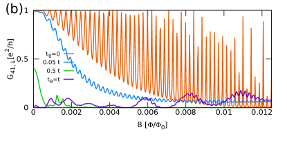
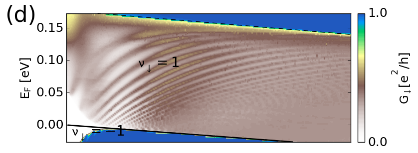
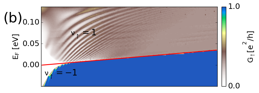
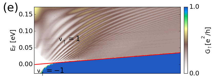
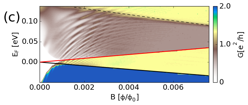
Fig. 10(a) shows the cross-section of Fig. 8(d) along the white inclined line for varied parameter . Clearly the oscillations for have the highest amplitude, and for growing their amplitude is more and more suppressed. For , at high magnetic field limit, the conductance saturates at . In Fig. 10(a) the conductance matrix element derived directly from the quantum scattering problem is presented for comparison. For the visibility of conductance oscillation is distinctly larger in the two-terminal conductance than in the matrix element, and the two-terminal conductance is non-zero for at high magnetic field, although the matrix element vanishes. The vanishing of coincides with the saturation of the two-terminal conductance at , since all the electrons flow into the virtual leads and do not reach the output lead.
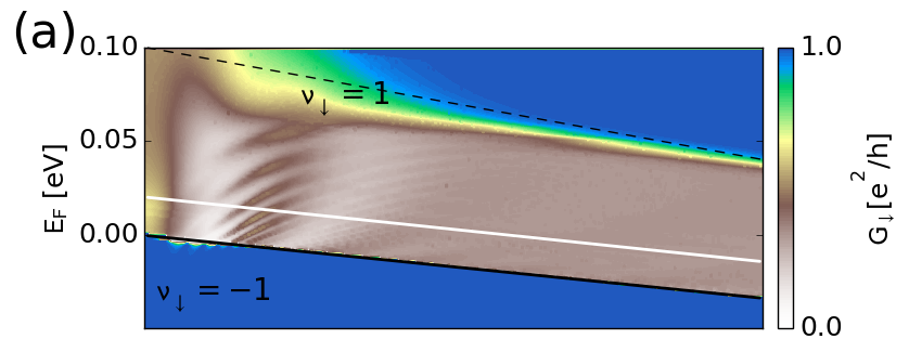
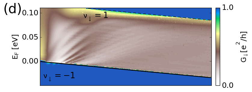
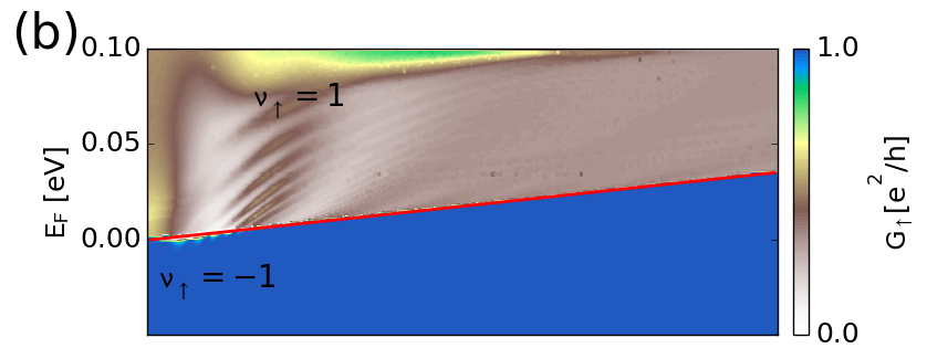
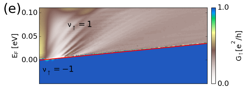
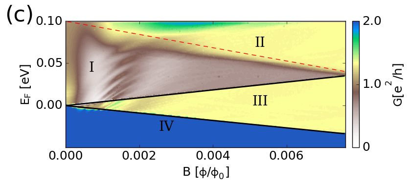
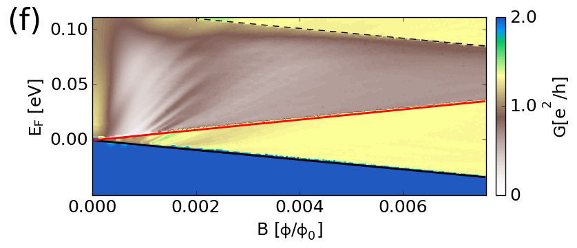
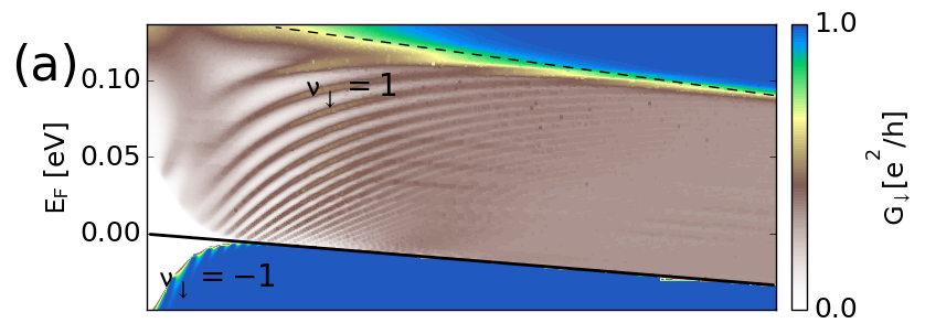
Figure 11 (Figure 12) shows the conductance as a function of magnetic field and Fermi energy for the metallic (semiconducting) ribbon in presence of the equilibration. In both cases the oscillations that were present for the fully coherent transport in Fig. 8 and Fig. 9 are suppressed at high magnetic field. In the limit of strong dephasing the results for the semiconducting and metallic ribbon becomes nearly identical.
III.3 Discussion
The results for equilibrated currents shown above involved electron and hole channels from the zeroth Landau level along the bipolar junction. Whenever there is a bipolar junction in the considered nanoribbon, in the region under the tip and beyond there are only the channels from the lowest Landau level for magnetic field sufficiently high for the Hall effect to occur. For low Fermi energy when the junction diameter is bigger than the width of the ribbon, a nearly rectangular junction is induced. For such system with filling factors in the regions, respectively, the conductance with complete equilibration is predicted to be Özyilmaz et al. (2007). In pure graphene the spin-orbit coupling is negligible thus the mixing occurs only between same-spin channels (Amet et al., 2014b; Wei et al., 2017).
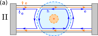
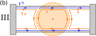
In our study, we take into account the Zeeman splitting in the transport. In high magnetic field, the system can be tuned into configurations of filling factors with opposite spins, e.g. shown in Fig. 13, and to conditions where the Fermi level is aligned with the conduction band of one spin direction and with the valence band for the other. The coexistence of the electron and hole states close to neutrality point has been presented for graphene deposited on SiO2 substrate Wiedmann et al. (2011); Abanin et al. (2007). However, samples on hexagonal boron nitride can be strongly insulating close to the neutrality point which was attributed by the valley symmetry breaking by the substrate Hunt et al. (2013); Amet et al. (2013) with incommensurate lattice constant.
For the energy below the thick black line in Fig. 11, in the region labeled by IV for both spins there is a single hole channel in the entire ribbon, and no bipolar junction occurs. The channels are transfered without backscattering and the conductance is . In the region labeled by I for both spin orientation there is a single electron channel outside the tip potential and a single-hole channel under the tip. For a complete equilibration each of the spins should contribute to the overall conductance. For in region I of Fig. 11 the conductance still oscillates near . In the region III, for spin down carriers an junction forms, and for spin up only hole-conductance occurs as shown schematically in Fig. 13(b). Thus with a complete equilibration, the spin down current contributes and spin up , and the summed conductance is . On the other hand, in the region labeled by II for spin up there is a broad junction. For spin down the Fermi energy is so high that either there is no junction or it has a very small radius so that the junction states are decoupled from the edge states, resulting in a lack of backscattering. Thus , , and again . This situation is shown schematically in Fig. 13(a). In the numerical calculations we obtain for regions II and III conductance close to with only very small oscillations that vanish slowly in the high magnetc field limit.
IV Summary and Conclusions
We studied an electron interferometer induced by potential of a floating gate within a graphene nanoribbon in the quantum Hall conditions. A numerical description of the transport conditions was given with the atomistic tight-binding Hamiltionian, tip potential derived from the electrostatics of the device and Büttiker virtual probes inducing dephasing effects at the junctions. The transport phenomena occurring in the interferometer involve the coherent Aharonov-Bohm oscillations and incoherent equilibration process resulting in appearance of fractional conductance plateaus. An interplay of the conductance oscillations and quantum Hall effects was explained.
We pointed out that the metallic ribbon is more effective in the screening of the top gate potential, that the visibility of the coherent conductance oscillation is much larger for the semiconducting ribbon and that in the strong dephasing limit of a complete equilibration the same results are obtained for the metallic and semiconducting ribbons with the fractional conductance plateaus replacing the current oscillations.
Acknowledgments
This work was supported by the National Science Centre (NCN) according to decision DEC-2015/17/B/ST3/01161 and by AGH UST budget with the subsidy of the Ministry of Science and Higher Education, Poland with Grant No. 15.11.220.718/6 for young researchers and Statutory Task No. 11.11.220.01/2. The calculations were performed on PL-Grid Infrastructure.
V Appendix: finite difference approach for the Poisson equation
To obtain the entire potential in the structure, we solve the Poisson equation
| (13) |
where is the electron density originating from the spatial distribution of the electrons in graphene flake and it lies exactly at the interface between two media (see Fig. 1(a)) i.e. for . The charge density is defined on the hexagonal graphene lattice. We effectively spread this quantity over the entire ribbon with finite thickness of . The - dependent dielectric constant is equal for (the Silicon Dioxide substrate) and for (vacuum). In the regions where the equation (13) simplifies to
| (14) |
which is charge-free Laplace equation.
We solve this equation numerically with finite difference method. We work on 3D cartesian grid with grid spacing equals to nm and nm and the total number of grid points .
For the charge-free equation (15) we simply use the seven-point stencil (see Fig. 14 (a)) that produces the set of equation in the form
| (15) |
with , where tuple represents the point on the discretized 3D lattice.
In the region where , one needs to take into the consideration a steep change of and the presence of the right hand side of the equation (electron density distribution). As changes abruptly at the interface between media, we discretize it on the lattice shifted by half a step in the direction (see Fig. 14), while potential discretization grid stays the same. With these settings, we arrive at the system of equations of the form
| (16) |
with defined as average between point i.e. .
To solve equations (15) and (16) we need to define the boundary conditions. We consider Dirichlet and Neumann boundary conditions in this work. The first one accounts for the metallic gates: the bottom gate and the tip. This type of boundary is incorporated into the grid equations by setting , where tuple stands for the point on the boundary, and is the gate potential. The Neumann boundary is responsible for vanishing of an electric field in the direction normal to the boundary, . To use this equation for a top wall, we discretize the condition in the direction obtaining
| (17) |
and plug this into the equations (15). For the side walls we use this condition in the same manner with a different direction of the normal vector . To solve this set of equations we use the iterative successive over-relaxation method (SOR). For convergence, we check the norm of the grid points and we stop if difference between iterations is less than V.
After convergence is reached we have solution defined on the Cartesian grid. To obtain the value of the potential for the graphene lattice point (see Fig. 14 (b)) we interpolate its value as , where the coefficients are the solution of the set of equations given by
a)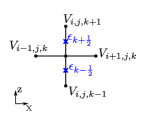 b)
b)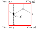
References
- Castro Neto et al. (2009) A. H. Castro Neto, F. Guinea, N. M. R. Peres, K. S. Novoselov, and A. K. Geim, Rev. Mod. Phys. 81, 109 (2009).
- Bolotin et al. (2008) K. Bolotin, K. Sikes, Z. Jiang, M. Klima, G. Fudenberg, J. Hone, P. Kim, and H. Stormer, Solid State Commun. 146, 351 (2008).
- Banszerus et al. (2016) L. Banszerus, M. Schmitz, S. Engels, M. Goldsche, K. Watanabe, T. Taniguchi, B. Beschoten, and C. Stampfer, Nano Lett. 16, 1387 (2016).
- Miao et al. (2007) F. Miao, S. Wijeratne, Y. Zhang, U. C. Coskun, W. Bao, and C. N. Lau, Science 317, 1530 (2007).
- Chen et al. (2016) S. Chen, Z. Han, M. M. Elahi, K. M. M. Habib, L. Wang, B. Wen, Y. Gao, T. Taniguchi, K. Watanabe, J. Hone, A. W. Ghosh, and C. R. Dean, Science 353, 1522 (2016).
- Rickhaus et al. (2013) P. Rickhaus, R. Maurand, M.-H. Liu, M. Weiss, K. Richter, and C. Schönenberger, Nat. Commun. 4, 2342 (2013).
- Taychatanapat et al. (2015) T. Taychatanapat, J. Y. Tan, Y. Yeo, K. Watanabe, T. Taniguchi, and B. Özyilmaz, Nat. Commun. 6, 6093 (2015).
- Lee et al. (2015) G.-H. Lee, G.-H. Park, and H.-J. Lee, Nat. Phys. 11, 925 (2015).
- Liu et al. (2017) M.-H. Liu, C. Gorini, and K. Richter, Phys. Rev. Lett. 118, 066801 (2017).
- Shytov et al. (2008) A. V. Shytov, M. S. Rudner, and L. S. Levitov, Phys. Rev. Lett. 101, 156804 (2008).
- Young and Kim (2009) A. F. Young and P. Kim, Nat. Phys. 5, 222 (2009).
- Grushina et al. (2013) A. L. Grushina, D.-K. Ki, and A. F. Morpurgo, Appl. Phys. Lett. 102, 223102 (2013).
- Russo et al. (2008) S. Russo, J. B. Oostinga, D. Wehenkel, H. B. Heersche, S. S. Sobhani, L. M. K. Vandersypen, and A. F. Morpurgo, Phys. Rev. B 77, 085413 (2008).
- Huefner et al. (2010) M. Huefner, F. Molitor, A. Jacobsen, A. Pioda, C. Stampfer, K. Ensslin, and T. Ihn, New J. Phys. 12, 043054 (2010).
- Smirnov et al. (2012) D. Smirnov, H. Schmidt, and R. J. Haug, Appl. Phys. Lett. 100, 203114 (2012).
- Rahman et al. (2013) A. Rahman, J. W. Guikema, S. H. Lee, and N. Marković, Phys. Rev. B 87, 081401(R) (2013).
- Smirnov et al. (2014) D. Smirnov, J. C. Rode, and R. J. Haug, Appl. Phys. Lett. 105 (2014).
- Cabosart et al. (2014) D. Cabosart, S. Faniel, F. Martins, B. Brun, A. Felten, V. Bayot, and B. Hackens, Phys. Rev. B 90, 205433 (2014).
- Barbier et al. (2012) M. Barbier, G. Papp, and F. M. Peeters, Applied Physics Letters 100, 163121 (2012).
- Davies et al. (2012) N. Davies, A. A. Patel, A. Cortijo, V. Cheianov, F. Guinea, and V. I. Fal’ko, Phys. Rev. B 85, 155433 (2012).
- Williams and Marcus (2011) J. R. Williams and C. M. Marcus, Phys. Rev. Lett. 107, 046602 (2011).
- Carmier et al. (2011) P. Carmier, C. Lewenkopf, and D. Ullmo, Phys. Rev. B 84, 195428 (2011).
- Chen et al. (2012) J.-C. Chen, X. C. Xie, and Q.-F. Sun, Phys. Rev. B 86, 035429 (2012).
- Cresti et al. (2008) A. Cresti, G. Grosso, and G. P. Parravicini, Phys. Rev. B 77, 115408 (2008).
- Milovanović et al. (2014) S. P. Milovanović, M. R. Masir, and F. M. Peeters, J. Appl. Phys. 115, 043719 (2014).
- Milovanović et al. (2014) S. P. Milovanović, M. Ramezani Masir, and F. M. Peeters, Appl. Phys. Lett. 105, 123507 (2014).
- Rickhaus et al. (2015) P. Rickhaus, P. Makk, M.-H. Liu, E. Tóvári, Endre, M. Weiss, R. Maurand, K. Richter, and C. Schönenberger, Nat. Commun. 6, 6470 (2015).
- Liu et al. (2015a) Y. Liu, R. P. Tiwari, M. Brada, C. Bruder, F. V. Kusmartsev, and E. J. Mele, Phys. Rev. B 92, 235438 (2015a).
- Zarenia et al. (2013) M. Zarenia, J. M. Pereira, F. M. Peeters, and G. A. Farias, Phys. Rev. B 87, 035426 (2013).
- Oroszlány et al. (2008) L. Oroszlány, P. Rakyta, A. Kormányos, C. J. Lambert, and J. Cserti, Phys. Rev. B 77, 081403 (2008).
- Kolasiński et al. (2017) K. Kolasiński, A. Mreńca-Kolasińska, and B. Szafran, Phys. Rev. B 95, 045304 (2017).
- Müller (1992) J. E. Müller, Phys. Rev. Lett. 68, 385 (1992).
- Williams et al. (2011) J. R. Williams, T. Low, M. S. Lundstrom, and C. M. Marcus, Nat. Nanotech. 6, 222 (2011).
- Tovari et al. (2016) E. Tovari, P. Makk, M.-H. Liu, P. Rickhaus, Z. Kovacs-Krausz, K. Richter, C. Schonenberger, and S. Csonka, Nanoscale 8, 19910 (2016).
- Bours et al. (2017) L. Bours, S. Guiducci, A. Mreńca-Kolasińska, B. Szafran, J. C. Maan, and S. Heun, Phys. Rev. B 96, 195423 (2017).
- Mreńca-Kolasińska et al. (2016) A. Mreńca-Kolasińska, S. Heun, and B. Szafran, Phys. Rev. B 93, 125411 (2016).
- Recher et al. (2007) P. Recher, B. Trauzettel, A. Rycerz, Y. M. Blanter, C. W. J. Beenakker, and A. F. Morpurgo, Phys. Rev. B 76, 235404 (2007).
- Hewageegana and Apalkov (2008) P. Hewageegana and V. Apalkov, Phys. Rev. B 77, 245426 (2008).
- Abergel et al. (2008) D. S. L. Abergel, V. M. Apalkov, and T. Chakraborty, Phys. Rev. B 78, 193405 (2008).
- Jackiw et al. (2009) R. Jackiw, A. I. Milstein, S.-Y. Pi, and I. S. Terekhov, Phys. Rev. B 80, 033413 (2009).
- Schelter et al. (2010) J. Schelter, D. Bohr, and B. Trauzettel, Phys. Rev. B 81, 195441 (2010).
- Wurm et al. (2010) J. Wurm, M. Wimmer, H. U. Baranger, and K. Richter, Semicond. Sci. Technol. 25, 034003 (2010).
- Wu et al. (2010) Z. Wu, Z. Z. Zhang, K. Chang, and F. M. Peeters, Nanotechnol. 21, 185201 (2010).
- Downing et al. (2011) C. A. Downing, D. A. Stone, and M. E. Portnoi, Phys. Rev. B 84, 155437 (2011).
- Faria et al. (2013) D. Faria, A. Latgé, S. E. Ulloa, and N. Sandler, Phys. Rev. B 87, 241403 (2013).
- da Costa et al. (2014) D. R. da Costa, A. Chaves, M. Zarenia, J. M. Pereira, G. A. Farias, and F. M. Peeters, Phys. Rev. B 89, 075418 (2014).
- Rakyta et al. (2014) P. Rakyta, E. Tóvári, M. Csontos, S. Csonka, A. Csordás, and J. Cserti, Phys. Rev. B 90, 125428 (2014).
- Abanin and Levitov (2007) D. A. Abanin and L. S. Levitov, Science 317, 641 (2007).
- Williams et al. (2007) J. R. Williams, L. DiCarlo, and C. M. Marcus, Science 317, 638 (2007).
- Özyilmaz et al. (2007) B. Özyilmaz, P. Jarillo-Herrero, D. Efetov, D. A. Abanin, L. S. Levitov, and P. Kim, Phys. Rev. Lett. 99, 166804 (2007).
- LaGasse and Lee (2016) S. W. LaGasse and J. U. Lee, Phys. Rev. B 94, 165312 (2016).
- Alphenaar et al. (1990) B. W. Alphenaar, P. L. McEuen, R. G. Wheeler, and R. N. Sacks, Phys. Rev. Lett. 64, 677 (1990).
- Amet et al. (2014a) F. Amet, J. Willams, K. Watanabe, T. Taniguchi, and D. Goldhaber-Gordon, Phys. Rev. Lett. 112, 196601 (2014a).
- Geim and Grigorieva (2013) A. Geim and I. Grigorieva, Nature 499, 419 (2013).
- Wei et al. (2017) D. S. Wei, T. van der Sar, J. D. Sanchez-Yamagishi, K. Watanabe, T. Taniguchi, P. Jarillo-Herrero, B. I. Halperin, and A. Yacoby, Sci. Adv. 3, e1700600 (2017).
- Makk et al. (2018) P. Makk, C. Handschin, E. Tovari, K. Watanabe, T. T., K. Richter, M.-H. Liur, and C. Schoenenberger, Phys. Rev. B 98, 035413 (2018).
- Morikawa et al. (2015) S. Morikawa, S. Masubuchu, R. Moriya, K. Watanabe, T. T., and T. Machida, Appl. Phys. Lett. 106, 183101 (2015).
- Büttiker (1988) M. Büttiker, Phys. Rev. B 38, 9375 (1988).
- Myoung and Park (2017) N. Myoung and H. C. Park, Phys. Rev. B 96, 235435 (2017).
- Long et al. (2008) W. Long, Q.-f. Sun, and J. Wang, Phys. Rev. Lett. 101, 166806 (2008).
- Chen et al. (2011) J.-C. Chen, H. Zhang, S.-Q. Shen, and Q.-F. Sun, J. Phys.: Condens. Matter 23, 495301 (2011).
- Perdew and Zunger (1981) J. P. Perdew and A. Zunger, Phys. Rev. B 23, 5048 (1981).
- Broyden (1965) C. G. Broyden, Math. Comput. 19, 577 (1965).
- Liu et al. (2015b) M.-H. Liu, P. Rickhaus, P. Makk, E. Tóvári, R. Maurand, F. Tkatschenko, M. Weiss, C. Schönenberger, and K. Richter, Phys. Rev. Lett. 114, 036601 (2015b).
- Baranger and Stone (1989) H. U. Baranger and A. D. Stone, Phys. Rev. B 40, 8169 (1989).
- Kolasiński et al. (2016) K. Kolasiński, B. Szafran, B. Brun, and H. Sellier, Phys. Rev. B 94, 075301 (2016).
- Amet et al. (2014b) F. Amet, J. R. Williams, K. Watanabe, T. Taniguchi, and D. Goldhaber-Gordon, Phys. Rev. Lett. 112, 196601 (2014b).
- Wiedmann et al. (2011) S. Wiedmann, H. J. van Elferen, E. V. Kurganova, M. I. Katsnelson, A. J. M. Giesbers, A. Veligura, B. J. van Wees, R. V. Gorbachev, K. S. Novoselov, J. C. Maan, and U. Zeitler, Phys. Rev. B 84, 115314 (2011).
- Abanin et al. (2007) D. A. Abanin, K. S. Novoselov, U. Zeitler, P. A. Lee, A. K. Geim, and L. S. Levitov, Phys. Rev. Lett. 98, 196806 (2007).
- Hunt et al. (2013) B. Hunt, J. D. Sanchez-Yamagishi, A. F. Young, M. Yankowitz, B. J. LeRoy, K. Watanabe, T. Taniguchi, P. Moon, M. Koshino, P. Jarillo-Herrero, and R. C. Ashoori, Science 340, 1427 (2013).
- Amet et al. (2013) F. Amet, J. R. Williams, K. Watanabe, T. Taniguchi, and D. Goldhaber-Gordon, Phys. Rev. Lett. 110, 216601 (2013).