Field-effect-driven half-metallic multilayer graphene
Abstract
Rhombohedral stacked multilayer graphene displays the occurrence of a magnetic surface state at low temperatures. Recent angular resolved photoemission experiments demonstrate the robustness of the magnetic state in long sequences of ABC graphene. Here, by using first-principles calculations, we show that field-effect doping of these graphene multilayers induces a perfect half-metallic behaviour with 100% of spin current polarization already at dopings attainable in conventional field effect transistors with solid state dielectrics. Our work demonstrates the realisability of a new kind of spintronic devices where the transition between the low resistance and the high resistance state is driven only by electric fields.
The realization of modern spintronic devices such as lateral spin-valvesFukuma et al. (2011), spin-hall effect devices and spin transfer torque memoriesLiu et al. (2012); Lesne et al. (2016) requires injection of spin-polarized currents. Materials of choice for such devices are half-metals, namely compounds conducting in one spin channel and insulating in the otherde Groot et al. (1983); Katsnelson et al. (2008), like Heussler alloys and some transition metal oxidesKatsnelson et al. (2008). In many of these systems, however, the surface conduction limits the amount of polarized current. Materials with a perfect half-metallic behavior not only in the bulk but also at the surface are needed. Half-metallicity embedded in surface or edge states of an easily processable material like carbon would be an ideal solution to the problem. However, carbon is not magnetic in its bulk forms.
Most of the search for half-metallic materials focused initially on ferromagnets and ferrimagnets, as in conventional antiferromagnets the cancellation of magnetic moments is due to symmetry operations connecting sites of opposite spin. The same symmetry relations cause the bands for the two spin directions to be degenerate, forbidding a polarization of conduction electrons.van Leuken and de Groot (1995) As a consequence, breaking the symmetry equivalence between sites is necessary to obtain a half-metallic material from an antiferromagnet. This can be done by substituting one of the magnetic centers in such a way that the net magnetic moment remains zero. The resulting material is known as a spin compensated antiferromagnet and can be conceptualized as a special case of ferrimagnet with zero magnetic moment. Just as the ferrimagnetic case, the bands are not degenerate and half-metallicity can occur. van Leuken and de Groot (1995); Akai and Ogura (2006)
An alternative route is to introduce a symmetry-breaking perturbation in the antiferromagnetic material. This can lift the degeneracy while changing very little the net magnetization, with spins preserving an essentially antiferromagnetic configuration. Introducing such perturbation is possible if the spins of opposite orientation are spatially separated in the material. In the special case where they are localised at edges or surfaces, applying a static electric field is sufficient to break the symmetry and possibly induce a half-metallic state.
In a seminal paper, Son et al.Son et al. (2006) showed that graphene nanoribbons have magnetic edge states and would turn into half-metallic ferromagnets under the application of an electric field. This finding has generated substantial interest,Guo et al. (2008); Kan et al. (2007); Yang-Yang et al. (2015); Wu et al. (2009); Kim and Kim (2008); Jung and MacDonald (2010) and received some preliminary experimental confirmation.Joly et al. (2010) However, no such device has in practice been realized, since it would require application of very strong fields of the order of 0.1 V/Å along the plane parallel to the nanoribbonSon et al. (2006).
Previous theoretical work based on the Hubbard model applied to bilayer grapheneYuan et al. (2013) suggested that an electric field combined wih doping could induce an half-metallic state. However, as the gap in bilayer graphene is only meV and the energy difference between up and down spin states is of the same order, the magnetic state would be destroyed already at 10-20 K. For the same reason a low degree of spin polarization can be expected in this system at finite temperatures.
A way to overcome these difficulties is to consider rhombohedral stacked multilayer graphene (RMG). These systems present magnetic surface state and a sizeable gap, as large as 40 meV in RMG trilayers, more than one order of magnitude larger than in the case of bilayer graphene.Pamuk et al. (2017); Lee et al. (2014); Throckmorton and Vafek (2012); Xu et al. (2012); Henck et al. (2017) Rhombohedral or ABC stacking is a metastable phase of graphite which coexists with the more common AB (or Bernal) stacking.Lipson and Stokes (1942) Natural graphite samples contain a substantial percentage of ABC graphiteLipson and Stokes (1942); Lui et al. (2011). RMG can be obtained by exfoliationLee et al. (2014); Henni et al. (2016) and identified through Raman spectroscopyTorche et al. (2017) or magneto-optic experimentsHenni et al. (2016), as well as grown directly on a SiC substratePierucci et al. (2015).
In this paper, by using first principles electronic structure calculationsabi , we analyze the magnetic surface state of long series of RMG and show that it becomes a half metal by doping the sample with the application of a realistic electric field in a field-effect transistor (FET) configuration. We calculate amount of spin polarized conduction, finding that doping charge densities as low as are sufficient to induce the half metallic behaviour and to achieve a completely polarized spin current. At liquid nitrogen temperature the spin polarization is still 90%.
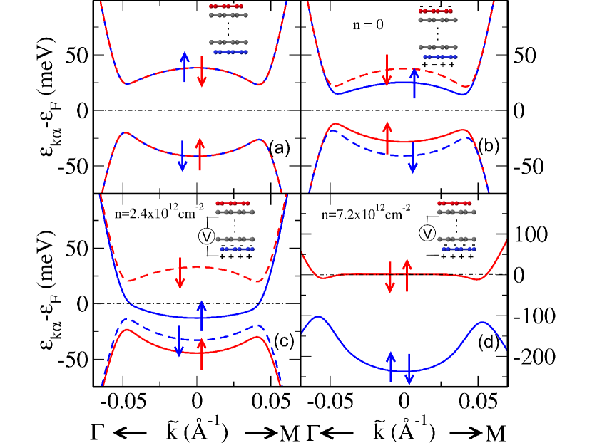
By neglecting spin polarization undoped RMG is a metal with an extremely flat surface band at the Fermi level centered at the special point K of the Brillouin zonePamuk et al. (2017). The surface state is formed by the orbitals of only one of the two atoms on each surface layer. This state is, however, unstable in the spin channel, leading to a magnetic state and a gap opening at low temperature, as shown in in Fig. 1 (a). Different magnetic instabilities are in principle possible,Lee et al. (2014) however the ground state was found to be globally antiferromagnetic, with the atoms in the top graphene layer having opposite spin polarizations with respect to those in the bottom one, and ferrimagnetic within each layer.Pamuk et al. (2017) As a result the energy bands are twofold degenerate in the spin channel. The spin density decays rapidly inside the multilayer. The fraction of electrons contained in the surface state increases with increasing thickness, as does the band gap which however saturates at 56 meV for 6 layers.Pamuk et al. (2017) In thicker multilayers the gap decreases slowly, approaching the band structure of bulk ABC graphite which shows Dirac points along the -K and K-M lines.
Transport measurements Lee et al. (2014) on suspended ABC trilayers confirm the opening of a 42 meV gap, in agreement with theoretical calculations. The Néel critical temperature () as measured in transport was found to be K. More recently, ARPES experiments on thicker samplesHenck et al. (2017) (15 layers) demonstrated clearly the opening of a band gap, interpreted as due to magnetism, and a much higher , larger than liquid nitrogen temperature. Thus, both theoretical calculations and experimental data point to a true antiferromagnet with antiferromagnetic in-plane and out-of-plane couplings. For potential applications it is much more promising to consider thick multilayers of RMG (6 to 20 layers) as the gap is larger, magnetism more robust and the interaction with the substrate weaker.
The inversion symmetry in RMG can be broken by applying an external electric field. In this case, the top and bottom graphene layers are not anymore equivalent and the spin degeneracy is broken, as shown in Fig. 1 (b). The system is still insulating, however, the bottom of the conduction band is now formed by the up spin states of the layer at the higher electrostatic potential and the top of the valence band by the down spin states of the opposite layer. Thus, applying moderate electric fields breaks the spin degeneracy, reduces the gap but does not the remove the insulating state and does not generate a half-metallic state. Much larger electric fields are necessary to close the gap and form a metallic state in the spirit of Ref. Son et al., 2006.
An alternative way to reach a half-metallic state is to doping RMG in a FET setup. In this case, a gate dielectric is used and the RMG sample is one of the two plates of the capacitor, as done in Refs. Schwierz, 2010; Radisavljevic et al., 2011; Ye et al., 2012. This is shown schematically in the inset of Figs. 1 (c) and (d). The inversion symmetry is broken by the electric field and a doping charge is introduced on the surface in contact with the dielectric. This configuration can be simulated from first principles by neglecting the gate dielectric and placing the system in front of a charged layer, while doping it with the same amount of electrons obtaining overall charge neutrality.fet
At small doping, the extra charge is confined to the layer closest to the gate (i.e. the layer of point charges in the insets of Fig. 1 (c) and (d)) and decays inside the multilayer very quickly. The charge fills the unoccupied surface band associated with the layer closest to the point charges. Because unoccupied surface states of oppositely oriented spins are localized at opposite surfaces, all the doping charge will be spin polarized until the state located on the side of the gate is completely filled, generating a half-metallic state as shown in Fig. 1 (c).
For 12-layers, the half-metallicity persists up to a doping charge density of about , at which value the Fermi level crosses the spin down bands and magnetism is lost, as shown in Fig. 2 (a) and (b). At larger doping the bands become again doubly degenerate in the spin channel. The completely occupied electronic band is then formed by the states of one of the two atoms in the surface with higher electrostatic potential, while the partially occupied one is formed by the states of one of the atoms in the opposite layer. The half-metallic nature is lost and the system becomes a metallic paramagnet, as shown in Fig. 1 (d).
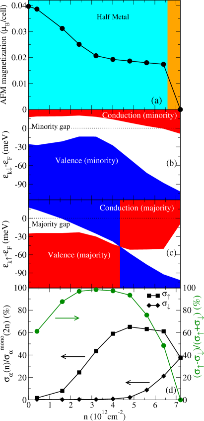
The value of critical doping at which half-metallicity disappears depends on the number of electrons contained in the surface band, and as a consequence, increases with multilayer thickness.Pamuk et al. (2017) Thicker samples result in flatter surface bands, that can in turn contain more electrons. Half metallicity is not only stronger in thicker samples but it also occurs in a larger range of doping and voltage.
Half-metallicity is not, by itself, enough to obtain a completely spin polarized current at finite temperature, as electrons could occupy minority spin states above the Fermi level when thermally excited. However, at a low doping level the minority spin states closest to the Fermi level are at a distance of meV K, as shown in Fig. 2 (b). Nearly perfect spin filtering should then occur at low temperatures. Conversely, at liquid nitrogen or higher temperatures, a finite number of minority spin electrons (and a smaller number of holes) contributes to the conduction. Within the constant relaxation-time approximation, where is the Fermi momentum, the in-plane conductivity for the spin channel in the direction of a transversal in-plane electric field in the direction can be expressed as:
| (1) |
where is the number of k-points, is the surface of the 2D unit cell, is the Fermi function, is the group velocity and is the relaxation time, approximated here by a constant. This conductivity can be compared to that of monolayer graphene, namely with and eVÅ , i. e. the PBE0 value, and . Assuming that n-doped monolayer graphene has similar scattering time to RMG at the same (i.e. at twice larger doping in monolayer graphene than in RMG), the ratio of becomes independent of . This quantity is shown in the bottom panel of Fig. 2. Despite the flattening of the bottom of the bands, in the doped case, the Fermi velocity is comparable to that of monolayer graphene. This results in a sizeable conductivity in the majority spin channel. On the contrary, in the minority spin channel the velocity of the thermally activated electrons remain very small. The polarization of the conductivity approaches 100% around . For thinner multilayers, the unoccupied minority spin band is closer to the Fermi level, but the occupied one is further away. While the half-metallic state is less robust, holes do not contribute to the minority spin conductance. The results for 6 layers RMG are provided in the Supplemental informationsup . The qualitative behavior of the current polarization is similar to the 12 layer case but in a narrower range of doping, reaching a maximum of almost 100% at . The maximum current polarization reduces with increasing temperature, however an high value of almost 90% could be obtained with liquid nitrogen cooling (see Supplemental information).sup
Before concluding we discuss the direction of the spin vectors, which is affected by both magnetic dipole and spin-orbit interactions. Spin-orbit effects in carbon are small with respect to the energy scales discussed in this paper, even considering terms arising from interlayer interaction and broken symmetry due to the electric field, Yao et al. (2007); Konschuh et al. (2012) so they can be safely neglected. The magnetic dipole-dipole interaction energy is , and the main contribution comes from neighbouring spins within the layers, which are antiparallel. In this case the second term favors a spin configuration where the the magnetic moments are orthogonal to the vector connecting them (the graphene bonds). As a consequence, the magnetic dipole interaction will favour spin alignment perpendicular to the layer itself.
By using first principles electronic structure calculations, we have shown that field effect doping induces a perfect half-metallic behaviour (100% spin polarization) in a range of doping increasing with the film thicknesses. The main advantage of our proposal with respect to previous attempts to develop carbon-based spintronic devicesSon et al. (2006); Yuan et al. (2013) is that the half-metallic behaviour occurs already at very low fields while surviving at least to liquid nitrogen temperature. Conventional field effect transistor with solid state dielectric can then be used to selectively populate one spin channel. Finally, the similar character of the valence and conduction bands implies that a half metallic state occurs both for p and n-doping. However, changing the sign of the doping charge implies a spin inversion of the carriers. As in FET it is possible to switch between p and n-doping simply by changing the sign of the voltage across the dielectric, junctions between field-effect p and n-doped RMG samples can be used to build spin valves in which the transition between the low resistance and high resistance state is driven by electric fields and not by magnetic fields, as it normally occurs.
We acknowledge support from the European Union Horizon 2020 research and innovation program under Grant agreement No. 696656-GrapheneCore1. Computer facilities were provided by CINES, IDRIS, and CEA TGCC (Grant EDARI No. 2017091202).
References
- Fukuma et al. (2011) Y. Fukuma, L. Wang, H. Idzuchi, S. Takahashi, S. Maekawa, and Y. Otani, Nature Materials 10, 527 (2011).
- Liu et al. (2012) L. Liu, C. Pai, Y. Li, H. Tseng, D. Ralph, and R. Buhrman, Science 336, 6081 (2012).
- Lesne et al. (2016) E. Lesne, Y. Fu, S. Oyarzun, J. C. Rojas-Sánchez, D. C. Vaz, H. Naganuma, G. Sicoli, J.-P. Attané, M. Jamet, E. Jacquet, J.-M. George, A. Barthélemy, H. Jaffrés, A. Fert, M. Bibes, and L. Vila, Nature Materials 15, 1261 (2016).
- de Groot et al. (1983) R. A. de Groot, F. M. Mueller, P. G. van Engen, and K. H. J. Buschow, Phys. Rev. Lett. 50, 2024 (1983).
- Katsnelson et al. (2008) M. I. Katsnelson, V. Y. Irkhin, L. Chioncel, A. I. Lichtenstein, and R. A. de Groot, Rev. Mod. Phys. 80, 315 (2008).
- van Leuken and de Groot (1995) H. van Leuken and R. A. de Groot, Phys. Rev. Lett. 74, 1171 (1995).
- Akai and Ogura (2006) H. Akai and M. Ogura, Phys. Rev. Lett. 97, 026401 (2006).
- (8) We use the hybrid functional PBE0 within density functional theory (DFT) and an all-electron localized Gaussian basis set,Dovesi et al. (2014) as this method was shown to provide reliable results for the stabilization of the magnetic state.Pamuk et al. (2017) We use an electronic temperature of 40 K as it is well below the Néel point while being accessible to experiment. Sampling of reciprocal space is performed on mesh of 512x512 points, while the tolerance for the computation of direct-space electrostatic and exchange summations are set to 7 7 7 15 30.
- Son et al. (2006) Y.-W. Son, M. L. Cohen, and S. G. Louie, Nature 444, 347 (2006).
- Guo et al. (2008) J. Guo, D. Gunlycke, and C. T. White, Applied Physics Letters 92, 163109 (2008).
- Kan et al. (2007) E.-J. Kan, Z. Li, J. Yang, and J. G. Hou, Applied Physics Letters 91, 243116 (2007).
- Yang-Yang et al. (2015) W. Yang-Yang, Q. Ru-Ge, Y. Da-Peng, and L. Jing, Chinese Physics B 24, 087201 (2015).
- Wu et al. (2009) M. Wu, X. Wu, Y. Gao, and X. C. Zeng, Applied Physics Letters 94, 223111 (2009).
- Kim and Kim (2008) W. Y. Kim and K. S. Kim, Nature nanotechnology 3, 408 (2008).
- Jung and MacDonald (2010) J. Jung and A. H. MacDonald, Phys. Rev. B 81, 195408 (2010).
- Joly et al. (2010) V. L. J. Joly, M. Kiguchi, S.-J. Hao, K. Takai, T. Enoki, R. Sumii, K. Amemiya, H. Muramatsu, T. Hayashi, Y. A. Kim, M. Endo, J. Campos-Delgado, F. López-Urías, A. Botello-Méndez, H. Terrones, M. Terrones, and M. S. Dresselhaus, Phys. Rev. B 81, 245428 (2010).
- Yuan et al. (2013) J. Yuan, D.-H. Xu, H. Wang, Y. Zhou, J.-H. Gao, and F.-C. Zhang, Phys. Rev. B 88, 201109 (2013).
- Pamuk et al. (2017) B. Pamuk, J. Baima, F. Mauri, and M. Calandra, Phys. Rev. B 95, 075422 (2017).
- Lee et al. (2014) Y. Lee, D. Tran, K. Myhro, J. Velasco, N. Gillgren, C. Lau, Y. Barlas, J. Poumirol, D. Smirnov, and F. Guinea, Nature communications 5 (2014).
- Throckmorton and Vafek (2012) R. E. Throckmorton and O. Vafek, Phys. Rev. B 86, 115447 (2012).
- Xu et al. (2012) D.-H. Xu, J. Yuan, Z.-J. Yao, Y. Zhou, J.-H. Gao, and F.-C. Zhang, Phys. Rev. B 86, 201404 (2012).
- Henck et al. (2017) H. Henck, J. Avila, Z. B. Aziza, D. Pierucci, J. Baima, B. Pamuk, J. Chaste, D. Utt, M. Bartos, K. Nogajewski, B. A. Piot, M. Orlita, M. Potemski, M. Calandra, M. C. Asensio, F. Mauri, C. Faugeras, and A. Ouerghi, (2017), arXiv preprint arXiv:1708.03220.
- Lipson and Stokes (1942) H. Lipson and A. R. Stokes, Proceedings of the Royal Society of London A: Mathematical, Physical and Engineering Sciences 181, 101 (1942).
- Lui et al. (2011) C. H. Lui, Z. Li, Z. Chen, P. V. Klimov, L. E. Brus, and T. F. Heinz, Nano Letters 11, 164 (2011).
- Henni et al. (2016) Y. Henni, H. P. Ojeda Collado, K. Nogajewski, M. R. Molas, G. Usaj, C. A. Balseiro, M. Orlita, M. Potemski, and C. Faugeras, Nano Letters 16, 3710 (2016).
- Torche et al. (2017) A. Torche, F. Mauri, J.-C. Charlier, and M. Calandra, Phys. Rev. Materials 1, 041001 (2017).
- Pierucci et al. (2015) D. Pierucci, H. Sediri, M. Hajlaoui, J. Girard, T. Brumme, M. Calandra, E. Velez-Fort, G. Patriarche, G. M. Silly, G. Ferro, V. Souliere, M. Marangolo, F. Sirotti, F. Mauri, and A. Ouerghi, ACS Nano 9, 5432 (2015).
- Schwierz (2010) F. Schwierz, Nature nanotechnology 5, 487 (2010).
- Radisavljevic et al. (2011) B. Radisavljevic, A. Radenovic, J. Brivio, i. V. Giacometti, and A. Kis, Nature nanotechnology 6, 147 (2011).
- Ye et al. (2012) J. T. Ye, Y. J. Zhang, R. Akashi, M. S. Bahramy, R. Arita, and Y. Iwasa, Science 338, 1193 (2012).
- (31) We use a uniform layer of point charges at a distance of 3.35Å from the multilayer (the same as the interlayer distance) below each hollow site of the graphene layer. In order to avoid spurious dipole-dipole interactions and the need of introducing a compensating dipole potentialBrumme et al. (2014); Gava et al. (2009), we do not impose periodic boundary condition along the z-axisDovesi et al. (1983).
- (32) See Supplemental Information.
- Yao et al. (2007) Y. Yao, F. Ye, X.-L. Qi, S.-C. Zhang, and Z. Fang, Phys. Rev. B 75, 041401 (2007).
- Konschuh et al. (2012) S. Konschuh, M. Gmitra, D. Kochan, and J. Fabian, Phys. Rev. B 85, 115423 (2012).
- Dovesi et al. (2014) R. Dovesi, R. Orlando, A. Erba, C. M. Zicovich-Wilson, B. Civalleri, S. Casassa, L. Maschio, M. Ferrabone, M. De La Pierre, P. D’Arco, Y. Noël, M. Causà, M. Rérat, and B. Kirtman, International Journal of Quantum Chemistry 114 (2014).
- Brumme et al. (2014) T. Brumme, M. Calandra, and F. Mauri, Phys. Rev. B 89, 245406 (2014).
- Gava et al. (2009) P. Gava, M. Lazzeri, A. M. Saitta, and F. Mauri, Phys. Rev. B 79, 165431 (2009).
- Dovesi et al. (1983) R. Dovesi, C. Pisani, C. Roetti, and V. R. Saunders, Physical Review B 28, 5781 (1983).