Touch Sensors with Overlapping Signals: Concept Investigation on Planar Sensors with Resistive or Optical Transduction
Abstract
Traditional methods for achieving high localization accuracy on tactile sensors usually involve a matrix of miniaturized individual sensors distributed on the area of interest. This approach usually comes at a price of increased complexity in fabrication and circuitry, and can be hard to adapt to non-planar geometries. We propose a method where sensing terminals are embedded in a volume of soft material. Mechanical strain in this material results in a measurable signal between any two given terminals. By having multiple terminals and pairing them against each other in all possible combinations, we obtain a rich signal set using few wires. We mine this data to learn the mapping between the signals we extract and the contact parameters of interest. Our approach is general enough that it can be applied with different transduction methods, and achieves high accuracy in identifying indentation location and depth. Moreover, this method lends itself to simple fabrication techniques and makes no assumption about the underlying geometry, potentially simplifying future integration in robot hands.
Index Terms:
Force and Tactile Sensing, Perception for Grasping and Manipulation, Soft Sensors and Actuators, Learning Based Tactile SensingI Introduction
Tactile sensing modalities for robotic manipulation have made great strides over the past years. Numerous transduction methods have been explored: piezoresistance, piezocapacitance, piezoelectricity, optics, ultrasonics, etc. Still, these advances in sensing modalities are only slowly translating to improved abilities for complete robotic tactile systems. A possible reason is that the gap between an individual taxel and a fully fleshed out tactile system often proves difficult to cross. As Dahiya et al.[1] conclude in an extensive survey, “[w]hile new tactile sensing arrays are designed to be flexible, conformable, and stretchable, very few mention system constraints like […] embedded electronics, distributed computing, networking, wiring, power consumption, robustness, manufacturability, and maintainability.”
In this paper we focus on the problem of developing a tactile sensing system that addresses some of the challenges mentioned above. Specifically we intend to reduce the electronic complexity in terms of both wiring and manufacturing, while keeping the system cost effective and achieving good coverage and accuracy for contact localization and indentation depth.
Traditionally, high accuracy contact localization can be achieved using dense arrays of individual taxels. This approach comes at a cost of increased manufacturing complexity as individual taxels must be isolated from each other. High resolution arrays normally lead to a high number of sensing elements, which results in increased wiring and can pose a challenge in terms of sampling all taxels quickly enough. Moreover, deploying this method on non-planar surfaces increases manufacturing complexity even further. Electric impedance tomography (EIT) can construct a map of the sensor deformation with relatively few wires placed on its periphery, but relies on the existance of an analytical model of the underlying transduction method as well as accurate sensor placement.
Our approach also starts by embedding and distributing multiple sensing terminals in a volume of soft material. We assume a transduction method such that strain in the material will measurably affect a signal between two such terminals. For example, when using piezoresistance, a strain in the material will change the resistance between two terminals. In general, we expect that the change in the measured signals is correlated with both the location and the magnitude of the applied strain. However, we do not require an analytical model of this correlation. This framework is general enough that there are multiple transduction methods that can be used.
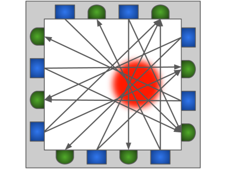
Now consider multiple such terminals embedded in the soft volume: depending on their spatial distribution, a single contact event will affect signals between multiple pairs (see Fig. 1). The magnitude change of all these signals contains information about the contact. A key aspect to extract as much information as possible from this configuration is to measure all possible terminal pairs: a single terminal can be measured against many others. This rich data set can then be mined in purely data-driven fashion to learn the mapping between these signals and the contact parameters of interest. Because each pair of sensing terminals has its own spatial receptive field within the active sensing area and these receptive fields overlap, we call this general method spatially overlapping signals. If the mapping is learned based strictly on collected data, we do not require exact knowledge of terminal locations within the sensor; we simply require that overlapping pairs provide coverage of the intended sensing area (we quantify the impact of coverage on performance later in the paper).
Our method can be summarized into three key ideas, which are also the main contributions of this paper:
-
•
Relatively few terminals can give rise to many terminal pairs, and measuring signal change between all these pairs provides a very rich data set characterizing touch.
-
•
We can use data-driven methods to directly learn the mapping between this rich signal set and our variables of interest, such as the location and depth of an indentation on the surface of the sensor. There is no need for complex models of the material properties or material deformation.
-
•
This approach is general enough to apply to multiple underlying transduction mechanisms. We demonstrate it here with two such methods, based on piezoresistance and optics.
As we will detail in this paper, our method achieves spatial accuracy in the order of 1 mm and less than 1 mm for depth accuracy. This is done using few sensing terminals, which in turn reduces the number of wires needed. We make no assumptions about the underlying sensor geometry, and do not require precise terminal positioning inside the sensor. As a result, the sensors presented in this paper can be manufactured at a very low cost, and do not require complex electronics for signal processing or for the sensing terminals themselves. These characteristics make this method a good candidate to be integrated into robot hands exhibiting complex 3D geometry, which is our directional goal.
Initial versions of the work presented here on the design and performance of the resistive and optical sensors respectively have appeared in conference proceedings: [2, 3]. In this study, we show a significant new capability: discriminating between multiple indenter tips, each with a different shape. More importantly, we show that our data-driven method still allows us to localize touch and determine the depth of indentation accurately for an indenter geometry that the sensor has not been trained on. To achieve this, we introduce a second version of our optical sensor, using surface-mounted components, which increases robustness to drift and allows us to diversify terminal placement. Finally, we also investigate how the number and distribution of sensing terminals affects performance, and how our approach scales to larger sensors.
II Related Work
Numerous types of transduction principles have been explored during the last two decades when building tactile sensors. We refer the reader to a number of comprehensive reviews: [1, 4, 5] for an overview of these methods. Our goal however is not to explore a new sensing modality; rather, we are looking to build on top of such methods, in order to provide continuous sensing with high accuracy without sacrificing manufacturability.
Regardless of the base transduction principle, attempts to increase spatial resolution have often resulted in the arrangement of multiple discrete sensors into a matrix to cover a given target surface. Kane et al. [6], Takao et al. [7] and Suzuki et al. [8] have reported sensor arrays that can develop very high spatial resolution. However, a drawback of this approach is the difficulty involved in manufacturing these arrays onto a flexible substrate than can conform to complex surfaces. Shimojo et al. [9] and Kim et al. [10] present possible technologies to overcome this problem like organic FETs/thin film transistors realized on elastomeric substrates and other related techniques. Still, wiring and manufacturing complexity, along with other system-level issues such as addressing and signal processing of multiple sensor elements, remain important roadblocks on the way to building complete sensing systems.
Electric impedance tomography (EIT) is used to estimate the internal conductivity of an electrically conductive body by virtue of measurements taken with electrodes placed on the boundary of said body. While originally used for medical applications, EIT techniques have been applied successfully for manufacturing stretchable, sensitive skin for robotics that can be deployed on complex surfaces (see [11, 12, 13, 14]). A comprehensive survey on the use of EIT for robotic skin can be found in the work of Silvera et al. [15].
EIT skins are one of the few methodologies to offer stretchable, continuous tactile sensing with the ability to discriminate multiple points of contact with force sensing. Like EIT, we also combine signals from multiple emitter-receiver pairs. However, EIT methods require an analytical model for the internal conductivity to construct an image showing the areas where strain is applied. In contrast, our approach is completely data-driven and does not require the knowledge of a forward model of the sensor. This is what allows us to formulate this method in a general, transducer-agnostic fashion, which in turn can allow the use of transduction methods that are easy to manufacture, but difficult to model analytically. We demonstrate the feasibility and generality of this model-free approach here by using both piezoresistance and light transport as the underlying transduction methods.
An intrinsic advantage of EIT is that it can produce full contact maps for multi-touch situations, an ability which we have not yet investigated with our method. Instead, using our model-free approach, we demonstrate and quantify the ability to very accurately localize single touch (with both a known or unknown indenter), to determine indentation depth, and to discriminate between different indenter shapes. For grasping applications, we believe that the combination of these abilities can prove valuable; for example, when manipulating locally convex objects using fingers with convex links, each link will establish a single contact with the target. In other applications, such full body coverage, where detecting multitouch is a strict requirement, EIT represents a promising alternative.
Our localization approach leverages the overlap of receptive fields in a similar fashion to methods such as super-resolution and electric impedance tomography. van den Heever et al. [16] used a similar algorithm to super-resolution imaging, combining several measurements of a 5 by 5 force sensitive resistors array into an overall higher resolution measurement. Lepora and Ward-Cherrier [17] and Lepora et al. [18] used a Bayesian perception method to obtain a 35-fold improvement of localization acuity (0.12mm) over a sensor resolution of 4mm. In general, super-resolution techniques for tactile sensing leverage overlapping receptive fields of neighboring taxels to perceive stimuli detail finer than the sensor resolution. In this context the sensor resolution relates to the spacing between taxels. While our approach also leverages the overlap of receptive fields, in our case there is no obvious resolution metric for the sensor, since our signals are not the result of an individual taxel, but of a terminal pair whose receptive field is determined by the pair location.
Other sensors also use a small number of underlying transducers to recover richer information about the contact. For example, work in the ROBOSKIN project showed how to calibrate multiple piezocapacitive transducers [19], used them to recover a complete contact profile [20] using an analytic model of deformation, and finally used such information for manipulation learning tasks [21]. Our localization method is entirely data driven and makes no assumptions about the underlying properties of the medium, which could allow coverage of more complex geometric surfaces. Hosoda et al. [22] built an anthropomorphic soft finger with randomly distributed strain gauges and PVDF (polyvinylidene fluoride) films to discriminate between five materials by pressing and rubbing them. This study shares a similar vision to ours because it relies on embedded sensing terminals inside a soft volume, but the authors did not explore the possibility of localizing touch or measuring the contact force. A human operator chooses which pairs carry relevant information and then perform an analytical study of the signal variance to achieve the material classification instead of a learning approach.
The basic building block for one of the sensors presented here is an elastomer with dispersed conductive fillers applied to achieve piezoresistive characteristics. Chortos and Bao [23], Dusek et al. [24] and Kim et al. [25] are just some examples in the literature of this methodology, with carbon black and carbon nanotubes as the most commonly employed fillers. Mannsfeld et al. [26], Park et al. [27] and Wu et al. [28] have shown that multi-layered designs or additional microstructures can further improve performance. Park et al. [29] and Vogt et al. [30] reported that embedding microchannels of conductive fluids inside an elastic volume can be an effective alternative to making the entire volume conductive, especially if large strains are desirable. Here however we opt for the simplicity of single volume isotropic material which can be directly molded into the desired shape. The use of conductive fillers dispersed on elastomers has previously been used to develop tactile sensors. Charalambides et al. [31] used carbon infused PDMS to develop a 3-axis MEMS tactile sensor, using capacitance to measure the deformation of carefully designed pillars.
The other sensors presented in this paper use light transport through an elastomer as a transduction method. The use of optics for tactile sensing is not new, and has a long history of integration in robotic fingers and hands. Early work by Begej [32] demonstrated the use of CCD sensors recording light patterns through a robotic tip affected by deformation. More recently Lepora and Ward-Cherrier [17] showed how to achieve super-resolution and hyperacuity with CCD-based touch sensors integrated into a fingertip. Schneider et al. [33] used color-coded 3D geometry reconstruction to retrieve minute surface details with an optics-based sensor. These studies share a common concept of a CCD array imaging a deformed fingertip from the inside, requiring that the array be positioned far enough from the surface in order to image the entire touch area. In our optic sensor, the sensing terminals are fully distributed, allowing for coverage of large areas and potentially irregular geometry. Additionally, we take advantage of multiple modes of light transport through an elastomer to increase the sensitivity of the sensor. In recent work, Patel et al. [34] took advantage of reflection and refraction to build an IR touch sensor that also functions as a proximity sensor. Their work however does not provide means to also localize contact. Work by Polygerinos et al. [35] uses the deformation of an optic fiber to create a force transducer. This approach has the advantage that the sensing electronics do not have to be located close to the contact area. A very similar sensor exploiting the same physical principles was presented by Levi et al. [36] using an algorithm similar to tomographic back-projection to reconstruct the surface deformation. Our method is completely data driven and takes advantage of two different light transport modes. While their work reports a superior sensitivity to light contact, they do not present any accuracy data in terms of contact localization.
We rely on data-driven methods to learn the behavior of our sensors; along these lines, we note that machine learning for manipulation based on tactile data is not new. Wong et al. [37] learned to discriminate between different types of geometric features based on the signals provided by a previously developed multimodal touch sensor by Wettels et al. [38]. Current work by Wan et al. [39] relates tactile signal variability and predictability to grasp stability using recently developed MEMS-based sensors by Tenzer et al. [40]. With traditional tactile arrays, Dang and Allen[41] successfully used an SVM classifier to distinguish stable from unstable grasps in the context of robotic manipulation using a Barrett Hand. Silvera-Tawil [42] managed to classify six different touch gestures on an experimental EIT-based skin. In contrast, we apply data-driven methods to learn a model of the sensor itself and believe that developing the sensor simultaneously with the learning techniques that make use of the data can bring us closer to achieving complete tactile systems.
III Spatially Overlapping Signals
Our approach begins with a continuous volume of soft material. We use Polydimethylsiloxane (PDMS), a widely used silicon-based organic polymer. It is optically clear and its stiffness can be adjusted by changing the the ratio of curing agent to PDMS. In all sensors presented here we used a ratio of 1:20 curing agent to PDMS by weight.
The spatially overlapping signals methodology is fundamentally based on having multiple pairs of sensing terminals distributed or embedded in the intended sensing area within a given volume of soft material. Generally speaking, a single pair of sensing terminals has a signal associated with it. The signal measured by this sensing pair needs to be sensitive to applied mechanical strain on the underlying material.
A given sensing pair has an associated receptive field or area of influence. Applying mechanical strain within this area will produce a measurable change in the signal for that particular sensing pair. We embed and distribute multiple such sensing terminals within the soft material, so that the intended active sensing area is covered with the receptive fields of multiple sensing pairs. These receptive fields will typically overlap each other, hence a single contact event will have an effect on more than one sensing pair signal (Fig. 1).
To maximize the data extracted we use an all-pairs approach, where all possible sensing terminals pairs are used. This allows us to obtain a very rich data set with few sensing terminals, resulting in a reduced number of wires for the overall sensor. The number of sensing pairs (and thus signals we harvest) is generally quadratic in the number of terminals. This rich data set lends itself to the use of data-driven techniques to directly learn the mapping between the signal set extracted from the sensor and our variables of interest.
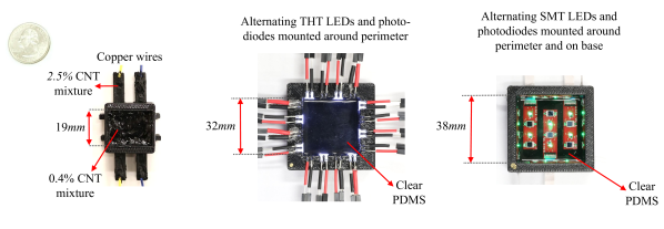
The spatially overlapping signals concept itself is transparent when it comes to the sensing transduction method used. In this paper we show this concept applied with two very distinct transduction methods: resistivity and optics. It must be noted that how we construct these sensing pairs varies depending on the transduction method. In our resistive sensor (Fig. 2, Left), the sensing terminal is simply an electrode and we can match a given terminal with any other to measure resistance. However in the case of our optical sensors (Fig. 2, Middle and Right), a given sensing terminal has a defined role: it can either be an emitter (an LED) or a receiver (a photodiode). An immediate consequence of this fact is that the number of sensing pairs as you add a sensing terminal grows slower for our optical sensors than for the resistive sensor (though the number of pairs is still quadratic in the number of terminals in both cases). Moreover, the resistive sensor only requires one wire per sensing terminal, compared to the two wires required on the optical sensors for each LED and photodiode.
One of the trade-offs in our method is that of data processing. Building an analytical model of how this rich signal set is affected by contact characteristics is a daunting task; furthermore, any such model would depend on knowing the exact locations of the terminals in the sensor, thus requiring very precise manufacturing. Qualitatively, we expect that the intensity of the collected signals is directly related to the location and magnitude of the applied strain.
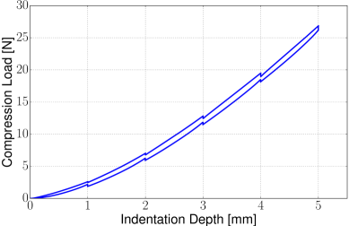
We thus use a purely data-driven method to directly learn the mapping between the signal set extracted from the sensor and our variables of interest. We train our method using a set of indentations of known characteristics. In particular, in this paper we focus mainly on learning a mapping for contact localization and indentation depth. Throughout this study we use indentation depth as a proxy for contact force; for conversion to force values, we provide the stiffness curve of our constituent material in Fig. 3. Using an optical sensor, we also investigate the ability to discriminate between a finite set of possible indenter shapes. We do not discard the possibility of learning more contact parameters in the future.
In the following sections, we present concrete implementations of these concepts using two transduction methods, based on resistance and optics respectively. For each prototype (one using resistance and two using optics) we present our manufacturing methods, data collection protocol, and results analysis.
IV Resistivity based sensor
When applying the spatially overlapping signals method with piezoresistance as the underlying transduction method, the sensor consists of a single continuous volume of piezoresistive polymer with a number of embedded electrodes (Fig. 2, Left).
IV-A Sensor manufacturing
To achieve piezoresistance for our silicone, we disperse multiwall carbon nanotubes (MWCNT, purity: 85%, Nanolab Inc.) into PDMS (Sylgard 184, Dow Corning). The key aspect for this procedure is choosing the appropriate ratio of conductive filler to elastomer. According to the percolation theory, a composite will display the most pronounced piezoresistive effect for a ratio referred to as the percolation threshold by Hu et al. [43]. In order to find this value for our materials, we tested a series of samples with the concentrations of MWCNTs from 0.2wt.% to 5wt.%. We found that the most pronounced change in conductivity occurred around the threshold of 0.4wt.% filler, which we used in all subsequent experiments.
In order to achieve uniform distribution of carbon nanotubes within PDMS, we use chloroform as a common solvent, an approach referred to as the solution casting method by Liu and Choi [44]. First, we combine chloroform and MWCNT and use a horn-type ultrasonicator in a pulse mode with 50% amplitude for 30 min to evenly disperse the MWCNTs. Then we add PDMS to the mix (at chloroform:PDMS weight ratio of 6:1 or more to reduce the viscosity of the mixture), stir for 5 min to diffuse the PDMS, and then sonicate again for 30 min. We then heat the mixture at 80∘C for 24 hours to evaporate the chloroform. After adding the curing agent, the mixture is ready to be poured into the mold; for the experiments presented here we empirically selected a curing agent to PDMS ratio of 1:20. Finally, the sample is cured in an oven at 80∘ C for 4 hours.
In order to isolate piezoresistive effects from mechanical changes at the contacts due to indentation, we mechanically separated the wire contacts from the piezoresistive sample placed under indentation tests. We extended a number of 30mm side channels from the sample, each filled with a CNT-filled PDMS mixture with a higher concentration of 2.5wt.% We then embedded copper wires directly into the mixture at the end of these channels (Fig. 2, Left). The mixture with the ratio of 2.5wt.% has no piezoresistive characteristics and its conductivity is close to that of the copper wires; thus, the mixture with the ratio of 0.4wt.% located at the center of the mold dominates the overall conductivity.
Our sampling circuit measures the change in resistance between all pairs of terminals that occurs as a result of some strain being applied to our sample material. For each one of our six terminal pairs, we take a baseline resistance measurement. This value is then compared against the real time measurement after strain is applied using an instrumentation amplifier. The amplified signal is directly fed to an analog to digital converter. A switching matrix scheme allows us to quickly perform this procedure on all six sensing pairs. The overall circuit delivers the set of all six measurements every 25 milliseconds, resulting in a 40Hz sampling frequency.
IV-B Data collection
We collect training and test data with a planar stage (Marzhauser LStep) and a linear probe located above the stage to indent vertically on the sensor with a 6mm hemispherical tip. The probe is position-controlled and the reference level is set manually such that the tip barely makes contact with the sensor. The probe does not have force sensing capability, hence we use indentation depth as a proxy for indentation force.
For indentation locations, we use two patterns. The grid indentation pattern consists of a regular 2D grid of indentation locations, spaced 2mm apart along each axis. However, the order in which grid locations are indented is randomized. This is in contrast with the random indentation pattern, where the locations of the indentations are sampled randomly over the surface of the sample. The grid indentation pattern is used for training our algorithms, while the random indentation pattern is used as a test set.
Taking into account the tip diameter, plus a 1mm margin such that we do not indent directly next to an edge, our regular indentation pattern results in 54 indent locations distributed over a 10mm by 16mm area (9x6 grid).
For each indentation location, we sample the signal from each pair of electrodes at a depth of 3mm. Each such measurement results in a tuple of the form , where and represent the location of the indentation, is the indentation depth, and (also referred to collectively as ) represent the change in the six resistance values we measure between depth and depth 0 (the probe on the surface of the sample). These tuples are used for data analysis as described in the next section.
IV-C Analysis and results
Our first goal is to learn the mapping from all terminal pairs readings to the indentation location . To train the predictor, we collected four data sets in regular grid patterns, totaling 216 indentations (9x6 grid, hence each set contains 54 indentations) . For testing, we collected a dataset consisting of 60 indentations in a random pattern. All indentations were performed to a depth of 3mm, or 50% of the total depth of the sample. The metric used to quantify the success of this mapping is the magnitude of the error (in mm) between the predicted indentation position and ground truth. In our analysis below, we report this error for individual test points, as well as its mean, median and standard deviation over the complete testing set.
The baseline that we compare against includes a “Center Predictor” and a “Random Predictor”. The former always predicts the location of the indentation on the center of our sample, and the later predicts a completely random location within the sample surface. The useful area of our sample is 16mm by 10mm; on our test set, the Center Predictor produces a median error of 5mm, while the random predictor, if given a large test set, converges on a median error of above 6mm.
We first attempted Linear Regression as our learning method. The results were significantly better than the baseline, with a median error of under 2mm. Still, visual inspection of the magnitude and direction of the errors revealed a circular bias towards the center that we attempted to compensate for with a different choice of learning algorithm. The second regression algorithm we tested was Ridge Regression with a Laplacian kernel. The Laplacian kernel is a simple variation of the ubiquitous radial basis kernel, which explains its ability to remove non-linear bias. In this case, we used the first half of the training data for training the predictor, and the second half to calibrate the ridge regression tuning factor and the kernel bandwidth through grid search.
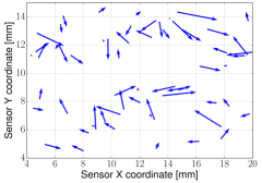
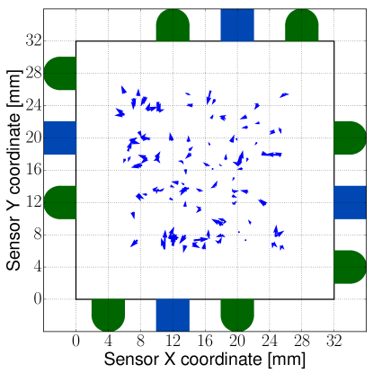
The numerical results using both of our predictors, as well as the two baseline predictors, are summarized in Table I. These results are aggregated over the complete test set consisting of 60 indentations. Linear regression identifies the location of the indentation within 2mm on average, while Laplacian ridge regression (, ) improves these results to sub-millimeter median accuracy. In addition to the aggregate results, Fig. 4 illustrates the magnitude and direction of the localization error for the ridge regression.
| Predictor | Median Err. | Mean Err. | Std. Dev. |
|---|---|---|---|
| Center predictor | 5.00 mm | 5.13 mm | 2.00 mm |
| Random predictor | 6.30 mm | 6.70 mm | 3.80 mm |
| Linear regression | 1.75 mm | 1.75 mm | 0.83 mm |
| Lapl. ridge regr. | 0.97 mm | 1.09 mm | 0.59 mm |
IV-D Discussion and limitations
Our results with the piezoresistive sensor illustrate both the advantages and the downsides of this transduction method. Considering first the positive features, we note that any terminal can act as both emitter and receiver, and any terminal requires a single wire. As such, this method has the potential to provide a very rich data set with very few wires. This is illustrated by our sensor, which achieves sub-millimeter localization accuracy over a area with only four total wires.
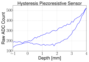
However, we have also found a number of limitations that could not be avoided using our manufacturing techniques. The mechanical interface between the terminals and the piezoresistive elastomer significantly affects resistance measurements; in this proof-of-concept prototype, we used side channels with highly conductive elastomer to isolate the sensor, but this complicates future integration in robot fingers. We also found that the sensor exhibits significant hysteresis over time scales on the order of seconds, as well as signal drift over longer time scales (days). Fig. 5, Left shows the resulting signal from a particular terminal pair during a controlled indentation event. We mitigate this here by using the resistance values at depth 0 (just before touching) as a baseline that is subtracted from all signals collected during that indentation, and by always indenting to a known depth, but these methods again limit future applicability to robot hands.
We believe that overlapping piezoresistive signals are worth considering, as they hold significant promise for collecting rich data with very few terminals, with additional improvements needed in the manufacture of piezoresistive elastomers with embedded electrodes. In this study, we now move to a different transduction method based on optics, where we trade off an increase in wire count (and thus complexity) for a much simpler manufacturing method and improved SNR which yields greatly improved performance and the ability to predict depth.
 |
 |
V Optics based sensor
When using optics as a transduction method, our sensor consists of a continuous volume of optically clear elastomer, with embedded light emitters and receivers. The first version we describe has emitters and receivers only along the perimeter of the sensing area (Fig. 2, Middle); in the next section we will consider a version with terminals also embedded on the base.
An important difference compared to the piezoresistive sensor is the fact that now our sensing terminals have defined roles as either an emitter (LED) or a receiver (photodiode). The all-pairs approach still applies; we pair each emitter with all possible receivers. Note that in this paper we will refer to both an LED or photodiode as a “sensing terminal”.
V-A Light transport and interaction modes
We first focus on a single emitter-receiver pair in order to discuss the underlying light transport mechanism in detail. The core transduction mechanism relies on the fact that as a probe indents the surface of the sensor, light transport between the emitter and the receiver is altered, changing the signal reported by the receiver (Fig. 6). Consider the multiple ways in which light from the LED can reach the opposite photodiode: through a direct path or through a reflection. In particular, based on Snell’s law, due to different refractive indices of the elastomer and air, light rays hitting the surface below the critical angle are reflected back into the elastomer.
|
|
 |
 |
As the probe makes initial contact with the sensor surface, the elastomer-air interface is removed from the contact area and surface normals are immediately disturbed. This changes the amount of light that can reach the diode via surface reflection. This is the first mode of interaction that our transduction method captures. It is highly sensitive to initial contact, and very little penetration depth produces a strong output signal.
As the depth of indentation increases, the indenter starts to also block light rays that were reaching the photodiode through a direct, line-of-sight path. This is our second mode of interaction. To produce a strong signal, the probe must reach deep enough under the surface where it blocks a significant part of the diode’s surface from the LED’s vantage point.
We note that other light paths are also possible between the emitter and receiver. The interface between the clear elastomer and the holding structure (the bottom and side walls of the cavity) can also give rise to reflections. While we do not explicitly consider their effects, they can still produce meaningful signals that are captured by the data-driven mapping algorithm.
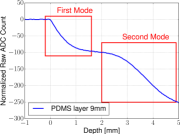
We would like our sensor to take advantage of both operating modes described above, noting that one is highly sensitive to small indentations while the other provides a strong response to deeper probes. We thus aim to design our sensor such that these two modes are contiguous as the indentation depth increases. The goal is to obtain high sensitivity throughout the operating range of the sensor. The key geometric factor affecting this behavior is the height of the elastomer layer, which we determine experimentally.
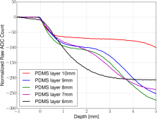
To investigate this factor, we constructed multiple 3D printed square molds with LEDs (SunLED XSCWD23MB) placed 20mm in opposition from the photodiode (Osram SFH 206K), with PDMS filling the cavity. Work by Johnson and Adelson [45] shows PDMS and air have approximate refractive indexes of 1.4 and 1.0 respectively, with a critical angle of degrees. Each mold was filled with PDMS to achieve a different layer thickness and then indented to 5mm depth in a midpoint location between the LED and the photodiode. Results are shown in Fig. 6. We note that prototypes with PDMS layers over 10mm exhibited a dead band: after a certain threshold depth the photodiode signal does not change as we indent further down until you indent deep enough to activate the second mode. In contrast, the 7mm layer provides the best continuity between our two modes, while the 8mm layer gives good continuity while also producing a stronger signal when indented. We thus built all our subsequent sensors with an 8mm PDMS layer.
V-B Sensor manufacture
We validate this concept on a sensor comprised of 8 LEDs and 8 photodiodes arranged in an alternating pattern and mounted in sockets along the central cavity walls. For this sensor we used through-hole technology (THT) components for ease of prototyping. We used a 5mm x 5mm x 7.2mm sized LED model SunLED XSCWD23MB with peak wavelength 460nm and a Osram SFH 206K photodiode with peak sensitivity at 850nm and a 2.65mm x 2.65mm sensitive area. To build the sensor we use a 3D printed square mold with exterior dimensions of 48mm x 48mm. The cavity in the mold is 32mm x 32mm. Any LED is thus able to excite multiple photodiodes.
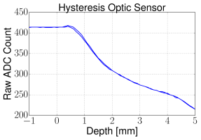
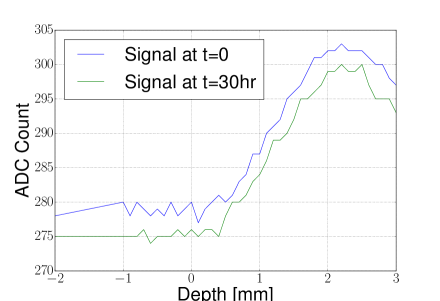
As this sensor only has terminals around its perimeter, the base simply consists of 3D printed ABS plastic. However, we found that the clear elastomer and the holding plastic exhibit bonding/unbonding effects at a time scale of 5-10s when indented, creating unwanted hysteresis. To eliminate such effects, we coat the bottom of the sensor with a 1mm layer of elastomer saturated with carbon black particles (shown in Fig. 6 by a thick black line). This eliminates bottom surface reflections, and exhibits no adverse effects, as the clear elastomer permanently bonds with the carbon black-filled layer. As shown in Fig. 5, this sensor exhibits little to no hysteresis between an indentation and the subsequent retraction, in contrast to the resistive version.
An Arduino Mega 2560 handles LED switching and taking analogue readings of each photodiode. The photodiode signal is amplified through a standard trans-impedance amplifier circuit, and each LED is driven at full power using an NPN bipolar junction transistor. The resulting sampling frequency with this setup is 60Hz.
V-C Data collection
When collecting data, we read signals from all the photodiodes as different LEDs turn on. Having 8 LEDs gives rise to 8 signals for each photodiode, plus an additional signal with all LEDs turned off for a total of 9 signals per diode. This last signal allows us to measure the ambient light captured by each diode and subtract it from all other signals, so that the sensor can perform consistently in different lighting situations.
The main difference compared to the piezoresistive sensor is that we treat indentation depth as an additional variable. At each location we use the following protocol. We consider the sensor surface to be the reference level, with positive depth values corresponding to the indenter tip going deeper into the sensor. We collect data at both negative and positive depths. For depths between and , we collect one data point every . The indenter then goes down to a depth of taking measurements every . The same procedure is mirrored with the indenter tip retracting.
Each measurement results in a tuple of the form where is the indentation location in sensor coordinates, is the depth at which the measurement was taken and correspond to readings of our 8 photodiodes as we turn each LED on: state , from which we subtract the ambient light captured by each diode when all LEDs are turned off (state ). We thus have a total of 75 numbers in each tuple .
Similar to the previous sensor, we use a grid indentation pattern for training data and a random indentation pattern for testing. Taking into account the diameter of our tip, plus a 3mm margin such that we do not indent directly next to an edge, our grid indentation pattern results in 121 locations distributed over a 20mm x 20mm area (11x11 grid). We allow for a bigger margin compared to the resistive sensor since the components are mounted directly on the walls of our mold.
V-D Analysis and results
Our objective here is to learn the mapping between our photodiode readings for to the indentation location and depth . Note that the ambient light measurement (state ) is not used as a feature, since it has already been subtracted from other states.
To train our predictors we collected four grid pattern datasets, each consisting of 121 indentations, and each indentation containing 161 datapoints at different depths. Aiming for robustness to changes in lighting conditions, two of these datasets were collected with the sensor exposed to ambient light and the other two datasets were collected in darkness. The feature space used for training has a dimensionality of 64. For testing, we collected two datasets using the random indentation pattern, one collected in ambient light and another collected in the dark, with 100 indentation events in each.
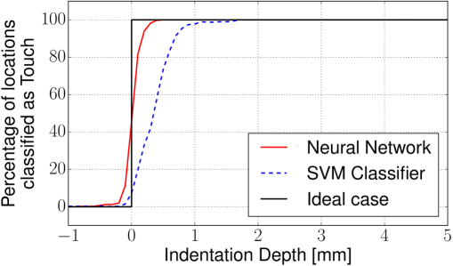
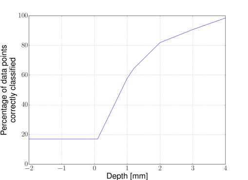
Touch classification. The first step we take is to use a classifier to determine if touch is occurring; this classifier is trained on both data points with and . We tested two different classification methods: a linear SVM and a Neural Network (NN) with one input layer, one hidden layer (1024 nodes, ReLU activation function) and one output layer (1 node, sigmoid activation function). Results for both classifiers are presented in Fig. 7. For any given depth, we show the percentage of indentations (over all of our test locations) that are classified as touch.
For an indentation depth of 0.1 mm the NN classifier correctly classifies 82% of the events as “touch”, increasing to 94% at 0.2 mm and hitting 98% at 0.3 mm. The price we pay is an 11% misclassification rate at -0.1 mm depth (slightly above the surface). The SVM classifier rarely interprets cases above the surface as touch, but starts reliably predicting touch (above 80% of cases) at a depth of 0.5 mm or higher, hitting 99% after 1 mm. Overall, using the NN classifier, and according to the elasticity profile shown in Fig. 3, we detect touch with 82% reliability for a force of 0.11 N (0.1 mm indentation) and 98% reliability at 0.55 N (0.3 mm) or higher.
Depth and location regression. If the classifier predicts touch is occurring, we use a second stage regressor to predict values for . This regressor is trained only on training data with . We use a kernelized ridge regressor with a Laplacian kernel and use half of the training data to calibrate the ridge regression tuning factor and the kernel bandwidth through grid search. However, the computational requirements of training a ridge regressor with a non-linear kernel require downsampling of our training data: for each indentation, we only trained on indentation depths in 0.5 mm increments starting from the surface of the sensors. Results presented in this section were obtained with and .
| Ambient Light Dataset | |||||||||||||||||||||||||||||||||||||||||||||||||||||||||||||||
|
|||||||||||||||||||||||||||||||||||||||||||||||||||||||||||||||
| Dark Dataset | |||||||||||||||||||||||||||||||||||||||||||||||||||||||||||||||
|
|||||||||||||||||||||||||||||||||||||||||||||||||||||||||||||||
 |
 |
 |
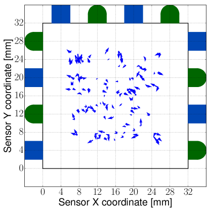
| Center | Edge | Corner |
 |
 |
 |
|
 |
 |
The metric used to quantify the success of our regressor is the magnitude of the error for both the localization and depth accuracy. Detailed numerical results for both of these metrics, and for both ambient light and dark datasets, are presented in Table II, aggregated over our entire test sets.
To provide more insight into the behavior of the sensor, we present additional visualizations for the error in both depth and location. The results for depth can only be visualized for specific locations. Fig. 8 shows the performance at three different locations in our ambient light test dataset. Since this regressor is trained only on contact data, it is not able to predict negative depths which causes error to be greater at depths close to 0mm. At 0.5mm and deeper, the depth prediction shows an accuracy of below half a millimeter.
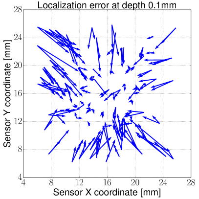
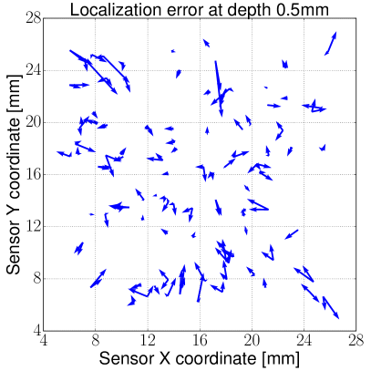
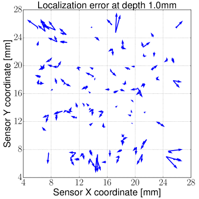
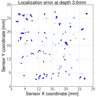
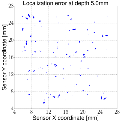
Localization results on the light dataset can be visualized in Fig. 9 for a few representative depths. At depth 0.1mm the signals are still not good enough to provide accurate localization, but as we indent further down localization improves well beyond sub-millimeter accuracy.
Signal removal analysis. Given the nature of our spatially overlapping signals method, it is of special interest to analyze the relationship between the number of sensing terminals and the resulting accuracy in touch localization and depth prediction. Our hypothesis is that a higher number of sensing terminals will yield higher accuracy, but how we distribute these terminals to over the intended sensing area also plays an important role in determining performance.
We consider four different cases for our optical sensor. In each case, we discard the signals from a subset of terminals of the base configuration (which has a total of 16 terminals). We compare these cases between themselves, and against the base configuration. We use the localization and depth error at a depth of 2mm for the sake of readability (other depths follow the same trend).
 |
 |
| (a) Case 1 | (b) Case 2 |
 |
 |
| (c) Case 3 | (d) Case 4 |
| Cases | Localization Error (mm) | Depth Error (mm) | ||||
|---|---|---|---|---|---|---|
| Median | Mean | Std Dev | Median | Mean | Std Dev | |
| Basel. | 0.42 | 0.50 | 0.31 | 0.04 | 0.04 | 0.03 |
| Case 1 | 0.62 | 0.69 | 0.41 | 0.06 | 0.08 | 0.07 |
| Case 2 | 0.70 | 0.80 | 0.49 | 0.11 | 0.13 | 0.11 |
| Case 3 | 0.86 | 1.02 | 0.67 | 0.12 | 0.15 | 0.11 |
| Case 4 | 1.11 | 1.24 | 0.75 | 0.17 | 0.21 | 0.17 |
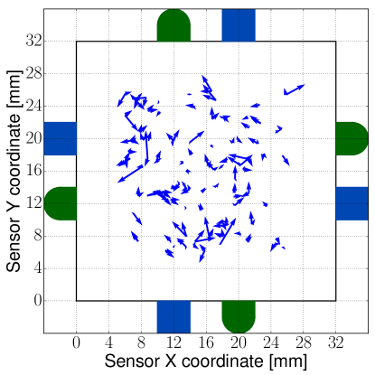
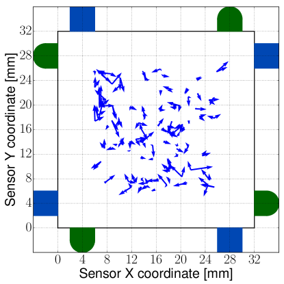
The four cases are presented in Fig. 10. Cases 1 and 2 have four sensing terminals removed (4 LEDs in Case 1, 2 LEDs and 2 photodiodes in Case 2). However, they present different distribution of terminals along the edge of the sensing area. Cases 3 and 4 each have eight terminals removed (4 LEDs and 4 photodiodes), again with different spatial distributions. Localization results are also shown in Fig. 10. (Comparative performance for the base case is in Fig. 9 at 2mm depth.) Accuracy in both localization and depth predictions is also summarized in Table III.
Results show that a higher number of sensing terminals always results in a lower median error for localization accuracy and for depth accuracy. Additionally, we make two observations on this data. First, performance tends to increase or decrease uniformly, over the entire surface of the sensor, rather than locally, in the vicinity of additional terminals. Case 2 shows no noticeable difference in performance along the top vs. bottom edges; Cases 3 and 4 do not differentiate between corners and edge centers despite different terminal placements.
Second, for the same number of terminals, a more homogeneous distribution uniformly increases general performance. Numerical results show that case 1 performs better than case 2 in both metrics with the same number of sensing terminals, but with a more homogeneous distribution of the receptive fields for the sensing pairs. Following the same pattern, case 3 also outperforms case 4. Both of these phenomena could be due to the fact that our intuition with respect to how the light travels through the elastomer and what the receptive fields for a given pair look like might be a bit too simplistic. As that we rely of a purely data driven method, all of these complex interactions are captured at training time. Future studies can provide more insight as to how to optimize the distribution of the sensing terminals to aid the design of our sensors.
Multistage training for larger sensors. An important question regarding our approach is its ability to scale to larger sensor sizes. With our current geometry, increasing the dimension of the sensor side leads to a proportional increase in the distances between sensing elements (as long as they are still distributed only on the border), and a quadratically increased sensing surface area.
To investigate these effects, we constructed a second optical sensor with a 45 mm side. Accounting for the tip diameter and the safety margin (as before), this implies a 1024 mm2 sensing area, a 2.56X increase compared to the sensor shown in Fig. 2, Middle. All other aspects of the design where unchanged, including the number of terminals and their distribution in the sensor.
We applied the exact same data-driven mapping algorithm described in the previous section. We recall that the core learning algorithm used is an kernel ridge regressor trained to simultaneously predict indentation depth and location. We thus refer to this method as “single-stage training”; the results on the larger sensor are shown in Table IV. As expected, we notice a performance degradation compared to the smaller sensor, even though localization error is still below 1 mm at indentation depths of 2 mm or higher.
| Depth | Single stage training | Multistage training | ||||
|---|---|---|---|---|---|---|
| (mm) | Median | Mean | Std. Dev | Median | Mean | Std. Dev |
| 0.1 | 2.22 | 2.63 | 1.87 | 1.72 | 2.15 | 1.65 |
| 0.5 | 1.67 | 1.95 | 1.29 | 1.27 | 1.48 | 1.03 |
| 1.0 | 1.36 | 1.50 | 0.92 | 1.17 | 1.32 | 0.84 |
| 2.0 | 0.94 | 1.06 | 0.64 | 0.53 | 0.68 | 0.43 |
| 3.0 | 0.74 | 0.81 | 0.47 | 0.63 | 0.75 | 0.49 |
| 5.0 | 0.94 | 1.06 | 0.64 | 0.53 | 0.60 | 0.38 |
One possibility to recover some of the performance drop would be to increase the amount of training data; however, given the larger surface size, this becomes prohibitively expensive from a computational standpoint if training a single regressor. To account for this, we split our training / testing procedure into specialized stages. First, we trained an linear regressor to exclusively predict the depth of the indentation. Second, we used five separate regressors to predict indentation location, each trained for specific range of depths. Each of these regressors was trained on a 1 mm slice of indentation depths, centered at 0.5, 1.5, 2.5, 3.5 and 4.5 mm respectively.
The corresponding multistage testing procedure is as follows: first, the specialized depth regressor predicts indentation depth, referred to as . Then, based on this result, the test tuple is sent to the localization regressor whose range covers . In turn, this chosen regressor predicts the location of the indentation, which completes our prediction.
The advantage compared to single-stage prediction is that each localization regressor is only trained on a subset of the data - the slice corresponding to its assigned depth range. We can thus afford to increase the resolution of our training samples by a similar amount with no effect on the training time. Taking advantage of this, we trained our predictors using training data sampled at every 0.1 mm in depth (as opposed to 0.5 mm in the previous section). The results of this multistage approach (with more training data) are also shown in Table IV.
We notice that adding more training data increases performance at all depths and approaches the results obtained for the smaller sensor. Overall, we believe these results show that our approach can scale to larger sensor sizes, and that training variants that allow for more data can, up to a point, help mitigate performance loss. Of course, if the sensor size keeps increasing, we expect to run into computational limits that could require a completely different learning approach. However, we believe that the dimensions demonstrate here are in line with the requirements of our desired application, integration into robot fingers for human-scale manipulation.
V-E Discussion and limitations
The perimeter-based THT optical sensor combines sub-millimeter localization accuracy (in many cases improving to half-millimeter) with indentation depth determination within a tenth of a millimeter. Still, these results have all been obtained with a single indenter tip, used for both training and testing, and do not speak to the abilty to handle different indenter shapes.
 |
 |
Additionally, we have found that these sensors, while showing no discernible hysteresis over time scale on the order of seconds, do exhibit signal drift over periods of hours and large numbers of repeated indentations (Fig. 11, Left). Visual inspection showed that, after repeated indentations and over long periods of time, the transparent elastomer begins detaching from the surface of the LEDs, which affects light propagation. We address both of these aspects with a second version of our sensor, described in the next section.
VI Surface-mount optical sensor with base terminals
For the second iteration of our optics-based sensor, we switched from through-hole technology (THT) LEDs and photodiodes to surface-mount technology (SMT) components. We developed prototype boards containing two LEDs and two photodiodes each, with all wiring for the four components combined through a single connector. Compared to using through-hole components, this packaging simplified the manufacturing process for also including terminals on the base of the sensor. This prototype is shown in Fig. 2, Right.
VI-A Sensor manufacture
The SMT optic sensor follows a similar fabrication method to the THT version. We initially 3D print out of ABS plastic a square mold with exterior dimensions of 48mm x 48mm. The interior cavity in the mold is 38mm x 38mm. This sensor presents sockets both on its walls, as well as on its base to fit the small PCB boards where the LEDs and photodiodes are located.
Each PCB board measures 29mm length and 8mm width. The front of the PCB board holds two 1.6 mm x 0.8 mm LEDs (Kingbright APG1608ZGC, peak wavelength 515nm) and two 4.0mm x 4.5mm photodiodes (OSRAM BPW34S E9601, peak sensitivity 850nm) in alternate pattern. Additionally, the front holds an FFC connector to interface with our measuring circuit. The back of the PCB board holds an operational amplifier (Analog Devices AD8616) on a trans-impedance amplifier configuration. Overall this sensor uses 7 PCB boards, 4 being located on the mold’s walls and the remaining 3 being placed on the mold’s base. This represents a total of 14 LEDs and 14 photodiodes.
For the same reasons as in our THT optic sensor, before installing the PCB boards, we coat the base of the sensor with a 1mm layer of PDMS saturated with carbon black particles. After curing this layer, we cut out the carbon black infused PDMS on the sockets so that we can place the boards inside them. For all PCB boards we use a few drops of glue to place them inside their sockets. The flexible flat cables used to connect to each individual board are routed through small holes on the walls of the 3D printed mold. After connecting each board, these holes are sealed using epoxy. At this point, we fill the mold cavity with the elastomer at a 1:20 curing agent to PDMS ratio.
A microcontroller (NXP LPC1768) handles switching the LEDs and taking analogue readings of each photodiode. The resulting sampling rate to collect and report all signals is approximately 100Hz.
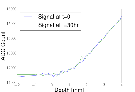
An important result of this manufacturing process is the absence of drift over large time scales and large numbers of intermediate indentations. Fig. 11 shows a comparison of individual signals over time for both versions of the optical sensor. The THT sensor exhibits a clear drift in the signal while the SMT sensor shows no similar phenomenon. We attribute this change to the use of SMT LEDs with much smaller surface area, that do not exhibit unwanted bonding/unbonding behavior with the elastomer.
VI-B Data collection
We collect data on this sensor in the same manner as that presented for the first iteration of our optics-based sensor presented in Section V-C. One difference is that we now use 14 LEDs and 14 photodiodes. We continue to read a baseline signal with all LEDs turned off which we subtract from all other signals to make the sensor robust under changing ambient light conditions. This results in 15 signals for each photodiode.
The primary difference with this sensor is that we now repeat this data collection process for multiple indenter tips. To mimic geometries which are likely to be encountered in common workspaces, we manufactured the following indenter tips: circular planar with diameter, edge with length, and a square corner with maximum width . We take separate data sets with the edge tip oriented at three positions, each apart. We also include the diameter hemispherical tip which was used in previous sections. This results in 6 different indenter tips.
Following the depth convention outlined in Section V-C, we take one measurement at and measurements at intervals between depths of and . We then take a measurement every down to the maximum indendation depth. The process is mirrored on retraction. Due to force constraints on our indentation actuator, every tip does not reach the same maximum indentation depth. The planar tip reaches a maximum depth of , the edge tip reaches a maximum of , and all other tips reach a maximum depth of .
Each measurement now results in a tuple of the form where identifies the tip used for the indentation, is the indentation location in sensor coordinates, is the depth at which the measurement was taken and correspond to readings of our 14 photodiodes as we turn each LED on: state , from which we subtract the ambient light captured by each diode when all LEDs are turned off (state ). We thus have a total of 214 numbers in each tuple .
We again use a grid indentation pattern for training and a random indentation pattern for testing. This sensor has a x PDMS surface. Taking into account our larger tip radius () and a margin, our indentation pattern results in 81 locations distributed in intervals over a x grid. For testing, the random indentation pattern consists of 100 indentation events scattered within the same area.
VI-C Analysis and results
Our objective here is twofold: to determine whether our signals contain sufficient information to reliably classify the tip geometry with which the sensor is being contacted; and to explore our sensor’s ability to identify contact depth and location regardless of tip geometry. To train our models we use a single data set for each tip, each collected in the dark. The feature space for training has a dimensionality of 196.
Discriminating between indenter geometries. To perform this classification we use a Neural Network with one input layer, one hidden layer (1024 nodes, ReLU activation function), and one output layer (6 nodes, softmax activation function). The classifier is trained and tested on all six data sets, with both and . The primary metric for evaluating classifier performance is accuracy; that is, the ratio of the number of data points correctly classified to the total number of data points. This performance is shown as a function of indentation depth in Fig. 13.
In the limit of negative depths, the classification accuracy converges to the expected , or random chance. The accuracy increases with indentation depth and achieves a maximum of at .
Depth and location regression. The goal here is to determine our ability to identify contact location and indentation depth regardless of indenter tip geometry. To do this, we use a kernelized ridge regressor analogous to that presented in Section V-D. We train this regressor on all six datasets. Due to the size of this combined dataset and the computational requirements of training this regressor, we undersample our data based upon depth, maintaining higher granularity near the sensor surface. Results presented in this section were obtained with and . The results of testing this regressor on all six datasets are tabulated in Table V. Compared to the localization and depth regression performance of the optics-based sensor shown in Table II, we see improved performance at low depths and weaker performance at larger depths. However, we consider these results to be well within the operating margin for a practicable sensor.
| Depth | Localization Error (mm) | Depth Error (mm) | ||||
|---|---|---|---|---|---|---|
| (mm) | Median | Mean | Std. Dev | Median | Mean | Std. Dev |
| 0.1 | 1.58 | 1.81 | 1.17 | 0.17 | 0.18 | 0.10 |
| 0.5 | 1.35 | 1.53 | 1.00 | 0.10 | 0.12 | 0.09 |
| 1.0 | 1.13 | 1.38 | 0.95 | 0.10 | 0.13 | 0.10 |
| 2.0 | 0.96 | 1.21 | 0.90 | 0.18 | 0.22 | 0.17 |
| 3.0 | 0.91 | 1.14 | 0.85 | 0.28 | 0.33 | 0.24 |
| 4.0 | 1.11 | 1.27 | 0.78 | 0.63 | 0.66 | 0.32 |
Tip removal analysis. In practice, a tactile sensor will encounter indentation geometries which have not been included in the training of its working model. In pursuit of robustness when faced with such a situation, we analyze our sensor’s performance when testing on tip data not included in training. We train six regressors, each on a different five of the six possible tips. Each of these regressors is then tested exclusively on data associated with the missing tip. The results of this analysis are tabulated in Table VI. Overall, these results are on the same order as those seen when all tips are included (Table V), suggesting the ability of our sensor to accurately predict on indentation geometries not formerly encountered.
| Tip | Localization Error (mm) | Depth Error (mm) | ||||
|---|---|---|---|---|---|---|
| Removed | Median | Mean | Std. Dev | Median | Mean | Std. Dev |
| Planar | 1.30 | 1.31 | 0.61 | 0.18 | 0.21 | 0.17 |
| Edge 1 | 1.27 | 1.32 | 0.56 | 0.61 | 0.58 | 0.24 |
| Edge 2 | 0.97 | 1.10 | 0.66 | 0.29 | 0.29 | 0.19 |
| Edge 3 | 0.61 | 0.80 | 0.59 | 0.16 | 0.18 | 0.13 |
| Corner | 0.90 | 1.05 | 0.66 | 1.08 | 1.08 | 0.10 |
| Hemisphere | 1.10 | 1.36 | 0.91 | 0.51 | 0.51 | 0.11 |
VI-D Discussion
The SMT-based optical sensor adds the important capability to discriminate between different indenter shapes, while maintaining accurate localization and depth determination capabilities. An important characteristic is the lack of discernible hysteresis or drift over time scales ranging from seconds to days, and over large number of indentations. This allows us to collect large data sets with many indenter tips, needed for the tip discrimination.
Along with the new tip discrimination ability, the SMT version also exhibits a slight decrease in localization and depth prediction ability compared to the THT version. We attribute this to the same decreased size of the light emitting terminal: a smaller LED means fewer rays hitting any given receiver, in both interaction modes described in Section V-A. In the limit, if both the emitter and the receiver are reduced to points, both modes become binary, allowing for just an on/off signal, thus reducing the ability to discriminate. A possible compromise could use multiple SMT LEDs, activated together as a unit and in close proximity to each other, to maintain elastomer bonding, but emulate the larger surface area of the THT version.
VII Discussion and Conclusions
In this paper, we explored a data-driven methodology based on multiple pairs of sensing terminals distributed inside a volume of soft material to create tactile sensors. By using an all-pairs approach, where a sensing terminal is paired with every other possible terminal, we obtain a very rich data set using fewer wires. We then mine this data to learn the mapping between our signals and the variables characterizing a contact event. This spatially overlapping signals methodology can be generalized to different transduction methods: here we show sensors based on resistivity and optics using both THT and SMT components.
Our resistive sensor with an effective sensing area of discriminates contact location with sub-millimeter median accuracy for an indentation depth of . Our THT optical sensors achieve sub-millimeter localization accuracy over and workspaces, for indentation depths ranging between and . The SMT optic sensor can localize contacts with an accuracy of approximately regardless of the indenter geometry over a workspace. To achieve similar accuracy, the traditional sensor matrix approach would require numerous individual taxels with complex manufacturing, wiring and addressing techniques. In contrast, we use four terminals (with one wire each) for the resistive sensor, and as few as 16 and 28 terminals (with two wires each) for the THT and SMT optic sensors respectively.
For all of our THT optic sensors, we also show identification of indentation depth accurate to within for a large part of its operating range. We use depth here as a proxy for indentation force, based on a known stiffness curve for our sensor; it is also possible to adjust the PDMS layer thickness and stiffness to affect the sensor sensitivity and dynamic range. A stiffer PDMS layer will require a larger force to activate the second detection mode.
Comparing the two transduction methods presented here, the number of wires required by each sensor is significantly different. A single sensing terminal in the resistive sensor takes one wire, versus two wires needed for an LED or photodiode in the optical sensor. Moreover, the nature of measuring resistance means we can pair a sensing terminal with any other, whereas in the optical sensor case, a pair must be formed by an LED and a photodiode. This reduces the amount of possible pairs for a fixed amount of sensing terminals. If optic components are deployed on a board (rigid or flexible) then common buses can be used for power and ground, greatly reducing the wire count for the sensor.
In general, we have found optics to be a more robust transduction method. The sensitivity and accuracy of the optic sensors are superior to those of the resistive sensor. The signals extracted from the resistive sensor present a lower signal to noise ratio (SNR) and are inherently less sensitive when subjected to small strains compared to the optic counterpart. A small deformation on the optical sensor can result in a big signal change product of the frustrated total internal reflection effect, as well as the change in surface normals. Additionally, the resistive sensor, as reported in the literature [5] and confirmed by our experimental data, is affected by hysteresis and must rely on baseline measurements. Still, if different manufacturing methods can mitigate such phenomena, the piezoresistive transduction method still holds promise thanks to its intrinsically low wire count.
As was shown in this paper, the distribution of the sensing terminals plays a fundamental role in the sensor performance. While at this point the distribution for our sensors was decided based on intuition and simple heuristics in terms of covering the sensing area homogeneously, further studies should be conducted based on the used transduction method to aid the sensor design and optimize the number of sensing terminals used for a given accuracy requirement.
We have also shown on our SMT optic sensor that our data-driven approach can be robust to different indenter geometries. The sensor can distinguish between different indenter types and, maybe even more importantly, provide accurate localization and depth predictions even when using a previously unseen indenter.
One of the key aspects we have yet to address is the adaptation of this method to arbitrary, non-planar geometries encountered in robot hands; this is one of the main goals of our future work. Previous work by To et al. [46] shows it is feasible to guide light through curved geometries of an optically clear elastomer with an external reflective layer. For this reason, we believe our method can be successfully deployed on a robot hand. We also plan to investigate how to implement the ability to detect multiple simultaneous touch points and the possibility of learning additional variables, such as shear forces or torsional friction. Sensitivity to environmental factors is also an important metric that should be further analyzed.
We believe that ultimately the number of variables that can be learned and how accurately we can determine those variables depends on the raw data that can be harvested from the sensor. Increasing the number of sensing units or even incorporating different sensors embedded into the elastomer can extend the sensing modalities in our sensor. Different learning methods that also account for temporal consistency between consecutive readings might also improve the performance or capability of the sensor. All these ideas will be explored in future work.
References
- [1] R. S. Dahiya, G. Metta, M. Valle, and G. Sandini, “Tactile sensing—from humans to humanoids,” IEEE transactions on robotics, vol. 26, no. 1, pp. 1–20, 2010.
- [2] P. Piacenza, Y. Xiao, S. Park, I. Kymissis, and M. Ciocarlie, “Contact localization through spatially overlapping piezoresistive signals,” in Intelligent Robots and Systems (IROS), 2016 IEEE/RSJ International Conference on. IEEE, 2016, pp. 195–201.
- [3] P. Piacenza, W. Dang, E. Hannigan, J. Espinal, I. Hussain, I. Kymissis, and M. Ciocarlie, “Accurate contact localization and indentation depth prediction with an optics-based tactile sensor,” in Robotics and Automation (ICRA), 2017 IEEE International Conference on. IEEE, 2017, pp. 959–965.
- [4] M. L. Hammock, A. Chortos, B. C.-K. Tee, J. B.-H. Tok, and Z. Bao, “25th anniversary article: the evolution of electronic skin (e-skin): a brief history, design considerations, and recent progress,” Advanced materials, vol. 25, no. 42, pp. 5997–6038, 2013.
- [5] Z. Kappassov, J.-A. Corrales, and V. Perdereau, “Tactile sensing in dexterous robot hands—review,” Robotics and Autonomous Systems, vol. 74, pp. 195–220, 2015.
- [6] B. J. Kane, M. R. Cutkosky, and G. T. Kovacs, “A traction stress sensor array for use in high-resolution robotic tactile imaging,” Journal of microelectromechanical systems, vol. 9, no. 4, pp. 425–434, 2000.
- [7] H. Takao, K. Sawada, and M. Ishida, “Monolithic silicon smart tactile image sensor with integrated strain sensor array on pneumatically swollen single-diaphragm structure,” IEEE Transactions on Electron Devices, vol. 53, no. 5, pp. 1250–1259, 2006.
- [8] K. Suzuki, K. Najafi, and K. D. Wise, “A 1024-element high-performance silicon tactile imager,” IEEE transactions on electron devices, vol. 37, no. 8, pp. 1852–1860, 1990.
- [9] M. Shimojo, A. Namiki, M. Ishikawa, R. Makino, and K. Mabuchi, “A tactile sensor sheet using pressure conductive rubber with electrical-wires stitched method,” IEEE Sensors journal, vol. 4, no. 5, pp. 589–596, 2004.
- [10] D.-H. Kim, J.-H. Ahn, W. M. Choi, H.-S. Kim, T.-H. Kim, J. Song, Y. Y. Huang, Z. Liu, C. Lu, and J. A. Rogers, “Stretchable and foldable silicon integrated circuits,” Science, vol. 320, no. 5875, pp. 507–511, 2008.
- [11] A. Nagakubo, H. Alirezaei, and Y. Kuniyoshi, “A deformable and deformation sensitive tactile distribution sensor,” in Robotics and Biomimetics, 2007. ROBIO 2007. IEEE International Conference on. IEEE, 2007, pp. 1301–1308.
- [12] Y. Kato, T. Mukai, T. Hayakawa, and T. Shibata, “Tactile sensor without wire and sensing element in the tactile region based on eit method,” in Sensors, 2007 IEEE. IEEE, 2007, pp. 792–795.
- [13] D. S. Tawil, D. Rye, and M. Velonaki, “Improved image reconstruction for an eit-based sensitive skin with multiple internal electrodes,” IEEE Transactions on Robotics, vol. 27, no. 3, pp. 425–435, 2011.
- [14] H. Lee, D. Kwon, H. Cho, I. Park, and J. Kim, “Soft nanocomposite based multi-point, multi-directional strain mapping sensor using anisotropic electrical impedance tomography,” Scientific Reports, vol. 7, p. 39837, 2017.
- [15] D. Silvera-Tawil, D. Rye, M. Soleimani, and M. Velonaki, “Electrical impedance tomography for artificial sensitive robotic skin: A review,” IEEE Sensors Journal, vol. 15, no. 4, pp. 2001–2016, 2015.
- [16] D. J. van den Heever, K. Schreve, and C. Scheffer, “Tactile sensing using force sensing resistors and a super-resolution algorithm,” IEEE Sensors Journal, vol. 9, no. 1, pp. 29–35, 2009.
- [17] N. F. Lepora and B. Ward-Cherrier, “Superresolution with an optical tactile sensor,” in Intelligent Robots and Systems (IROS), 2015 IEEE/RSJ International Conference on. IEEE, 2015, pp. 2686–2691.
- [18] N. F. Lepora, U. Martinez-Hernandez, M. Evans, L. Natale, G. Metta, and T. J. Prescott, “Tactile superresolution and biomimetic hyperacuity,” IEEE Transactions on Robotics, vol. 31, no. 3, pp. 605–618, 2015.
- [19] G. Cannata, S. Denei, and F. Mastrogiovanni, “Towards automated self-calibration of robot skin,” in Robotics and Automation (ICRA), 2010 IEEE International Conference on. IEEE, 2010, pp. 4849–4854.
- [20] L. Muscari, L. Seminara, F. Mastrogiovanni, M. Valle, M. Capurro, and G. Cannata, “Real-time reconstruction of contact shapes for large area robot skin,” in Robotics and Automation (ICRA), 2013 IEEE International Conference on. IEEE, 2013, pp. 2360–2366.
- [21] B. Argall and A. Billard, “Learning from demonstration and correction via multiple modalities for a humanoid robot,” in BIO Web of Conferences, vol. 1. EDP Sciences, 2011, p. 00003.
- [22] K. Hosoda, Y. Tada, and M. Asada, “Anthropomorphic robotic soft fingertip with randomly distributed receptors,” Robotics and Autonomous Systems, vol. 54, pp. 104–109, 02 2006.
- [23] A. Chortos and Z. Bao, “Skin-inspired electronic devices,” Materials Today, vol. 17, no. 7, pp. 321–331, 2014.
- [24] J. Dusek, M. Triantafyllou, M. E. Woo, and J. Lang, “Carbon black-pdms composite conformal pressure sensor arrays for near-body flow detection,” in OCEANS 2014-TAIPEI. IEEE, 2014, pp. 1–7.
- [25] K. K. Kim, S. Hong, H. M. Cho, J. Lee, Y. D. Suh, J. Ham, and S. H. Ko, “Highly sensitive and stretchable multidimensional strain sensor with prestrained anisotropic metal nanowire percolation networks,” Nano letters, vol. 15, no. 8, pp. 5240–5247, 2015.
- [26] S. C. Mannsfeld, B. C. Tee, R. M. Stoltenberg, C. V. H. Chen, S. Barman, B. V. Muir, A. N. Sokolov, C. Reese, and Z. Bao, “Highly sensitive flexible pressure sensors with microstructured rubber dielectric layers,” Nature materials, vol. 9, no. 10, p. 859, 2010.
- [27] S. Park, H. Kim, M. Vosgueritchian, S. Cheon, H. Kim, J. H. Koo, T. R. Kim, S. Lee, G. Schwartz, H. Chang, et al., “Stretchable energy-harvesting tactile electronic skin capable of differentiating multiple mechanical stimuli modes,” Advanced Materials, vol. 26, no. 43, pp. 7324–7332, 2014.
- [28] X. A. Wu, S. A. Suresh, H. Jiang, J. V. Ulmen, E. W. Hawkes, D. L. Christensen, and M. R. Cutkosky, “Tactile sensing for gecko-inspired adhesion,” in Intelligent Robots and Systems (IROS), 2015 IEEE/RSJ International Conference on. IEEE, 2015, pp. 1501–1507.
- [29] Y.-L. Park, B.-R. Chen, and R. J. Wood, “Design and fabrication of soft artificial skin using embedded microchannels and liquid conductors,” IEEE Sensors Journal, vol. 12, no. 8, pp. 2711–2718, 2012.
- [30] D. M. Vogt, Y.-L. Park, and R. J. Wood, “Design and characterization of a soft multi-axis force sensor using embedded microfluidic channels,” IEEE Sensors Journal, vol. 13, no. 10, pp. 4056–4064, 2013.
- [31] A. Charalambides, J. Cheng, T. Li, and S. Bergbreiter, “3-axis all elastomer mems tactile sensor,” in Micro Electro Mechanical Systems (MEMS), 2015 28th IEEE International Conference on. IEEE, 2015, pp. 726–729.
- [32] S. Begej, “Planar and finger-shaped optical tactile sensors for robotic applications,” IEEE Journal on Robotics and Automation, vol. 4, no. 5, pp. 472–484, 1988.
- [33] F. Schneider, J. Draheim, R. Kamberger, and U. Wallrabe, “Process and material properties of polydimethylsiloxane (pdms) for optical mems,” Sensors and Actuators A: Physical, vol. 151, no. 2, pp. 95–99, 2009.
- [34] R. Patel, R. E. Cox, and N. Correll, “Integrated force and distance sensing using elastomer-embedded commodity proximity sensors.” Sandia National Lab.(SNL-NM), Albuquerque, NM (United States), Tech. Rep., 2017.
- [35] P. Polygerinos, D. Zbyszewski, T. Schaeffter, R. Razavi, L. D. Seneviratne, and K. Althoefer, “Mri-compatible fiber-optic force sensors for catheterization procedures,” IEEE Sensors Journal, vol. 10, no. 10, pp. 1598–1608, 2010.
- [36] A. Levi, M. Piovanelli, S. Furlan, B. Mazzolai, and L. Beccai, “Soft, transparent, electronic skin for distributed and multiple pressure sensing,” Sensors, vol. 13, no. 5, pp. 6578–6604, 2013.
- [37] R. D. P. Wong, R. B. Hellman, and V. J. Santos, “Haptic exploration of fingertip-sized geometric features using a multimodal tactile sensor,” in Next-Generation Robots and Systems, vol. 9116. International Society for Optics and Photonics, 2014, p. 911605.
- [38] N. Wettels, V. J. Santos, R. S. Johansson, and G. E. Loeb, “Biomimetic tactile sensor array,” Advanced Robotics, vol. 22, no. 8, pp. 829–849, 2008.
- [39] Q. Wan, R. P. Adams, and R. Howe, “Variability and predictability in tactile sensing during grasping,” in IEEE International Conference on Robotics and Automation. IEEE, 2016, pp. 158–164.
- [40] Y. Tenzer, L. Jentoft, and R. Howe, “The feel of mems barometers: Inexpensive and easily customized tactile array sensors,” IEEE Robotics & Automation Magazine, vol. 21, no. 3, 2014.
- [41] H. Dang and P. K. Allen, “Grasp adjustment on novel objects using tactile experience from similar local geometry,” in 2013 IEEE/RSJ International Conference on Intelligent Robots and Systems, 2013, pp. 4007–4012.
- [42] D. S. Tawil, D. Rye, and M. Velonaki, “Touch modality interpretation for an eit-based sensitive skin,” in Robotics and Automation (ICRA), 2011 IEEE International Conference on. IEEE, 2011, pp. 3770–3776.
- [43] N. Hu, H. Fukunaga, S. Atobe, Y. Liu, and L. J., “Piezoresistive strain sensors made from carbon nanotubes based polymer nanocomposites,” Sensors, vol. 11, no. 11, 2011.
- [44] C. Liu and J. Choi, “Improved dispersion of carbon nanotubes in polymers at high concentrations,” Nanomaterials, vol. 2, no. 4, 2012.
- [45] M. K. Johnson and E. H. Adelson, “Retrographic sensing for the measurement of surface texture and shape,” in 2009 IEEE Conference on Computer Vision and Pattern Recognition, 2009, pp. 1070–1077.
- [46] C. To, T. L. Hellebrekers, and Y.-L. Park, “Highly stretchable optical sensors for pressure, strain, and curvature measurement,” in Intelligent Robots and Systems (IROS), 2015 IEEE/RSJ International Conference on. IEEE, 2015, pp. 5898–5903.